 Open Access Article
 This Open Access Article is licensed under a
 Creative Commons Attribution 3.0 Unported Licence
Visualizing optically-induced strains by five-dimensional ultrafast electron microscopy
A.
Nakamura
 *a,
T.
Shimojima
a and
K.
Ishizaka
ab
*a,
T.
Shimojima
a and
K.
Ishizaka
ab
aRIKEN Center for Emergent Matter Science, Wako, Saitama 351-0198, Japan. E-mail: asuka.nakamura@riken.jp
bQuantum-Phase Electronics Center and Department of Applied Physics, The University of Tokyo, Bunkyo, Tokyo 113-8656, Japan
First published on 5th June 2022
Abstract
Ultrafast optical control of strain is crucial for the future development of nanometric acoustic devices. Although ultrafast electron microscopy has played an important role in the visualization of strain dynamics in the GHz frequency region, quantitative strain evaluation with nm × ps spatio-temporal resolution is still challenging. Five-dimensional scanning transmission electron microscopy (5D-STEM) is a powerful technique that measures time-dependent diffraction or deflection of the electron beam at the respective two-dimensional sample positions in real space. In this paper, we demonstrate that convergent beam electron diffraction (CBED) measurements using 5D-STEM are capable of quantitative time-dependent strain mapping in the nm × ps scale. We observe the generation and propagation of acoustic waves in a nanofabricated silicon thin plate of 100 nm thickness. The polarization and amplitude of the acoustic waves propagating in the silicon plate are quantitatively determined from the CBED analysis. Further Fourier-transformation analysis reveals the strain distribution in the momentum-frequency space, which gives the dispersion relation in arbitrary directions along the plate. Versatility of 5D-STEM-CBED analysis enables quantitative strain mapping even in complex nanofabricated samples, as demonstrated in this study.
1 Introduction
Transmission electron microscopy (TEM) and scanning transmission electron microscopy (STEM) are fundamental tools for modern material and biological science due to their potential to visualize nanoscale structures. Although time resolution of conventional TEM and STEM is limited by the shutter speed of the camera and scan speed of the electron beam (∼ms), recent advances in ultrafast electron microscopy that uses ultrashort electron pulse, enables the observation of ultrafast dynamics after photoexcitation on the ultrafast (fs–ns) temporal scale.1,2 In the last couple of decades, ultrafast electron microscopy and diffraction have been utilized to reveal various structural, electronic and magnetic phenomena such as structural phase transition,3,4 acoustic wave propagation,5 dielectric response,6 and dynamics in magnets.7,8 In particular, dynamics of strain, i.e., acoustic waves, is one of the fundamental excitations in a solid system and therefore should exist in all samples: indeed, confined and propagating acoustic waves have been observed in many solid systems.5,9–11 Ultrafast electron microscopy and diffraction is a unique method that can observe nanometric acoustic waves, and therefore play a significant role in novel acoustic device development in nano-fabricated systems such as phononic crystals. In previous ultrafast TEM experiments, bright-field imaging and electron diffraction have been mainly used to elucidate acoustic responses.5,9 However, quantitative evaluation of amplitude and polarization of acoustic waves in these samples has been difficult using such methods, due to the rather indirect relation between the strain and the diffraction intensities,12 although extensive effort in this field has been made recently.13In conventional (static) TEM, quantitative evaluation of local strain has been achieved by analyzing electron diffraction patterns such as convergent beam electron diffraction (CBED). In this method, the electron beam is focused on the nanometer–micrometer scale with ∼10 mrad convergent angle, and diffracted electrons appearing as disks and lines are recorded by a camera. By calculating the scattering angle of electrons from the two-dimensional diffraction pattern in momentum space (kx,ky), local lattice strain can be quantitatively evaluated. Recently, development of two-dimensional pixelated detectors with high sensitivity and fast (∼ms) readout time has enabled us to obtain two-dimensional mapping of CBED information by scanning the sample in real space (x,y), which is called four-dimensional scanning transmission electron microscopy (4D-STEM). By analyzing four-dimensional data by high-performance computers, various structural properties in solid samples, such as crystalline orientation and lattice parameters are mapped in two-dimensional real space.14 Therefore, time-resolved 4D-STEM using ultrafast TEM, i.e. five-dimensional scanning transmission electron microscopy (5D-STEM),15 is a promising method to quantitatively obtain two-dimensional strain movies in nm × ps spatiotemporal resolution. By combining the STEM and pump–probe method using the femtosecond laser, the time resolution of STEM, which has been determined by the scan speed, can be significantly enhanced from the seconds to picoseconds. Realization of 5D-STEM is crucial to quantitatively analyze phononic phenomena especially in nanometric acoustic devices, because its time scale becomes the ps range as is determined by sound velocity (∼nm ps−1).
In this study, we investigate the time (t) dependent strain mapping at two-dimensional sample positions (x,y) by analyzing the 5D-STEM data for single-crystalline silicon. Although a previous study already shows one-dimensional scan of strain in graphite,16 two-dimensional mapping requires qualitative change in software as well as hardware. As a demonstration, we perform 5D-STEM on a nanofabricated silicon single-crystalline plate. We also develop software that can efficiently handle the huge amount of 5D-STEM data – more than hundreds of gigabytes. The displacement gradient tensor D(x,y,t) = ∇u(x,y,t) is evaluated by detecting the scattering angle of electrons in CBED images, where u is the atomic displacement vector. The movie of ΔD = D(x,y,t) − D(x,y,0) clearly visualizes the photoinduced generation and propagation of acoustic waves. We further apply Fourier-transformation analysis on ΔD(x,y,t) and obtain the spectrum Δ![[D with combining tilde]](https://www.rsc.org/images/entities/b_i_char_0044_0303.gif) (κx,κy,ω) in momentum (κx,κy) and frequency (ω) space. Typical application of 5D-STEM on nano-fabricated samples indicates that the 5D-STEM-CBED is a powerful tool for the quantitative evaluation of optically-induced strain on the nm × ps scale.
(κx,κy,ω) in momentum (κx,κy) and frequency (ω) space. Typical application of 5D-STEM on nano-fabricated samples indicates that the 5D-STEM-CBED is a powerful tool for the quantitative evaluation of optically-induced strain on the nm × ps scale.
2 Materials and method
2.1 Setup of 5D-STEM
Fig. 1(a) shows the setup of our 5D-STEM measurement system, based on the pump–probe method utilizing a combination of laser pulses shorter than 1 ps and TEM (Technai Femto, Thermo Fisher Scientific). The trail of optical pulses with ω = 1.2 eV photon energy is generated by a Yb:KGd(WO4)2 solid-state laser (PHAROS, Light Conversion). They are separated into pump and probe beams. The pump beam passes through the delay stage and excites the sample mounted in the electron microscope. Typical spot size of the pump beam at the sample position is 100 μm, which is much larger than the typical field of view of STEM (∼10 μm at maximum). The photon energy of the probe beam is quadrupled by two β-Ba2B2O4 (BBO) crystals. The generated 4ω = 4.8 eV optical pulse is irradiated onto the carbon-coated LaB6 photocathode (Applied Physics Technologies) with a diameter of 50 μm, which is mounted at the electron source of TEM. The optical pulse is converted into an electron pulse by the photoelectric effect and then accelerated to 200 keV. In the present CBED measurement setup, the electron pulse is focused on the sample to less than 15 nm, with a convergence angle of 30 mrad. Two-dimensional CBED patterns are recorded by a pixelated detector that can be synchronized with the scan clock signal of the scan coil. For such a pixelated detector, we employed a MerlinEM direct electron detector (Quantum Detectors) whose readout speed of 256 × 256 pixels is less than 2 ms.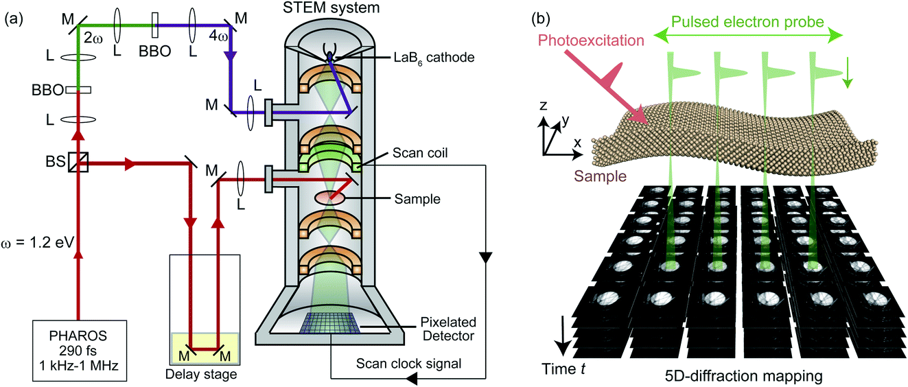 | ||
| Fig. 1 (a) Schematic of the 5D-STEM system. L, M, and BS denote lens, mirror and beam splitter, respectively. Fundamental 1.2 eV light pulse is converted to 4.8 eV by two β-Ba2B2O4 (BBO) crystals and then focused on the LaB6 cathode in the STEM system. The CBED pattern of the photoexcited sample is recorded by the pixelated detector, which is electrically synchronized with the scan coil of STEM. (b) Schematic of the 5D-STEM. The photoexcited sample is probed by scanning the convergent electron pulse in two-dimensional real space (x,y). The time (t)-dependence of two-dimensional (kx,ky) CBED images are obtained at the respective positions. | ||
Fig. 1(b) shows the schematic of strain imaging using the CBED setup in our 5D-STEM system. The sample is excited by the optical pump pulse with 290 fs duration, and strains are induced via a variety of mechanisms, e.g., thermoelasticity.17,18 The pulsed convergent electron beam propagating along the z direction is focused onto a certain position (x,y) of the sample. In this paper, we define the Cartesian coordinates x, y, and z axes based on the propagation direction of the probe electron beam, which is fixed to the laboratory system. There, the two-dimensional (kx,ky) CBED pattern is recorded by the pixelated detector. By scanning the position of the electron beam in the x and y direction, two-dimensional (x, y) mapping of the two-dimensional (kx,ky) CBED patterns can be obtained. Such 4D-STEM data are repeatedly obtained by changing the relative arrival time (t) of the optical pulse (pump) and the electron pulse (probe). This enables us to record the time-evolution of the 4D-STEM data with the time resolution determined by the duration of electron and optical pulses. By analyzing the obtained five-dimensional (x,y,kx,ky,t) dataset, the ultrafast movies of displacement gradient tensor D(x,y,t) can be obtained, as described in Sections 2.3 and 2.4.
We should note that the temporal resolution of the ultrafast electron microscope (and consequently the 5D-STEM) is mainly dominated by the duration of electron pulses, which tend to elongate by the repulsion of electrons within a single pulse, i.e. the space charge effect.19 Therefore, the number of electrons in a single electron pulse must be eliminated to achieve a high enough time resolution. We confirmed that the best temporal resolution of our 5D-STEM system is below 2 ps when we set the number of electrons per pulse to be less than ∼1000.9 In our system, the spatial resolution (15 nm) is restricted by the drift motion of the sample during data acquisition, in contrast to conventional static STEM where it is determined by the spot size of the probe electron beam. This is because the typical 5D-STEM-CBED measurement in our setup requires more than a day for the data acquisition due to the reduced intensity of the photoelectron beam.
2.2 Sample preparation
We use a [001] oriented single-crystalline silicon plate 100 μm × 100 μm × 100 nm as a sample. We deposited a metallic tungsten patterned onto the silicon plate, with ∼100 nm thickness, by the focused-ion beam (FIB) method using NB5000 (Hitachi High-Tech). This metallic tungsten absorbs the pump optical pulse (1.2 eV) while the silicon part shows a very low absorption rate.20 Thus, the patterned tungsten part immediately gets photo-thermalized by the pump and acts as the acoustic phonon generator at the silicon interface. We also fabricated the triangular patterns of voids in the silicon plate by FIB (appearing in Fig. 5). For all of these nanofabrications, we set the acceleration voltage to 40 kV and used the small (15 μm) aperture to avoid damage to the sample.2.3 Calculation of displacement gradient tensor from the CBED pattern
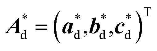
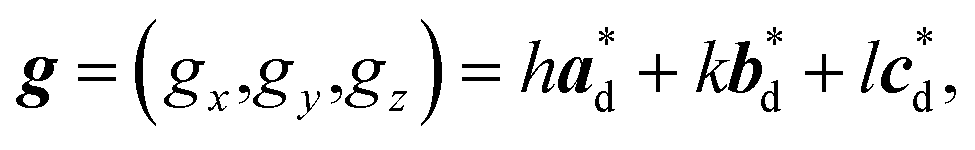
Here, we express the lattice vectors a,b,c and reciprocal lattice vectors a*,b*,c* of the original non-deformed crystal, using matrices A and A* as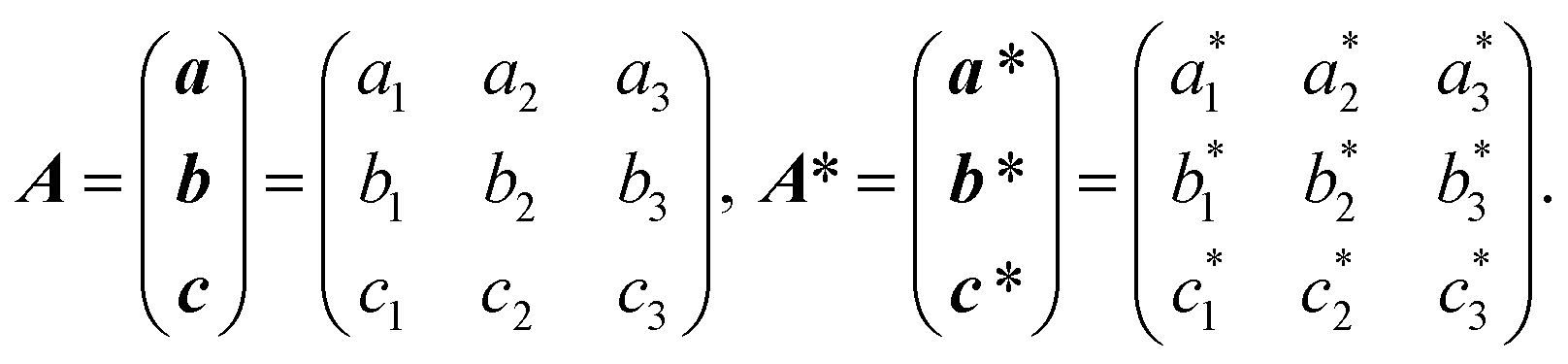
When we assume that R is a rotation matrix that represents the rotation of the crystal with respect to the probe electron beam, and D is the displacement gradient tensor that describes the deformation of the crystal, the lattice parameter of the deformed crystal Ad can be newly expressed as
| Ad = R(E + D)A, |
 can be approximately expressed by
 | (1) |
We use the relations A* = 2π[A−1]T, R−1 = RT, and (E + D)−1 ≃ E − D to derive eqn (1). The superscript T indicates the transpose matrix.
In conventional CBED analysis, the displacement gradient tensor D is calculated from the excess and deficit line positions appearing in the CBED patterns. When the propagation direction of the convergent electron beam is parallel to the z axis, the relations k′ − k = g and k2 = k′2 are satisfied, where 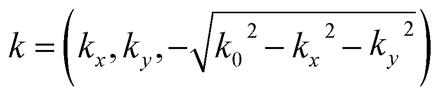 and k′ are the wave vectors of the incident and scattered electron beams, and k0 is the wave number of the incident electron beam. Note that
 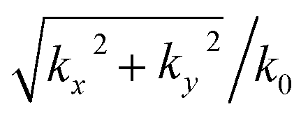 should be smaller than the convergence angle of the probe electron beam. g is the scattering vector that satisfies
 | (2) |
| Deficit line: k·g = −|g|2/2, |
| Excess line: k′·g = |g|2/2, |
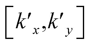 in reciprocal space. In addition, the relations kx,ky ≪ k0 and gz2 ≪ gx2 + gy2 are satisfied considering that the electrons are accelerated to 200 keV. Using these relations, the positions of the deficit and excess lines with respect to the origin of reciprocal space, rd and re, are expressed by
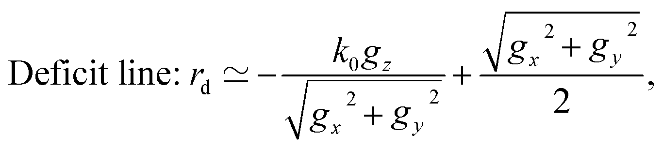 | (3) |
 | (4) |
Using eqn (1)–(4), the displacement gradient tensor D can be calculated from the excess and deficit line positions in the CBED patterns.
In this study, we approximate R ≃ E since the tilting angle of the sample with respect to the electron beam is less than 2° (see Section 3.1). For single-crystalline silicon, A* = 2πE/a holds, where a is the lattice constant of the cubic crystal. When we focus on h00 diffraction in a single-crystalline silicon and ignore the second- and higher-order terms of D, the positions of the deficit and excess lines can be calculated as
 | (5) |
 | (6) |
Therefore, Dxx and Dzx can be calculated form the positions of excess and deficit lines experimentally. Note that all 9 components of D can be determined by measuring the multiple excess and deficit lines at different tilting angles, in principle.21 We determined Dxx, Dyy, Dzx, Dzy as we scanned the beam position and the delay time (x,y,t), by recording the positions of the excess (deficit) lines obtained from the local maxima (minima) of ![[8 with combining macron]](https://www.rsc.org/images/entities/char_0038_0304.gif) 00 and 080 diffraction intensities.
00 and 080 diffraction intensities.
2.4 Derivation of time-dependent strain from 5D-STEM-CBED
Calculation of the photoinduced time-dependent displacement gradient tensor ΔD(x,y,t) = D(x,y,t) − D(x,y,0) from the 5D-STEM data I(x,y,kx,ky,t) can be achieved by simply repeating the CBED analysis for 4D-STEM data, in principle. However, in practice, an additional pre/postprocess is required due to the very low intensity of the probe electron beam. As the number of electrons in a single electron pulse for 5D-STEM is limited to less than <1000 for high time resolution measurements (see Section 2.1), the data acquisition time of more than several weeks is typically required if we simply apply the above analysis for I(x,y,kx,ky,t) at 100 × 100 × 256 × 256 × 100 points. To avoid this problem, we applied an additional process to the 5D-STEM data: (1) 1 × 1 × 3 × 3 × 1 median filter and (2) 5 × 5 × 1 × 1 × 3 average filter are applied to the 5D I(x,y,kx,ky,t) data. Then ΔD is derived by the CBED analysis as described in Section 2.3. Afterwards, (3) 3 × 3 × 1 median filter is applied to the ΔD(x,y,t) data. The two median filters [(1), (3)] are used to remove the impulse noise caused during the measurement and the analysis, respectively. Owing to the average filter (2), the signal-to-noise ratio at a respective point (x,y,t) is improved by ∼100 times. Although the total space- and time-resolutions become slightly worse through these processes, the statistics of the analyzed data greatly improves. These processes are indispensable in practice, since a long acquisition time suppresses the effective space resolution due to the sample drift. It should be noted that owing to these pre/postprocesses, the experimental results appearing in this paper require only about 1 day of data acquisition time. Yet this limits the total space resolution to ∼15 nm, as mentioned above.We parallelized these data processes on a high-performance computer with sufficient memory and calculation cores. This is because the data size of the typical 5D-STEM data (100 × 100 × 256 × 256 × 100 of 32-bit float) is about 300 gigabytes and applying the CBED analysis takes more than a few hours when a single-core system is used for calculation. We employed the shared-memory high-performance computer with 3 terabytes memory and 112 cores for the analysis. For parallelization, we employed Python-based library Dask,22,23 which enables the parallel computation of the above-mentioned processes. Using Dask, the calculation can be easily extended to the much larger data size by utilizing the distributed-memory system, if required.
3 Results and discussion
3.1 Static CBED measurement on 100 nm thick Si plate
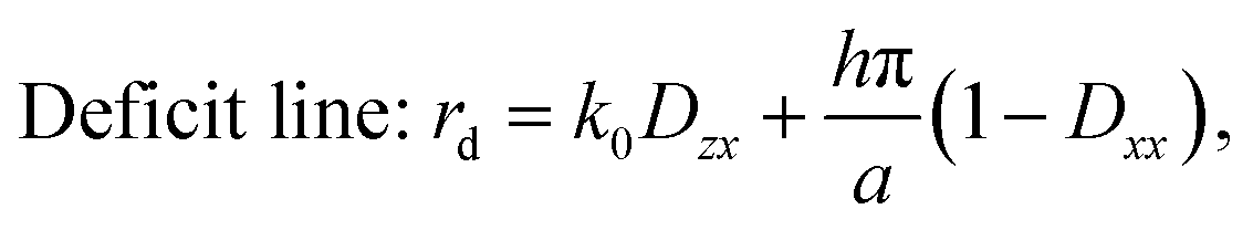
To begin with, we show the result of static CBED measurements on a single-crystalline silicon plate. As shown in Fig. 2(a), we set the [001] oriented silicon plate with [001] parallel to the probe electron beam, and then rotate it by α = 1.9° and β = 0.8° around the x and y axes, respectively. As a result, a, b, and c axes of the single-crystalline silicon are slightly deviated from the x, y, and z axes. The typical CBED pattern under this setup is shown in Fig. 2(b). In the transmitted electron disk, we observe several dark deficit lines, where the electrons are diffracted while travelling through the silicon plate. Correspondingly, the diffracted electrons form the bright excess lines. To determine the Miller indices of these excess and deficit lines, we simulate the CBED pattern of the single crystalline silicon as shown in Fig. 2(c), based on the method described in ref. 16. Most of the observed CBED patterns are reproduced by the simulation, and thus we can assign the Miller indices of the respective lines. Hereafter, we focus on the time dependence of00 and 080 deficit/excess lines to determine the time-dependent displacement gradient tensor ΔD(x,y,t) = D(x,y,t) − D(x,y,0).
 | ||
| Fig. 2 (a) Schematic of the CBED experimental setup. x, y, and z axes are fixed to the laboratory system, and −z corresponds to the propagation direction of the convergent electron beam. The a, b, and c axes of the single-crystalline silicon sample are aligned parallel to x, y, and z axes, and then the sample is rotated by α = 1.9° and β = 0.8° around x and y axes, respectively. (b) Typical CBED pattern for the single-crystalline silicon with a thickness of 100 nm. 00 and 080 excess and deficit lines are indicated by white arrows. (c) Simulated CBED pattern for the single-crystalline silicon sample. | ||
3.2 Strain dynamics in Si plate obtained by 5D-STEM-CBED
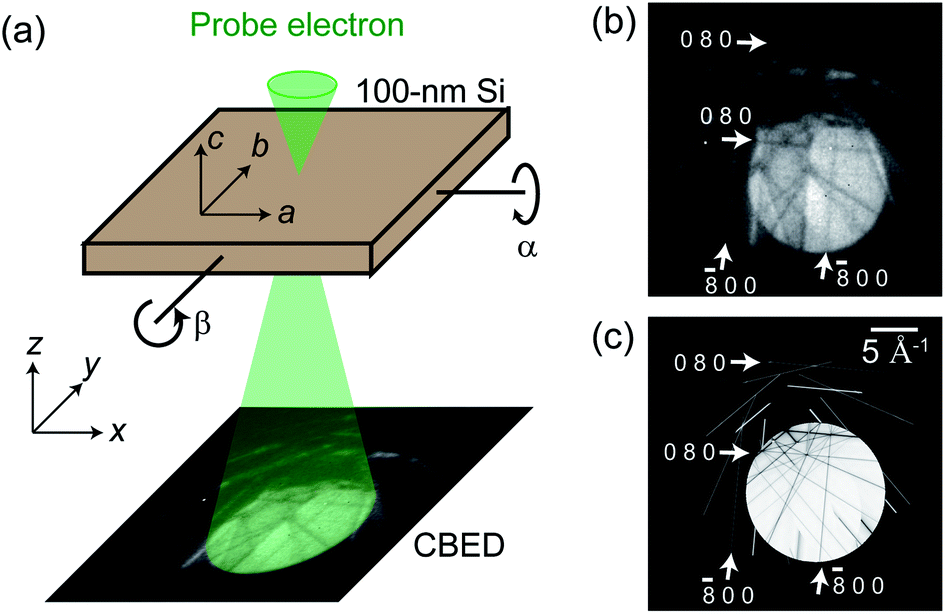
In this section, we demonstrate the quantitative evaluation of the displacement gradient tensor ΔD(x,y,t), derived from the single 5D-STEM data. Here we use the 100 nm-thick silicon plate with a small tungsten nanodisk deposited at the center, which acts as a single point-like source of the photoinduced strain. Fig. 3(a) shows the bright-field image of the sample reconstructed from the 5D-STEM data (t < 0). The metallic tungsten nanodisk (diameter: 700 nm, thickness: 100 nm) is deposited at the center using FIB. The x and y directions are depicted in Fig. 3(a). When the sample is photoexcited by the 1.2 eV pump optical pulse, only the tungsten nanodisk is immediately photo-thermalized because silicon hardly absorbs the 1.2 eV light.20 As a result, the strain is first locally generated around the tungsten nanodisk and starts to propagate in the silicon plate as the radial acoustic waves.18 We quantitatively estimated the amplitude of such acoustic waves by analyzing the t-dependent CBED patterns. The CBED pattern at the position indicated by the green cross is displayed in Fig. 3(b). We analyzed the time dependence of00 excess line [Fig. 3(c)] and estimated ΔD(x,y,t) from the peak position of 00 excess line, following the equations in Section 2.3. We confirmed that the shift of the excess line is identical with the deficit line, which indicates that the observed 00 line shift is mainly caused by ΔDzx, and the contribution from ΔDxx is invisibly small in the present setup. Resulting time dependent imaging of ΔDzx(x,y,t) is shown in Fig. 3(d). The generation and radial propagation of the strain is clearly visualized quantitatively. In the same way, we estimated ΔDzy(x,y,t) from the 080 excess line position as shown in Fig. 3(e). As the (100) and (010) planes are crystallographically equivalent, the amplitude of ΔDzx(x,y,t) is almost identical with ΔDzy(x,y,t) when the image is rotated by 90°. These measurements can determine the amplitude and polarization of the propagating acoustic waves experimentally, which had been technically difficult in the conventional time-dependent bright-field image and diffractions.5,9
 | ||
| Fig. 3 (a) The bright-field image of silicon single crystal on which a tungsten nanodisk (700 nm diameter) is deposited. (b) CBED pattern at the position depicted by the green cross in (a). (c) Time dependence of 00 excess line. The position of 00 excess line is shifted after photoexcitation. (d, and e) Time dependence of displacement gradient tensor component ΔDzx(x,y,t) and ΔDzy(x,y,t) calculated from the 5D-STEM data. The scale bars indicate 2 μm. The black circle at the center indicates the tungsten nanodisk. | ||
Fourier-transformation analysis on ΔDzx(x,y,t) and ΔDzy(x,y,t) reveals the distribution of strains in the momentum–frequency (κ–ω) space. Fig. 4(a) shows the time dependence of ΔDzx(x,y,t) recorded along the red arrow in Fig. 3(a). The wavelength of the strain wave seemingly changes as a function of position and t, indicating that the oscillatory behavior is composed of multiple modes with different sound velocities. We applied the x, y, t Fourier transformation to ΔDzx(x,y,t) and obtained Δ![[D with combining tilde]](https://www.rsc.org/images/entities/i_char_0044_0303.gif) zx(κx,κy,ω), which shows the strain distribution in κ–ω space. In Fig. 4(b), we show Δzx corresponding to the Fourier transformation of Fig. 4(a). The red curves show the theoretical acoustic eigen modes in a 100 nm thick silicon plate, calculated using the partial wave technique.24 In this frequency region, there are two dispersion curves corresponding to the so-called symmetric (S0) and asymmetric (A0) modes, which describe the plate-wave mode with symmetric and asymmetric strain distributions along the thickness direction, respectively. The obtained strain distribution in the κ–ω space suggests that the asymmetric A0 mode is mainly excited in the frequency region of ω < 0.5 GHz. Since the tungsten is deposited only on the top side of the plate sample, the asymmetric A0 mode is more likely to be excited by the photo-thermalization of the tungsten disk. In addition, we further obtained the constant frequency cut of
zx(κx,κy,ω), which shows the strain distribution in κ–ω space. In Fig. 4(b), we show Δzx corresponding to the Fourier transformation of Fig. 4(a). The red curves show the theoretical acoustic eigen modes in a 100 nm thick silicon plate, calculated using the partial wave technique.24 In this frequency region, there are two dispersion curves corresponding to the so-called symmetric (S0) and asymmetric (A0) modes, which describe the plate-wave mode with symmetric and asymmetric strain distributions along the thickness direction, respectively. The obtained strain distribution in the κ–ω space suggests that the asymmetric A0 mode is mainly excited in the frequency region of ω < 0.5 GHz. Since the tungsten is deposited only on the top side of the plate sample, the asymmetric A0 mode is more likely to be excited by the photo-thermalization of the tungsten disk. In addition, we further obtained the constant frequency cut of  , which successfully visualizes the in-plane anisotropy of the sound (A0 mode) velocity. To remove the contribution from the static structure at ω = 0, we show
 ![[S with combining tilde]](https://www.rsc.org/images/entities/i_char_0053_0303.gif) (κx,κy,ω)/((κx,κy,0) in Fig. 4(c–e). Moreover, we applied four-fold symmetrization based on the crystallographic symmetry of the silicon single crystal. Although the constant frequency cut shows the almost isotropic circular feature of the A0 mode dispersion relation, slight 4-fold anisotropy appears at 1.43 GHz. This may be caused by the crystallographic anisotropy of the cubic silicon single crystal.
(κx,κy,ω)/((κx,κy,0) in Fig. 4(c–e). Moreover, we applied four-fold symmetrization based on the crystallographic symmetry of the silicon single crystal. Although the constant frequency cut shows the almost isotropic circular feature of the A0 mode dispersion relation, slight 4-fold anisotropy appears at 1.43 GHz. This may be caused by the crystallographic anisotropy of the cubic silicon single crystal.
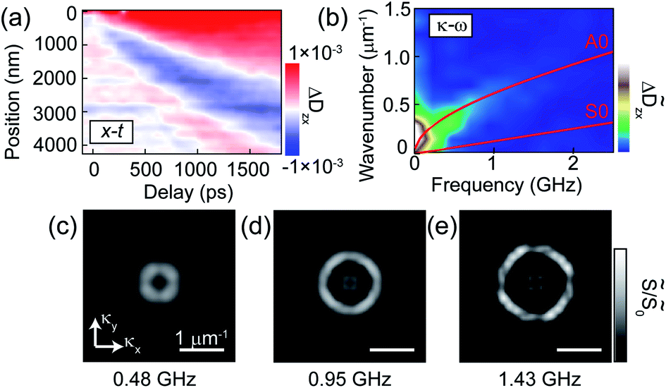 | ||
| Fig. 4 (a) Space-time dependence of ΔDzx along the red arrow in Fig. 3(a). (b) Fourier transformation of the ΔDzx in (a). Red curves indicate the theoretical acoustic dispersion relation of zeroth-order asymmetric (A0) and symmetric (S0) modes in the 100 nm silicon thin plate. (c–e) /0 = (κx,κy,ω)/((κx,κy,0) at 0.48, 0.95, and 1.43 GHz, respectively. | ||
3.3 Pros and cons of the 5D-STEM-CBED method
The data in Fig. 3 and 4 demonstrate that the quantitative estimation of strains with nm × ps resolution can be achieved by analyzing 5D-STEM-CBED. We can also extract the strain distribution in κ–ω space, from which the in-plane anisotropy of the sound velocities and acoustic dispersion curves can be obtained. We emphasize that all images in Fig. 3 and 4 are obtained by analyzing a single 5D-STEM piece of data with 5 axes (x,y,kx,ky,t). Once the single 5D-STEM data is obtained, the displacement gradient tensor D(x,y,t) at arbitrary position and time can be evaluated by postprocessing. As compared to ref. 16 where ultrafast CBED-STEM analysis has been done along a single axis in real space, our 5D-STEM system is capable of taking a full two-dimensional ultrafast movie of the strain. As a result, propagation of strain along the arbitrary direction can be evaluated at the same time as demonstrated in Fig. 3(d, e) and 4(c–e). We also note that the quantitative estimation of the displacement gradient tensor can be applied to all types of single crystals. Such a method should play an important role in exploring the unique ultrafast strain dynamics in future acoustic nano-devices.On the other hand, 5D-STEM-CBED suffers from long data acquisition time as compared to the usual ultrafast bright-field imaging method, where the spatial resolution also tends to get worse due to the sample drift. Although increasing the repetition rate of the laser should partly solve this problem, there is a clear limit because of sample damage becoming serious at higher repetition rates. Therefore, practically, compensating such low S/N ratio by data processing is one of the key techniques in 5D-STEM. As described in Section 2.4, we applied several median and average filters along the x, y, and t axes which significantly improve the data quality. Increasing the number of electrons per pulse without spreading the pulse duration may be necessary to achieve ∼1 nm space resolution in future. Such improvement of a future 5D-STEM system may become possible by utilizing pulse compression techniques.25,26
3.4 Practical application of 5D-STEM-CBED on nano-patterned Si plate
Finally, we show a practical demonstration of 5D-STEM-CBED for nanofabricated samples. We prepared two types of samples as shown in Fig. 5(a and b). Similar to Fig. 3(a), the metallic tungsten is deposited in a bar shape (400 nm width, 100 nm thickness) at the left side of each sample. They work as the line-like source of the photoinduced strain waves. Moreover, we fabricated the array of the 700 nm triangular voids at the center, the direction of which in Sample #1 is opposite to Sample #2. As previously reported,27,28 scattering of the acoustic waves is strongly affected by the direction of the triangles in such samples. We quantitatively evaluated the t-dependent displacement gradient tensor ΔD(x,y,t) in these samples. In Sample #1, the acoustic strain waves are emitted from the metallic tungsten bar at the left edge and start to propagate horizontally [Fig. 5(c1–c3)]. As the acoustic wave passes through the array of triangular voids, the amplitude is seemingly not strongly affected [Fig. 5(c4–c6)]. This is also confirmed by the space–time dependence of ΔDzxav(x,t) in Fig. 5(e), which is obtained by averaging ΔDxz(x,y,t) along the vertical (y) direction. In Sample #2, we also observed similar emission of the acoustic wave from the tungsten bar in the t = 0–2 ns region [Fig. 5(d1–d3)]. However, as the strain wave propagate through the triangular voids, the amplitude apparently becomes suppressed [Fig. 5(d4–d6)]. To quantitatively compare the amplitudes of strain waves in Samples #1 and #2, we show ΔDzxav at t = 800 ps in Fig. 5(g). ΔDzx in Samples #1 and #2 are comparable in this t-range, indicating that the photogeneration of strains similarly occurs for both samples. In contrast, the amplitude of the acoustic wave in Sample #2 at 4200 ps [Fig. 5(h)] is significantly suppressed as compared to that of Sample #1. These results suggest that the scattering process of the acoustic strain is quantitatively different in such directionally nano-patterned artificial systems.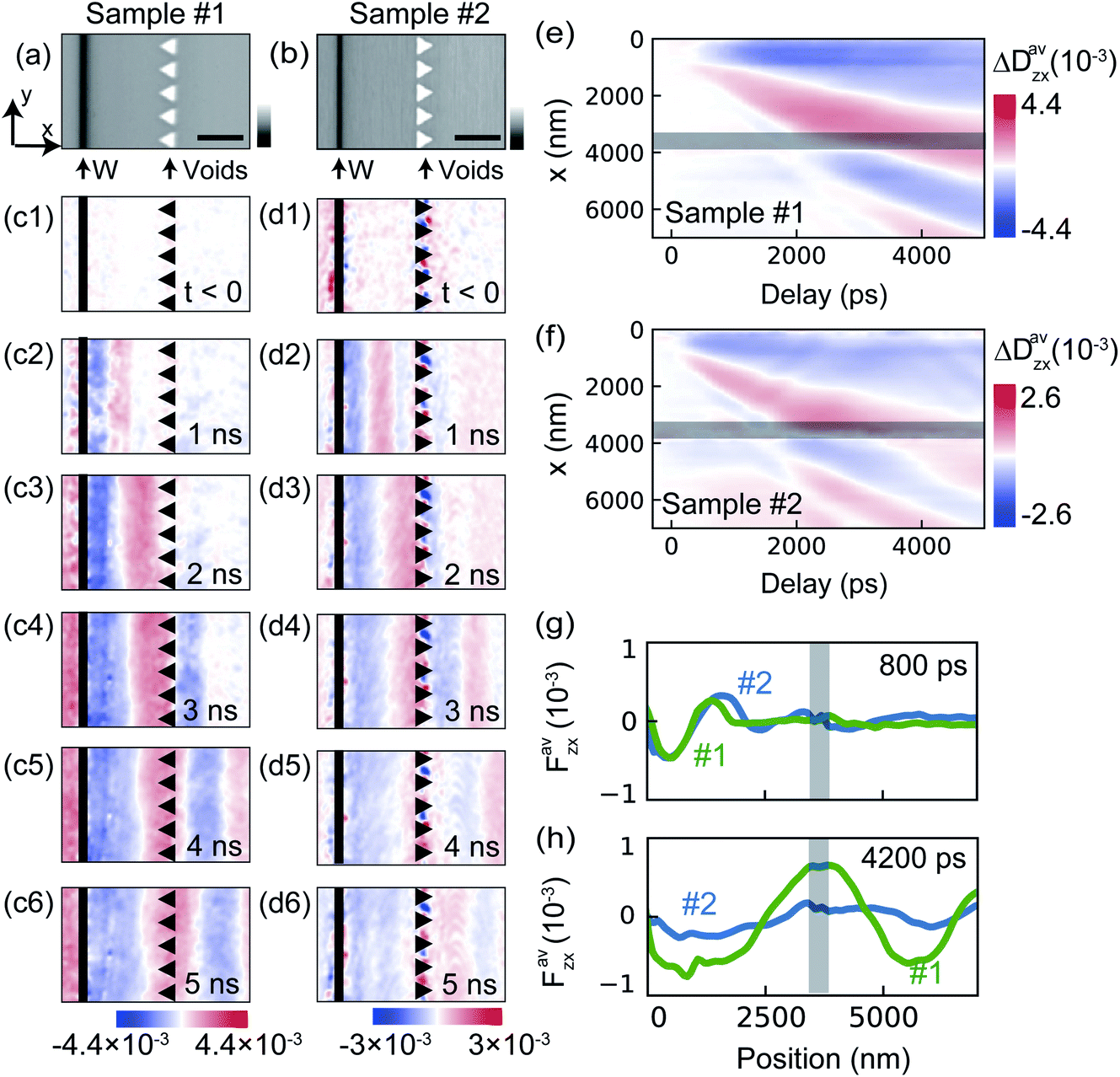 | ||
| Fig. 5 (a and b) Bright-field images of Samples #1 and #2. The scale bar denotes 2 μm. The black region corresponds to the deposited tungsten bar. The white triangles are voids fabricated by FIB. (c and d) Time dependence of ΔDzx(x,y,t) calculated by the 5D-STEM-CBED analysis. The black line and triangles indicate the deposited tungsten bars and the triangular voids, respectively. (e and f) Position and time dependence of ΔDzxav(x,t) for Samples #1 and #2, obtained by averaging ΔDzx(x,y,t) along the y direction. (g and h) ΔDzxav(x,t) at 800 and 4200 ps, respectively. The gray shaded regions in (e–j) denote the position where the triangular void patterns are fabricated. | ||
4 Conclusions
We have demonstrated 5D-STEM-CBED analysis for the quantitative time-dependent mapping of optically-induced strains. 5D-STEM measurement on 100 nm silicon single crystal with the metallic tungsten patterns deposited as the acoustic wave source demonstrated that time-dependent strain and polarization can be quantitatively mapped in two-dimensional space from the CBED analysis. By Fourier-transformation analysis, we further characterized the distribution of strains in the momentum-frequency space, which can be used to reveal anisotropic sound velocities and dispersion curves along an arbitrary direction within the plate. We emphasize that the analysis of 5D-STEM requires additional pre/postprocesses to compensate the low S/N ratio. The data size of 5D-STEM is more than a few hundreds of gigabytes, and thus the analysis requires efficient parallel computing. Nonetheless, the quantitative evaluation of strains by 5D-STEM-CBED enabled us to visualize the directional properties of acoustic waves realized in the Si plate that was artificially patterned with arrays of triangular voids. Such a 5D-STEM method will play a versatile and important role in the future development of optically controlled nanometer-scale acoustic phenomena and functions.Conflicts of interest
There are no conflicts of interest to declare.Acknowledgements
This work was partially supported by grant-in-aid for Scientific Research (KAKENHI) (Grant No. 21K14488), MEXT Quantum Leap Flagship Program (MEXT Q-LEAP).References
- A. H. Zewail, Annu. Rev. Phys. Chem., 2006, 57, 65 CrossRef CAS PubMed.
- A. Adhikari, J. K. Eliason, J. Sun, R. Bose, D. J. Flannigan and O. F. Mohammed, ACS Appl. Mater. Interfaces, 2017, 9, 3 CrossRef CAS PubMed.
- P. Baum, D.-S. Yang and A. H. Zewail, Science, 2007, 318, 788 CrossRef CAS PubMed.
- M. Eichberger, H. Schäfer, M. Krumova, M. Beyer, J. Demsar, H. Berger, G. Moriena, G. Sciaini and R. J. D. Miller, Nature, 2010, 468, 799 CrossRef CAS PubMed.
- D. R. Cremons, D. A. Plemmons and D. J. Flannigan, Nat. Commun., 2016, 7, 11230 CrossRef CAS PubMed.
- X. Fu, F. Barantani, S. Gargiulo, I. Madan, G. Berruto, T. LaGrange, L. Jin, J. Wu, G. M. Vanacore, F. Carbone and Y. Zhu, Nat. Commun., 2020, 11, 5770 CrossRef CAS PubMed.
- G. Berruto, I. Madan, Y. Murooka, G. M. Vanacore, E. Pomarico, J. Rajeswari, R. Lamb, P. Huang, A. J. Kruchkov, Y. Togawa, T. Lagrange, D. Mcgrouther, H. M. Rønnow and F. Carbone, Phys. Rev. Lett., 2018, 120, 117201 CrossRef CAS PubMed.
- T. Shimojima, A. Nakamura, X. Yu, K. Karube, Y. Taguchi, Y. Tokura and K. Ishizaka, Sci. Adv., 2021, 7, 1322 CrossRef PubMed.
- A. Nakamura, T. Shimojima, Y. Chiashi, M. Kamitani, H. Sakai, S. Ishiwata, H. Li and K. Ishizaka, Nano Lett., 2020, 20, 4932 CrossRef CAS PubMed.
- M. Harb, W. Peng, G. Sciaini, C. T. Hebeisen, R. Ernstorfer, M. A. Eriksson, M. G. Lagally, S. G. Kruglik and R. J. D. Miller, Phys. Rev. B: Condens. Matter Mater. Phys., 2009, 79, 94301 CrossRef.
- D. R. Cremons, D. A. Plemmons and D. J. Flannigan, Struct. Dyn., 2017, 4, 44019 CrossRef PubMed.
- K. Maaz, The Transmission Electron Microscope - Theory and Applications, InTech, 2015 Search PubMed.
- D. X. Du and D. J. Flannigan, Struct. Dyn., 2020, 7, 24103 CrossRef CAS PubMed.
- C. Ophus, Microsc. Microanal., 2019, 25, 563 CrossRef CAS PubMed.
- T. Shimojima, A. Nakamura, and K. Ishizaka, in preparation.
- A. Feist, N. Rubiano da Silva, W. Liang, C. Ropers and S. Schäfer, Struct. Dyn., 2018, 5, 14302 CrossRef PubMed.
- C. Thomsen, H. T. Grahn, H. J. Maris and J. Tauc, Phys. Rev. B: Condens. Matter Mater. Phys., 1986, 34, 4129 CrossRef CAS PubMed.
- P. Ruello and V. E. Gusev, Ultrasonics, 2015, 56, 21 CrossRef CAS PubMed.
- B. J. Siwick, J. R. Dwyer, R. E. Jordan and R. J. D. Miller, Chem. Phys., 2004, 299, 285 CrossRef CAS.
- C. Schinke, P. Christian Peest, J. Schmidt, R. Brendel, K. Bothe, M. R. Vogt, I. Kröger, S. Winter, A. Schirmacher, S. Lim, H. T. Nguyen and D. Macdonald, AIP Adv., 2015, 5, 67168 CrossRef.
- Y. Martin, J. L. Rouviere, J. M. Zuo and V. Favre-Nicolin, Ultramicroscopy, 2016, 160, 64 CrossRef CAS PubMed.
- M. Rocklin, PROC. 14th PYTHON Sci. CONF, 2015.
- C. R. Harris, K. Jarrod Millman, S. J. van der Walt, R. Gommers, P. Virtanen, D. Cournapeau, E. Wieser, J. Taylor, S. Berg, N. J. Smith, R. Kern, M. Picus, S. Hoyer, M. H. van Kerkwijk, M. Brett, A. Haldane, J. Fernández del Río, M. Wiebe, P. Peterson, P. Gérard-Marchant, K. Sheppard, T. Reddy, W. Weckesser, H. Abbasi, C. Gohlke and T. E. Oliphant, Nature, 2020, 585, 357 CrossRef CAS PubMed.
- J. Rose, Ultrasonic Waves in Solid Media, Cambridge University Press, Cambridge, 1999 Search PubMed.
- T. Van Oudheusden, E. F. De Jong, S. B. Van Der Geer, W. P. E. M. Op T Root, O. J. Luiten and B. J. Siwick, J. Appl. Phys., 2007, 102, 93501 CrossRef.
- R. P. Chatelain, V. R. Morrison, C. Godbout and B. J. Siwick, Appl. Phys. Lett., 2012, 101, 81901 CrossRef.
- S. Shirota, R. Krishnan, Y. Tanaka and N. Nishiguchi, Jpn. J. Appl. Phys., 2007, 46, L1025 CrossRef CAS.
- S. Danworaphong, T. A. Kelf, O. Matsuda, M. Tomoda, Y. Tanaka, N. Nishiguchi, O. B. Wright, Y. Nishijima, K. Ueno, S. Juodkazis and H. Misawa, Appl. Phys. Lett., 2011, 99, 201910 CrossRef.
| This journal is © The Royal Society of Chemistry 2022 |