 Open Access Article
 This Open Access Article is licensed under a
 Creative Commons Attribution 3.0 Unported Licence
Characterization of buried interfaces using Ga Kα hard X-ray photoelectron spectroscopy (HAXPES)†
B. F.
Spencer
 *a,
S. A.
Church
b,
P.
Thompson
c,
D. J. H.
Cant
d,
S.
Maniyarasu
b,
A.
Theodosiou
e,
A. N.
Jones
e,
M. J.
Kappers
f,
D. J.
Binks
b,
R. A.
Oliver
f,
J.
Higgins
g,
A. G.
Thomas
a,
T.
Thomson
c,
A. G.
Shard
d and
W. R.
Flavell
*b
*a,
S. A.
Church
b,
P.
Thompson
c,
D. J. H.
Cant
d,
S.
Maniyarasu
b,
A.
Theodosiou
e,
A. N.
Jones
e,
M. J.
Kappers
f,
D. J.
Binks
b,
R. A.
Oliver
f,
J.
Higgins
g,
A. G.
Thomas
a,
T.
Thomson
c,
A. G.
Shard
d and
W. R.
Flavell
*b
aHenry Royce Institute, Photon Science Institute, Department of Materials, School of Natural Sciences, The University of Manchester, Manchester, M13 9PL, UK. E-mail: ben.spencer@manchester.ac.uk
bHenry Royce Institute, Photon Science Institute, Department of Physics and Astronomy, School of Natural Sciences, The University of Manchester, Manchester, M13 9PL, UK. E-mail: wendy.flavell@manchester.ac.uk
cDepartment of Computer Science, School of Engineering, The University of Manchester, Manchester, M13 9PL, UK
dSurface Technologies, Chemical and Biological Sciences Department, National Physical Laboratory, Hampton Road, Teddington, TW11 0LW, UK
eThe Nuclear Graphite Research Group, The University of Manchester, Oxford Road, Manchester, M13 9PL, UK
fDepartment of Materials Science & Metallurgy, University of Cambridge, 27 Charles Babbage Road, Cambridge, CB3 0FS, UK
gRolls Royce PLC, London, UK
First published on 9th May 2022
Abstract
The extension of X-ray photoelectron spectroscopy (XPS) to measure layers and interfaces below the uppermost surface requires higher X-ray energies and electron energy analysers capable of measuring higher electron kinetic energies. This has been enabled at synchrotron radiation facilities and by using lab-based instruments which are now available with sufficient sensitivity for measurements to be performed on reasonable timescales. Here, we detail measurements on buried interfaces using a Ga Kα (9.25 keV) metal jet X-ray source and an EW4000 energy analyser (ScientaOmicron GmbH) in the Henry Royce Institute at the University of Manchester. Development of the technique has required the calculation of relative sensitivity factors (RSFs) to enable quantification analogous to Al Kα XPS, and here we provide further substantiation of the Ga Kα RSF library. Examples of buried interfaces include layers of memory and energy materials below top electrode layers, semiconductor heterostructures, ions implanted in graphite, oxide layers at metallic surfaces, and core–shell nanoparticles. The use of an angle-resolved mode enables depth profiling from the surface into the bulk, and is complemented with surface-sensitive XPS. Inelastic background modelling allows the extraction of information about buried layers at depths up to 20 times the photoelectron inelastic mean free path.
1. Introduction
Hard X-ray photoelectron spectroscopy (HAXPES) extends the sampling depth of X-ray photoelectron spectroscopy (XPS) below the topmost surface for the detection of bulk-like materials and buried interfaces by increasing photoelectron kinetic energies and, thus, escape depths.1 The recent development of laboratory-based HAXPES instruments is expected to lead to an accelerated uptake of this technique by a broad range of researchers; currently, commercial systems using monochromated Ag Lα (2.98 keV), Cr Kα (5.41 keV), and Ga Kα (9.25 keV) are available, with X-ray energies higher than those of traditional lab-based XPS systems, which typically use monochromated Al Kα X-ray sources (1.49 keV).2 Here, we demonstrate measurements made using a Ga Kα HAXPES instrument, with the highest photon energy currently available from a commercial lab-based photoelectron spectrometer, manufactured by ScientaOmicron GmbH3 in the Henry Royce Institute at the University of Manchester. These measurements include the detection of layers buried below 200 nm of organic material using inelastic background modelling,4 where an angle-resolved mode of the EW4000 analyser was also used to obtain depth profiles from the maximum sampling depth towards the surface. Relative sensitivity factors (RSFs) were developed, including the important recent calculations of non-dipole contributions by Trzhaskovskaya and Yarzhemsky,5,6 and these were verified using standard materials.4 More recently, the instrument was used to depth profile through mixed-cation perovskite materials, where these RSFs were again utilised and, notably, HAXPES provided a greater sensitivity to the dilute elements Cs and Rb than can be achieved using XPS.7 We have also combined HAXPES with other destructive depth-profiling techniques, where it was found that HAXPES is able to sample below the damage layer created by plasma etching in glow discharge optical emission spectroscopy (GDOES), a technique which has traditionally been challenging to calibrate.8 This demonstrates that HAXPES is sensitive to the material below the altered layer on an ion-etched surface, and therefore offers measurement of the unmodified chemical composition prior to ion-induced damage and preferential sputtering. As all forms of etching (using monoatomic and more recent cluster sources) potentially alter material systems,9 an important benefit of HAXPES analysis is to provide a minimally-destructive measurement of the material below the topmost surface.Work to date has demonstrated that, by using primary photoelectron peaks in the elastic limit (where photoelectrons leave the sample for detection without loss of energy), Ga Kα HAXPES can increase the sampling depth, defined as three times the effective electron attenuation length, from a maximum of ∼10 nm (measuring C 1s in graphite using Al Kα X-rays, where the inelastic mean free path of electrons is calculated using the well-established TPP-2M formula) to ∼51 nm, approximating the effective attenuation length as the inelastic mean free path of electrons.10 Use of the inelastic background has been demonstrated to further increase this depth-profiling capability, in enabling information to be extracted from a greater inelastic sampling depth (even when primary photoelectron peaks are no longer detected) of up to twenty times the effective electron attenuation length (potentially corresponding to more than hundreds of nm).4
In this paper, we describe the measurement of buried interfaces using core-level photoelectron peaks, angle-resolved measurements, and inelastic background analysis, through five case studies: InxGa1−xN/GaN heterostructures, probing MnxAl1−x below a top capping layer, measuring below the surface oxide passivation layer in zirconium, Cs+ ions implanted in graphite, and measuring through thicker shelled polymer core/shell nanoparticles. These case studies together demonstrate the potential for characterizing buried interfaces using laboratory-based HAXPES.
2. Experimental
The ScientaOmicron HAXPES spectrometer has been detailed previously, and the instrument at the Royce Institute is shown in Fig. 1.4,11 In brief, the instrument is comprised of a Ga metal jet X-ray source (Excillum),12 a bespoke monochromator, and an EW4000 electron energy analyser capable of measuring photoelectrons with kinetic energies up to 12 keV. The liquid metal jet provides a constantly refreshed anode material, enabling the use of a 70 kV electron gun at 250 W. The monochromator removes additional emission lines to isolate Ga Kα1 X-rays (9.2517 keV photon energy),13 as well as focussing the X-ray beam to ca. 50 × 50 μm at the sample position. This yields a relatively high X-ray flux in the laboratory environment, ca. three orders of magnitude greater than traditional lab sources for XPS, such as monochromated Al Kα sources (1.486 keV photon energy).11 This, crucially, enables HAXPES measurements to be undertaken on reasonable timescales, analogous to spectrometers for XPS, overcoming sensitivity issues. The relative sensitivity to some photoelectron peaks (particularly for light elements) is heavily influenced by the photoionization cross section,4 which in some cases drops by up to three orders of magnitude as the photon energy is increased from 1.5 to 9 keV.6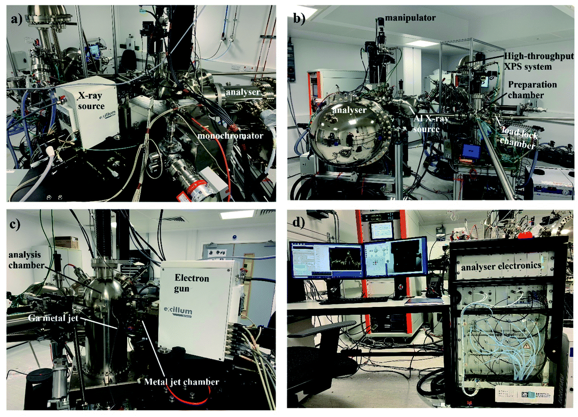 | ||
| Fig. 1 Photographs of the HAXPES system (ScientaOmicron GmbH) at the Henry Royce Institute, (a) the X-ray source and monochromator, (b) the analyser, preparation chamber and separate XPS system (linked via ultra-high vacuum transfer lines), (c) the metal jet capillary and X-ray generation chamber, and (d) the analyser and instrument electronics racks. | ||
The metal jet, monochromator, and analysis chamber are isolated vacuum chambers; the base pressure in the analysis chamber is 1 × 10⁻¹⁰ mbar. Insulated material may be measured using an electron flood source (PREVAC) to replenish electrons at the surface, and differential charging may be avoided by floating the sample (detaching the sample manipulator from the ground). An Al Kα X-ray source is also mounted on the analysis chamber for the comparison of HAXPES with traditional surface-sensitive XPS. The HAXPES instrument is connected via ultra-high-vacuum transfer lines to a high-throughput ESCA2SR spectrometer with monoatomic Ar+ ion etching (10 mA, 2–5 kV, FOCUS GmbH) and a cluster-ion-etching source (GCIB-10S, Ionopktica), as well as an ultra-violet source for UPS measurements (typically generating He II photons at 40.81 eV energy),14 and a preparation chamber with a variety of ports available for additional instrumentation.
The EW4000 analyser may be operated in transmission mode or using angle-resolved modes, AR45 (with a total angular range of 45°), AR56 (total angular range of 56°), or AR60 (total angular range of 60°). The analyser entrance slit has a large acceptable angle of 60°, and the angular modes are used to transmit photoelectrons emitted at each angle directly to the 2D detector after they pass through the entrance slit, whereby the y-axis on the charge-coupled device detector image becomes the photoemission angle (which may then be converted to sampling depth).4 This enables angle-resolved information to be captured in one shot as the sample is held in one position. The sampling depth, ds, is defined as three times the electron effective attenuation length, which in the case of negligible elastic scattering is equivalent to three times the electron inelastic mean free path (IMFP, λi), and is reduced with increasing the photoemission angle, ϑ, with respect to the surface normal, according to4
dS = 3λi![[thin space (1/6-em)]](https://www.rsc.org/images/entities/char_2009.gif) cosϑ, cosϑ, | (1) |
The angle-resolved mode may therefore be particularly useful for samples with lateral microstructure (such as patterning), or if homogeneity is a concern, as it avoids small changes in sample position which might occur as the sample tilt is adjusted. A sputter-cleaned polycrystalline gold reference sample was measured using the angle-resolved mode in order to characterise both the relative detector response and the natural decline in the photoelectron intensity with increasing photoemission angle (extracted via peak fitting the Au 3d5/2 peak at each angle in the 2D angle-resolved data with a simple Gaussian), so that normalized angular profiles of photoelectron intensity (again extracted via peak fitting a photoelectron peak) may be generated by dividing the measured angle-resolved photoelectron intensity by the Au 3d5/2 reference function. Angle-resolved measurements, however, may be limited by the roughness of the sample, as well as the amount of elastic scattering.4
Energy resolution down to approximately 0.5 eV is achievable, as measured using the Fermi edge on a gold reference sample,3 and the resolution and count rate may be adjusted with a combination of entrance slit width adjustment and the choice of analyser pass energy.3 For the data presented here, survey spectra were measured using a 1.5 mm slit width and 500 eV pass energy. High resolution spectra were acquired with a 1.5 mm slit width and 100 eV pass energy, a 0.8 mm slit with 200 eV pass energy, or a 0.3 mm slit width and 500 eV pass energy (which all achieve a similar resolution with differing count rates). In transmission mode, the complete binding energy (BE) range is measurable (that is, up to kinetic energies ∼9.25 keV) at all pass energies, however, for the angle-resolved modes, the upper kinetic energy range is limited by the pass energy; for the complete BE range to be measured, 500 eV pass energy is required.
3. Results and discussion
3.1. InGaN/GaN heterostructures
InxGa1−xN/GaN quantum well (QW) heterostructures are important material systems for light emitting diodes.15 Their optical properties are influenced by competing radiative and non-radiative recombination mechanisms; these are affected by strong internal electric fields in these structures (up to MV cm−1).16 The optical properties of these heterostructures may be altered by engineering the material structure, such as variations in the In content of the InxGa1−xN QWs, the width of the QWs, the width of the GaN capping layer, and the inclusion of a doped underlayer.17 Indeed, research into this material system continues because the internal quantum efficiency drops significantly with increasing emission wavelength (the ‘green gap’),17 a process which has been attributed to intrinsic field effects, alloy fluctuations and nonradiative defects.18,19The internal electric fields lead to shifts in the electronic bands (band bending) at the interfaces, because the Fermi level is pinned at the surface, and therefore a measurement of band bending in a depth-resolving fashion would provide useful insights into the electronic structure within the stack, which is a crucial factor in determining device performance. XPS has been used to measure changes in the band bending at the surface with laser photoexcitation, by measuring changes in the binding energy of elemental core levels after carrier creation with time-resolution and chemical specificity.20–23 Gaining depth resolution in such measurements for depletion region widths in excess of typical XPS sampling depths requires an extension of the sampling depth enabled by HAXPES, as demonstrated on GaN by Ueda using 5.95 keV X-rays at the BL15XU end station at SPring-8.24 Similarly, Narita et al. measured changes in the band bending at the GaN surface after etching-induced damage, using 7.94 keV X-rays at the BL46XU end station.25 In both studies, the photoemission angle, ϑ, was varied to reduce the sampling depth by cosϑ, according to eqn (1).
Here, we demonstrate HAXPES measurements using the 9.25 keV laboratory source, on a set of InxGa1−xN/GaN heterostructures (a QW typically 3 nm thick, with varying In content, on top of 2.5 μm GaN, with a 7.5 nm GaN capping layer) on (0001) sapphire substrates, prepared by metal–organic chemical vapor deposition and characterised using high-resolution transmission electron microscopy and electron energy loss spectroscopy.26,27Fig. 2 shows normal emission HAXPES (Fig. 2(a)) and Al Kα XPS survey spectra (Fig. 2(b)) for a typical QW structure, as illustrated in Fig. 2(c), containing 19% In (In0.19Ga0.81N) with a 3.2 nm thick QW. XPS measurements were taken at normal emission, and HAXPES using grazing incidence with a photoemission angle of 4° in transmission mode (Fig. 2(d)). For Al Kα XPS, there is an unfortunate overlap of the N 1s and Ga LMM signals, which is removed at different photon energies and has also recently been demonstrated using a Cr Kα laboratory HAXPES system.28 No peaks associated with In are observed using XPS, which is dominated by surface contamination containing carbon and oxygen, whereas In 3s, p, d are observed with HAXPES, along with the deeper core levels In 2s and 2p.
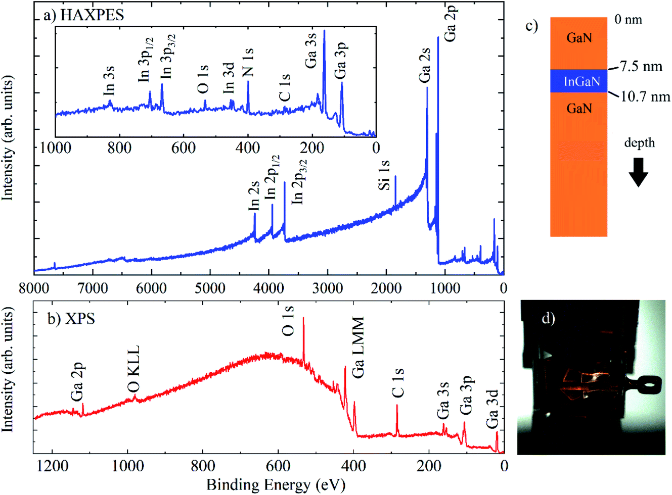 | ||
| Fig. 2 (a) HAXPES (with the low BE region shown in the inset) and (b) Al Kα XPS survey spectra for an InGaN/GaN heterostructure (In0.19Ga0.81N, 3.2 nm thick), as shown in the schematic in (c). (d) Photograph of samples on sample plate on the manipulator. | ||
HAXPES was performed on a set of QWs with nominal InxGa(1−x)N compositions of x = 0.05, 0.15, 0.19, and 0.25, with QW widths of 2.8 nm, 2.9 nm, 3.2 nm and 3.3 nm, respectively, all with 7.5 nm GaN capping layers. Because the samples were prepared on insulating sapphire substrates, the electron flood source charge neutraliser was required to remove charging under the X-rays. Energy referencing of the HAXPES spectra was performed using the Ga 2p3/2 peak at 1117.8 eV, expected for GaN, and measured with XPS after energy referencing using C 1s at 284.8 eV. This gave BE positions for In 3d5/2 at ∼444 eV and N 1s at ∼397 eV, also as expected.29 The use of C 1s for charge referencing in HAXPES (when it is measurable) is not recommended due to non-negligible recoil effects for light atoms at high photoelectron kinetic energies.30
Calculations of atomic concentrations were performed using established relative sensitivity factors (RSFs) for the Ga Kα instrument,4 which have now been refined and expanded by Cant et al. into an important new tool which allows researchers to calculate RSFs for all atomic core levels measured with X-ray photon energies in the range 1.5–10 keV and in any instrument geometry.31 Calculations were carried out using both the In 2p3/2 core level and the In 3d core level, as shown in Table 1, using high resolution core level spectra obtained at grazing incidence in transmission mode. Errors were estimated using relative changes in at% calculated using a range of acceptable background fits (as judged by eye), as well as the associated RSF.
| Nominal x for InxGa(1−x)N | Measured using In 2p | Measured using In 3d | |||||
|---|---|---|---|---|---|---|---|
| Ga at%, ±0.3 at% | N at%, ±1 at% | In at%, ±0.1 at% | Ga at%, ±0.3 at% | N at%, ±1 at% | In at%, ±0.1 at% | Calculated x for InxGa(1−x)N | |
| 0.05 | 50.8 | 49 | 0.3 | 50.7 | 49 | 0.5 | 0.08 ± 0.02 |
| 0.15 | 55.2 | 44 | 0.5 | 54.9 | 44 | 1.1 | 0.15 ± 0.03 |
| 0.19 | 55.3 | 44 | 0.7 | 55.0 | 43 | 1.3 | 0.17 ± 0.03 |
| 0.25 | 53.2 | 46 | 0.9 | 52.5 | 45 | 2.0 | 0.26 ± 0.04 |
As expected, the measured In content, calculated as the equivalent homogeneous concentration, increases with known In concentration within the QW and buried layer, and in all cases is much lower than the nominal value because of attenuation through the top GaN capping layer. The kinetic energy of In 3d photoelectrons is more than 3.3 keV greater than that of In 2p photoelectrons, and thus is representative of a greater sampling depth. Calculated IMFPs for GaN are approx. 7 nm and 11 nm for In 2p3/2 and In 3d5/2 respectively,10 meaning that sampling depths are >20 and >30 nm, respectively (eqn (1)). Table 1 shows that the In content calculated using In 3d is approximately double that calculated using In 2p. Analysis using the straight line approximation (detailed in the ESI†),32–34 the known structure (Fig. 2(c)) and the measured In 3d and Ga 2p intensities generates QW compositions in agreement with the nominal concentrations, as shown in Table 1. The In content measured from In 2p is lower than that measured from In 3d, primarily because of differential attenuation through the contamination overlayer, which is evident in the XPS spectrum. Surface contamination was therefore a concern, and so, prior to angle-resolved measurements, the samples were sputter etched in a vacuum using monoatomic Ar+ ions (2 kV, 10 mA emission, with a large beam size of ∼1 cm for 5 minutes). XPS showed reduction of the C and O content by >90% without Ar implantation (evidenced by a lack of signal from Ar 2p); HAXPES then showed no signal from O or C. It is known that HAXPES is not sensitive to an ion-induced damage layer at the surface.8
Angle-resolved measurements were performed on two of the heterostructures with In stoichiometries of x = 0.15 and x = 0.19 (QW widths of 2.9 and 3.2 nm respectively). Measurements were carried out using the AR56 mode of the EW4000 analyser, where the usable angular range (to neglect any slit edge effects) is approximately 40°. The sample was tilted so that the angle between the analyser entrance plane and the surface normal was 40°, meaning that photoemission angles in the range 20–60° were captured in a single shot.4 Minimal depth-resolved information is gained in the range 0–20°; grazing incidence measurements measured at a photoemission angle of 4° provide an additional measurement at the maximum sampling depth.
Fig. 3 shows 2D angle-resolved measurements (photoelectron intensity at each BE plotted against photoemission angle) of Ga 2p, N 1s, In 2p3/2 for a In0.19Ga0.81N QW. The Au 3d5/2 image shows the drop in photoelectron counts with a higher photoemission angle, as expected. Higher photoemission angles provide a smaller sampling depth (at 60°, a reduction of the maximum sampling depth by a factor of 0.5). Even though these raw data are influenced by the gradual information depth change, there is clearly a greater intensity of In at a lower photoemission angle (i.e. deeper in the sample) because the In atoms are buried. There is additional structure to the Ga 2p and N 1s intensity variation with angle that is not apparent in the Au signal. This is likely to be due to elastic scattering effects, such as diffraction, as expected for these single crystal materials.35,36 The angular mode of the analyser has allowed these effects to become evident, whereas measurements in the transmission mode of the EW4000 analyser do not.
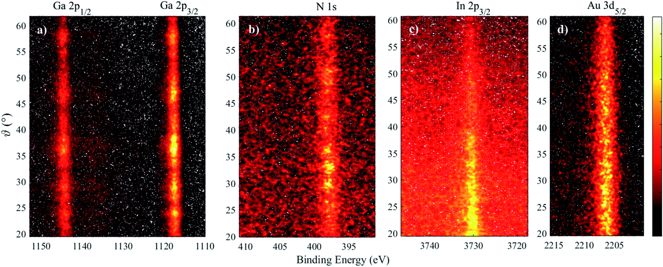 | ||
| Fig. 3 2D angle-resolved data for an InGaN/GaN heterostructure (In fraction of 19%) and a gold reference sample, measured using the AR56 detection mode on the EW4000 analyser. (a) Ga 2p, (b) N 1s, (c) In 2p3/2, and (d) Au 3d5/2 from the reference sample. Increasing photoemission angle indicates increasing surface sensitivity. The intensity colour bar (arb. units) is shown on the right-hand side. | ||
The 2D data may be converted to a set of spectra at different angles by summing ranges of angles, as previously demonstrated.4 Here, each spectrum at every angle (>260 angles across the useful 40° range) was peak fitted with a single Gaussian, after a simple linear background subtraction across a ∼10 eV binding energy range across the photoelectron peak (judged as satisfactory given the signal-to-noise level of the individual spectra) to extract the BE and peak intensity for the N 1s, Ga 2p3/2, In 2p3/2 and Au 3d5/2 photoelectron peaks, and plots of intensity vs. angle and BE vs. angle were compiled. The N, Ga, and In intensity plots were then normalized using the response from the gold reference to remove the natural loss of photoelectron signal with angle, as well as the analyser/detector response.
Fig. 4 shows the BE position, which is defined as the mean of the peak Gaussian fit, of Ga 2p3/2, N 1s and In 2p3/2 for these two heterostructures as a function of the photoemission angle, where a greater angle indicates a lower sampling depth. The Ga 2p3/2 peak shifts to a higher BE by ∼0.7 eV in both samples, indicative of the surface band bending in the n-type GaN capping layer.24 The magnitude of this BE shift is relatively large over the sampling depths probed here, but this is in agreement with previous work and reflects the relatively high electric fields present in these structures.24,25 The N 1s BE position shows a slightly reduced BE shift, however, the relatively low cross section of N 1s compared to Ga 2p means that the signal-to-noise level, even after extracting the parameters via peak fitting, is poor. The slopes of these BE variations were extracted, and found to be similar for Ga 2p3/2 (12 and 13 meV °−1 for x = 0.15 and 0.19, respectively) and N 1s (11 and 18 meV °−1 for x = 0.15 and 0.19, respectively), with a much larger associated error for N 1s. The In 2p3/2 peak may also show some shift in BE position, as much as Ga and N (∼11 meV °−1). However the signal-to-noise level deteriorates with increasing photoemission angle, as less In is detected from the buried layer as the sampling depth is reduced, meaning it is difficult to draw conclusions from photoemission angles above ∼40°. The full-width at half maximum (FWHM) of the fitted peaks was also found to increase with photoemission angle; for Ga 2p3/2 the increase was from ∼1.3 eV at 20° to ∼1.5 eV at 60°, and the other peaks increased by a similar amount (15%). We have therefore assessed band bending through the GaN capping layer and QW and, although the equilibrium band bending will be larger than the measured BE shifts (as the depletion layer is not fully probed), the measurements demonstrate that band bending within a structure may be measured using angle-resolved HAXPES. Further work in this area will include using laser photoexcitation, delivered into the ultra-high-vacuum chamber via calcium fluoride windows for high ultra-violet transmission, to create carriers in the QW as changes to the band bending are monitored.
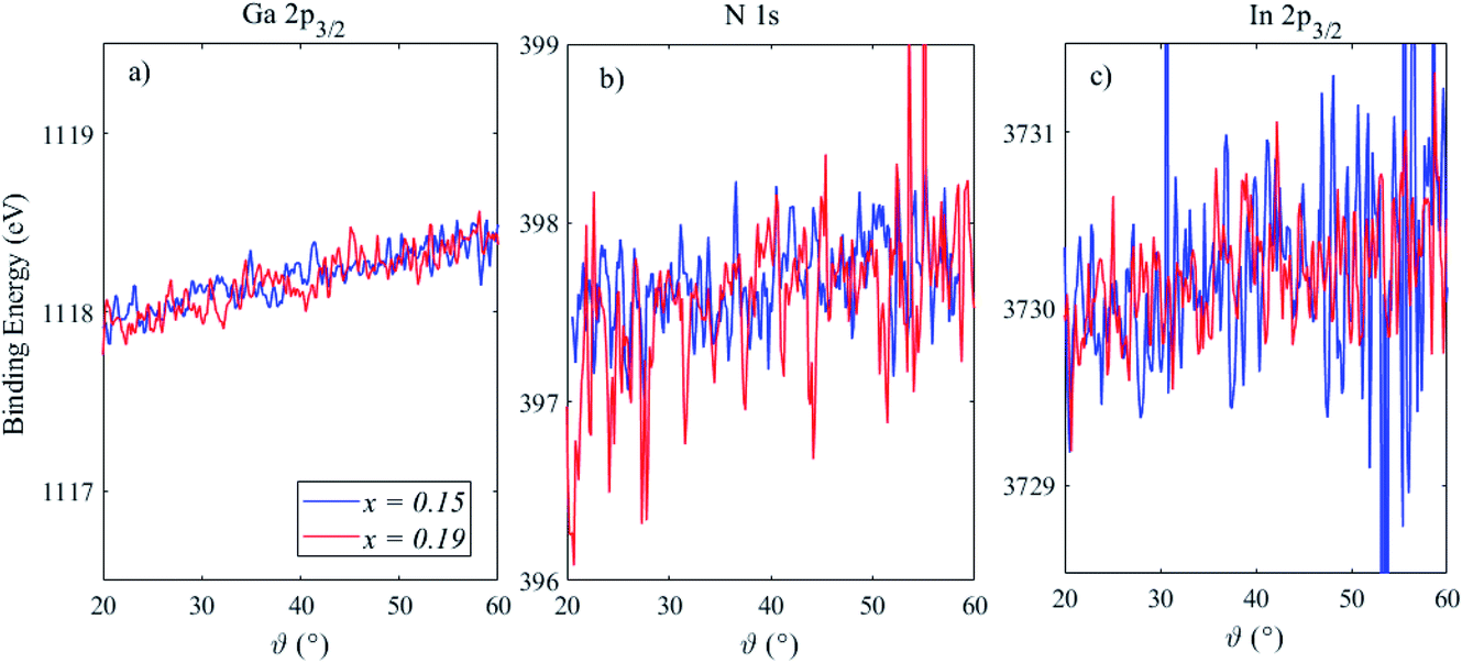 | ||
| Fig. 4 Angle resolved HAXPES measurements of the binding energy peak positions of (a) Ga 2p3/2, (b) N 1s and (c) In 2p3/2 in two InGaN/GaN heterostructures containing 15% In (blue lines) and 19% In (red lines). Increasing the photoemission angle provides greater surface sensitivity. The binding energy scale ranges have been fixed for comparison. | ||
The photoelectron peak intensities (the area below the Gaussian peak fit to the spectra), normalized using the gold reference sample response, for Ga 2p3/2, N 1s and In 2p3/2 are shown in Fig. 5. Undulations are particularly clear for Ga 2p3/2, as observed in the 2D plot in Fig. 3, and these are not removed after normalising using the gold reference response, indicating that they arise from elastic scattering effects, including photoelectron diffraction.37–39 The structure of the normalised Ga 2p3/2 intensities is different in the two samples, which suggests that the azimuthal angles with respect to the crystal planes were different (as expected, since the samples were arbitrarily mounted on the sample plate). Further development may enable the extraction of structural information: for instance, a manipulator with azimuthal rotation could enable diffractograms to be generated which can then be modelled using multiple scattering cluster (MSC) simulations.37–39 Indeed, it is well known that using higher photoelectron kinetic energies (>500 eV) simplifies the analysis of diffractograms due to the so-called “forward focussing” effect, in which emission is enhanced along densely packed atomic planes and rows of atoms corresponding to low-index crystal directions.38,40
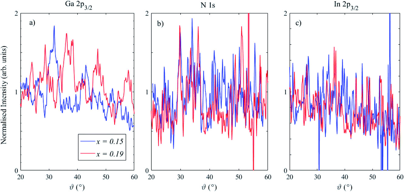 | ||
| Fig. 5 Angle-resolved HAXPES photoelectron peak intensities (normalized using a gold reference sample) for (a) Ga 2p3/2, (b) N 1s and (c) In 2p3/2 in two InGaN/GaN heterostructures containing 15% In (blue lines) and 19% In (red lines). A higher photoemission angle indicates a lower sampling depth. | ||
Disregarding these scattering effects, Ga and N core levels do not show any notable trend in intensity with photoemission angle. The In 2p3/2 intensity plots, in contrast, show a reduction at higher photoemission angles, as expected for a buried layer. These angle-dependent intensity plots may also be used to extract information about the depth distribution of the elements through modelling in software packages such as QUASES-ARXPS.41–43 Analysis of the In angle-resolved data again indicated that some additional contamination was present at the surface, and also that the GaN capping layer was not fully covering the QW structure below, which is expected due to the potential removal of some of the capping layer with ion etching, as well as the presence of V-shaped pits on the surface.
3.2. Characterisation of thin films with capping layers: MnAl for spintronics
Extending the development of spintronics to new devices will require discovery and innovation in magnetic thin film materials.44 The requirements are exacting because the materials must possess high magnetisation and Curie temperatures, very high magnetic anisotropy and, for applications involving magnetisation dynamics, a very low damping parameter. Creating materials with these desirable properties requires a deep understanding of physical properties, including composition, crystal and grain structure, and film thickness.44 These then inform the understanding of magnetic, electrical and dynamic properties. Of the potential candidate materials for future spintronic technologies, binary alloys with an L10 structure show considerable promise. The L10 structure is a distorted fcc structure, so-called face centred tetragonal (fct), where alternating layers of the two constituent atoms form the desired structure, leading to a large magneto-crystalline anisotropy along the tetragonal axis. As alternating layers of atoms are a prerequisite, it follows that L10 binary alloys can only form for equiatomic compositions. A number of equiatomic binary alloys are known to form the L10 structure (FePt, FePd, NiFe, MnAl, CoPt),45 of which the most well-known is FePt.46One L10 binary alloy with potential for spintronic applications is MnAl. Neither Mn or Al show ferromagnetic ordering, however, when combined under the correct thermodynamic conditions (deposition and annealing temperatures) and an appropriate substrate template, the alloy provides magnetic properties similar to those of FePt.47,48 Such properties are normally only found in materials containing 4f elements such as Pt. In the case of MnAl, these desirable magnetic properties are only obtained over a small (∼10%) atomic composition window due to a complex phase diagram, hence a detailed understanding of composition is essential in developing these thin film materials.44 In recent years, there have been relatively few reports on the fabrication of thin film MnAl due to the difficulties in creating the appropriate thermodynamic conditions and ensuring the correct stoichiometry. Here, we show the capability of HAXPES to provide key compositional information in films that are only 50 nm thick. The thin films were fabricated by magnetron sputtering, co-deposited from elemental Mn and Al targets, to understand phase formation of a ∼50 nm MnAl film. To prevent contamination and oxidation, a 5 nm capping layer of Ta was deposited on top of the film. The film and capping layer thicknesses are routinely measured using X-ray reflection measurements, and standard protocols have been developed to enable consistent depositions.
Although the capping layer is very thin, it is thick enough to prevent characterisation with traditional Al Kα XPS, where the sampling depth (defined as three times the inelastic mean free path of electrons) for the Mn 2p core level is ca. 4.5 nm in Ta,10 meaning a 5 nm capping layer is sufficient to prevent sampling of the MnAl material below. The MnAl films are themselves thin at ∼50 nm, which in turn limits characterisation with other techniques, such as inductively-coupled plasma (ICP) etching49 and bulk-sensitive X-ray fluorescence.50 HAXPES with Ga Kα X-rays increases the XPS sampling depth to 27.9 nm for Ta using Mn 2p,10 and the equivalent sampling depth through MnAl is estimated to be similar (33 nm),10 meaning that the MnAl layer is easily measured. The sampling depth does not exceed the total film thickness, hence the calculated relative sensitivity factors for each core level,4,31 assuming a ‘thick’ sample (thickness > sampling depth), may be used to accurately measure the atomic concentrations of Mn and Al in the thin film. For this material system, HAXPES is therefore an ideal probe of the atomic makeup of the thin films beneath a capping layer.
A set of MnAl thin films was fabricated, as detailed above, where the power applied to each target was varied, as detailed in Table 2. This set of spectra for one sample required an accumulation time of ca. 2.5 hours, demonstrating that the flux of the Ga Kα X-ray source is sufficient to enable measurements with similar throughput times to those of traditional Al Kα laboratory instruments. The survey spectrum in Fig. 6(a) shows that, while the intensity of Ta photoelectron peaks is still relatively high, the Mn and Al peaks are easily measurable. These conductive samples did not require the use of a charge neutraliser and, hence, energy calibration was performed using a gold reference sample. The Mn 2p3/2 peak is at BE 638.5 eV, as expected for the metallic phase of Mn,51 as well as MnAl alloys,52 and the spectra indicate little (if any) oxidation, as expected when the film has been capped with Ta. The Mn 1s peak is at 6537.5 eV BE. The Al 2p peak is obscured by Ta 5s, hence the Al 2s peak was measured, and was found to be at 117.0 eV BE, also as expected for metal phase Al,53 with the Al 1s peak position at 1558.8 eV, again as expected for metal phase Al, in agreement with measurements by Castle et al. using Si Kα X-rays.54
| Sample | Mn power (W) | Al power (W) | Expected Mn composition (at%) | Mn at%, Mn 1s, Al 1s, ±0.2 at% | Mn at%, Mn 2p, Al 2s, ±0.6 at% |
|---|---|---|---|---|---|
| a For samples D–H, Mn 2p and Al 2s were not measured with high resolution; the intensity was instead extracted from the survey spectra, and so the error associated with these compositions is significantly greater (estimated to be ∼1.0–2.0 at%) | |||||
| A | 40 | 40 | 50.00 | 50.1 | 51.5 |
| B | 40 | 55 | 42.11 | 27.0 | 38.8 |
| C | 40 | 80 | 33.33 | 33.4 | 27.8 |
| D | 30 | 30 | 50.00 | 53.4 | 49.8a |
| E | 30 | 45 | 40.00 | 40.3 | 46.8a |
| F | 30 | 60 | 33.33 | 31.5 | 25.2a |
| G | 20 | 25 | 44.44 | 47.8 | 37.3a |
| H | 20 | 35 | 36.36 | 25.9 | 24.8a |
| I | 20 | 45 | 30.77 | 34.7 | 29.0 |
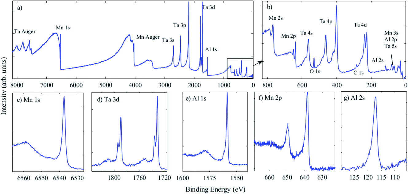 | ||
| Fig. 6 (a) HAXPES survey spectrum, with the inset of (a) shown in (b) showing the low binding energy region, and high resolution spectra of (c) Mn 1s, (d) Ta 3d, (e) Al 1s, (f) Mn 2p and (g) Al 2s from a co-deposited MnAl thin film capped with a ca. 5 nm Ta surface layer. Measurements were performed with grazing incidence in transmission mode. | ||
Now that HAXPES technology has developed, particularly in the laboratory environment where a variety of X-ray sources are available,2 an update of reference data will increase confidence in the chemical states identified using deeper core levels. The Ta 3d5/2 photoelectron peak is present at 1731.8 eV BE, and is in agreement with the literature.55 Here, however, an additional peak is present at an approx. 4.4 eV higher BE and assigned to the oxide, accounting for ca. 16% of the signal. As Ta readily oxidises, this is expected given that the Ta capping layer was exposed to the atmosphere. This chemical shift is similar to that observed for Ta 4f7/2 in the metallic phase and in Ta2O5 using XPS.56,57 While BE positions for deeper core levels than those used in XPS (BE > 1500 eV) are less widely available, it is anticipated that chemical shifts may generally be consistent with those from traditional XPS measurements. Additional peaks across the range 3500–4200 eV BE in the survey spectrum are assigned to Mn Auger peaks, but again, a definitive assignment from the literature is lacking as they occur at relatively high kinetic energies (>5 keV). Measurement of these Auger peak positions, again with further reference data, may also enable chemical state information to be extracted using HAXPES, using the Auger parameter, as for XPS,58,59 and as recently demonstrated using HAXPES.60
Table 2 shows that there is generally good agreement between the measured composition and the expected composition (based on the ratio of the Mn and Al target powers, anticipating a linear relationship between the composition and target). Errors were estimated using the calculated relative changes in at%, as previously detailed in section 3.1 of the Results.
Two notable discrepancies are samples B and H, which also show relatively high inelastic backgrounds (i.e., lower intensity primary photoelectron peaks), particularly for Mn 1s, as shown in Fig. 7. The survey spectra for these two samples show a higher amount of Ta than those of the other samples, meaning the capping layer was thicker in these samples. The Mn 1s photoelectrons have a lower kinetic energy than Al 1s (and are thus associated with a lower sampling depth); it may be in these cases the use of Mn 1s is not appropriate, and indeed for sample B, the measured composition using Mn 1s and Al 1s core levels is 27% Mn, much lower than the expected 42%. As can be seen from Table 2, use of the Mn 2p and Al 2s signals (at much higher and similar kinetic energies) gives a composition of 39% Mn, which is not significantly different from the expected value. Sample H, however, shows a similar Mn composition measured with both sets of core levels (∼25%), lower than the expected value of 36%. These data were extracted using the survey spectrum, with a much greater associated error. Overall, for the majority of samples with thinner capping layers, there is good agreement between the Mn compositions extracted using the two sets of core levels at higher and lower binding energies, which adds to the confidence in the calculated RSFs.
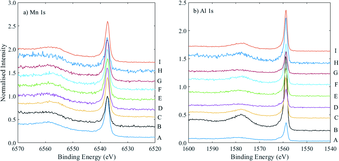 | ||
| Fig. 7 (a) Mn 1s, and (b) Al 1s spectra, normalised to the Mn 1s peak intensity and offset on the y-axis, for a set of samples A–I, as labelled, where the powers of the Mn and Al targets were varied, as listed in Table 2. | ||
These results demonstrate the capability to measure material composition and chemical states below top electrode layers in electrical devices. They also demonstrate that capping vacuum-deposited materials with a metal layer at the surface can prevent atmospheric exposure without prohibiting the analysis of the material of interest via photoelectron spectroscopy with hard X-rays.
3.3. The metal oxide interface in zirconium
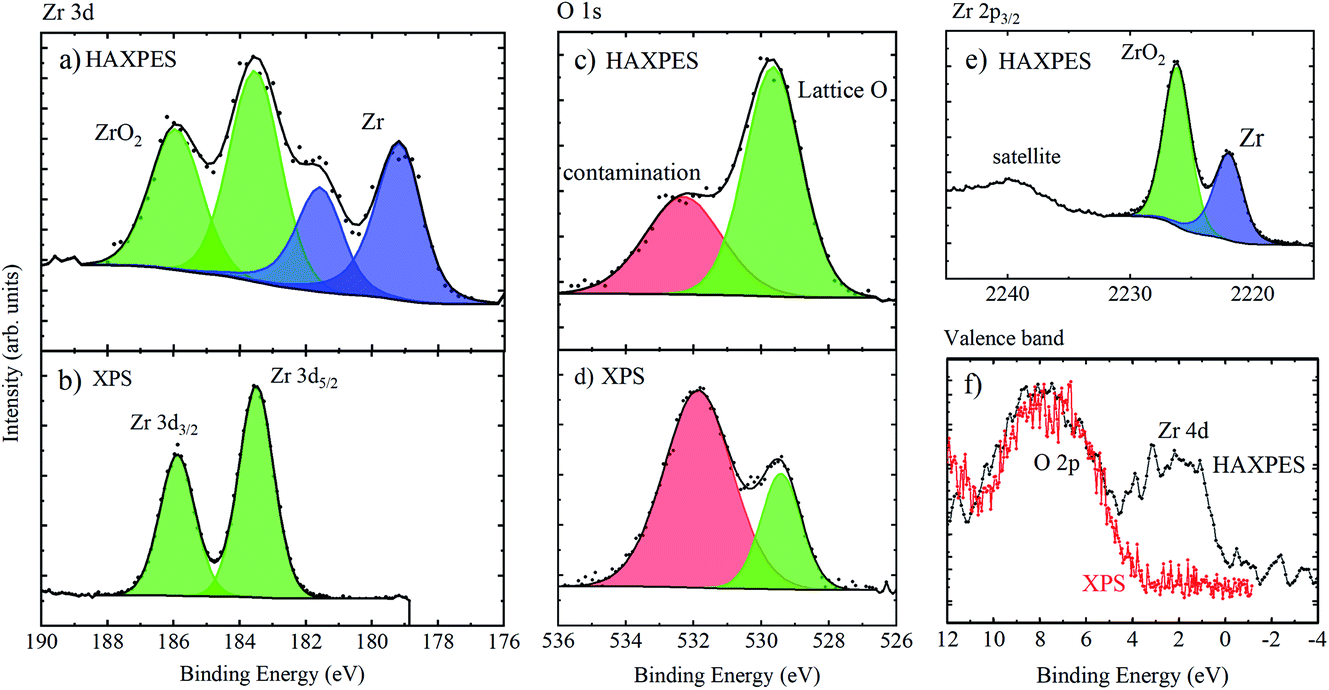
The surface of zirconium, like many metals, exhibits an oxide passivation layer. Zirconium dioxide itself has been extensively studied for applications in fuel cells, gas sensors, as a coating, and in metal-oxide semiconductor devices.61 Metallic Zr can readily form a surface oxide layer even at low temperatures and in relatively low oxygen environments,62 therefore the characterisation of the electronic properties of zirconium and its oxides is important for a number of sectors. Here, we examine a piece of untreated Zr metal, left exposed to the atmosphere for a prolonged period, measured using surface sensitive XPS and HAXPES.Fig. 8 shows the survey spectra of untreated Zr metal measured using HAXPES and XPS, with the inset showing the Zr LMM Auger features at ∼1850 eV kinetic energy and an enhanced view of the region below 1200 eV BE. The relative changes in the photoionisation cross sections are clear here, shown by the relative intensity of Zr 3d compared with the Zr 3p and 3s intensities in the XPS and HAXPES spectra: the relative intensity of the Zr 3d photoelectron line is diminished in the HAXPES spectrum due to a relative decrease in the photoionization cross section. The HAXPES survey spectrum shows much greater sensitivity to deeper core levels; the intensities of Zr 2s and 2p are an order of magnitude greater than those of 3s, 3p, and 3d.
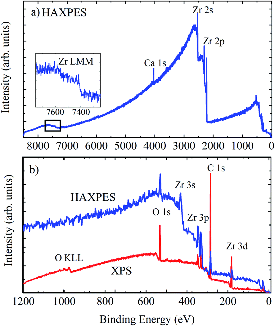 | ||
| Fig. 8 (a) HAXPES survey spectrum of an untreated piece of Zr metal (inset shows the Zr LMM Auger region), and (b) overlay of HAXPES (blue line) and XPS survey (red line) spectra up to 1200 eV binding energy. | ||
Fig. 9 shows the high resolution spectra of Zr 3d, Zr 2p, O 1s and the valence band regions of the untreated Zr sample. As expected, the surface sensitive XPS spectrum of Zr 3d shows one spin–orbit split chemical species, with Zr 3d5/2 at 183.5 eV BE associated with ZrO2.62 HAXPES, however, shows two species; a second doublet is present at ca. 4.4 eV lower binding energy (Zr 3d5/2 at 179.1 eV), associated with metallic Zr.62 Similarly, the Zr 2p3/2 peak is comprised of two chemical species (the doublet pair is not shown as the spin–orbit splitting of Zr 2p is relatively large). The BEs of the metallic and oxide species are 2221.9 and 2226.2 eV, respectively, meaning a chemical shift of 4.3 eV, similar to the Zr 3d chemical shift. References for deeper core levels such as Zr 2p3/2 are very few, but the metallic BE position measured here is the same within error as that measured by Huschka et al. using Ag Lα and Ti Kα X-rays (not monochromated) on a Kratos XSAM 800 spectrometer from Zr foil, cleaned in situ by scratching (2222.2 ± 0.4 eV).55 The O 1s spectra show a greater proportion of lattice oxygen (measured at a lower binding energy, here ∼529 eV) when measured with HAXPES, because there is lower sensitivity to oxygen-containing contamination (such as hydroxides and oxidised carbon species) at the surface. Finally, the valence band spectra show that HAXPES, sampling the metallic Zr below the oxide passivation layer, measures the Zr 4d core level at a low binding energy.61,63
 | ||
| Fig. 9 Zr 3d spectra of an untreated piece of Zr metal, measured using (a) HAXPES (9.25 keV) and (b) XPS (1.486 keV), O 1s spectra measured with (c) HAXPES and (d) XPS, (e) Zr 2p3/2 spectra measured using HAXPES, and (f) valence band spectra measured using HAXPES (black points and line) and XPS (red points and line). | ||
The measured ratio of metallic to oxidised zirconium changes depending on whether Zr 3d or 2p photoelectrons are used, due to a change in the sampling depth of the photoelectrons, as the kinetic energy difference is ca. 2 keV. According to the TPP-2M formula,64 and assuming that the majority of the photoelectrons are travelling through ZrO2, the sampling depths for Zr 3d and 2p are 32 and 26 nm, respectively (calculated using eqn (1)). In comparison, XPS using Zr 3d has a calculated sampling depth of 7 nm. A simple calculation may be made to obtain the oxide layer thickness, using the ratio of metallic:oxide Zr 3d or 2p3/2 signals, an assumed stoichiometry of the oxide layer (Zr:O = 1:2), and assuming both a uniform and abrupt overlayer and identical shake-up intensity for all core-level peaks. The Strohmeier equation gives the relation for the oxide layer thickness, d:65
 | (2) |
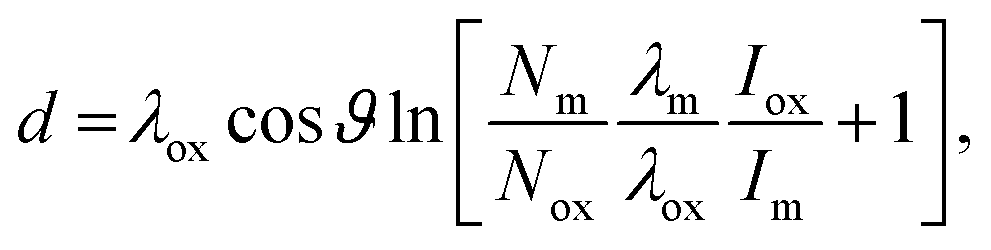
The sample was heated in situ; at temperatures approaching 373 K, a large increase in vacuum pressure associated with the removal of surface contamination occurred, after which the vacuum dropped to <2 × 10⁻⁸ mbar (2 × 10⁻⁶ Pa), which is suitable for measurement. The Zr 2p3/2 core level was then monitored as a function of increasing temperature, as illustrated in Fig. 10. The temperature was monitored using a K-type thermocouple attached to the base of the manipulator, and for temperatures over 493 K, a further calibration between the measured and sample temperature was required as provided by the manufacturer of the instrument. There is little change in the relative intensity of oxide and metal features up to temperatures of 473 K, but at 673 K the oxide is largely removed, and completely removed by 893 K. This confirms that the high BE species is associated with the oxide passivation layer. The complete removal of the oxide overlayer also allowed the extraction of the asymmetric metallic peak shape required for peak fitting and quantification of the data from the oxidised films.
 | ||
| Fig. 10 Zr 2p3/2 spectra of a piece of untreated Zr metal which was heated from room temperature (a) to 893 K (e). | ||
3.4. Ion implantation in graphite
Implantation of charged species into the matrix of a material is an area of interest in many research fields.66–69 Here, we examine highly oriented pyrolytic graphite (HOPG) implanted with Cs+ ions. Caesium is a by-product of uranium fission and is known to be potentially mobile under certain conditions,70,71 and HOPG is commonly used as a nuclear graphite simulant.72 Therefore, sensitive methods to measure caesium distributions are useful. A sample of the simulant HOPG was implanted with 50 keV Cs+ ions and then exposed to the atmosphere, as described elsewhere.73 The ion beam was 50 μm in diameter and was rastered across the surface of the HOPG. SRIM calculations (stopping and range of ions in matter)74 suggested that the ions should implant as a Gaussian distribution centred below the surface of the HOPG, at a depth of ca. 20 nm, and, consistent with this, initial measurements with Al Kα XPS detected a small amount of Cs.73 However, subsequent XPS imaging revealed that the rastering had not yielded a uniform distribution of Cs across the sample, possibly implying lateral variations in the ion implantation depth distribution.73 Insight into variations in the ion implantation depth distribution across the HOPG surface was therefore required and was enabled using HAXPES and inelastic background modelling using the Cs 2s and 2p core levels.Inelastic background modelling, pioneered by Sven Tougaard,75 and implemented in the QUASES-Tougaard software package,76 makes use of the energy loss structure to lower kinetic energy from a primary photoemission peak. Inspection of the inelastic background (where electrons are scattered with associated energy loss) can be used to provide a signature of the morphology of that element below the surface: indeed, a simple visual inspection of the core levels and the background in a survey spectrum yields useful insight into the morphology.77 A recent publication also provides an important practical guide to carrying out this analysis.78 The ultimate depth from which information may be extracted depends on the measurable kinetic energy range of this energy loss structure, i.e., the width of the range to high binding energy from a primary photoelectron emission peak that is unperturbed by any peaks due to other elements.79 For XPS, where multiple core levels are often present within a relatively small binding energy range, together with Auger peaks, the information depth can be somewhat limited. However, HAXPES enables the use of deeper core levels, typically separated from other photoemission peaks by much greater energy intervals.4 We have shown that, even after the complete loss of the elastic photoelectron signal, the depth of a buried element may still be extracted at up to 20 times the electron attenuation length, corresponding to hundreds of nm.4
This inelastic background modelling is well established and has been refined to take into account elastic scattering effects, layered structures with greatly differing cross sections and electron attenuation lengths.80,81 Accuracy and depth resolution is generally improved using reference samples.4,82 Background analysis also has the potential to correct for the effect of photoelectron attenuation through a gaseous atmosphere in near ambient pressure (NAP) XPS measurements.83 Here, we simply demonstrate how dramatically the inelastic background is influenced by the morphology of the sample, using a sample of HOPG that has been implanted with Cs+ ions.
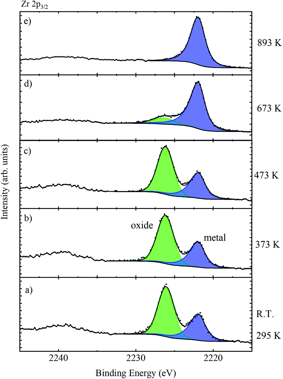
Measurements were performed at grazing incidence in transmission mode, across the Cs 2s, 2p region. A range of several hundred eV to the high kinetic energy of the Cs 2p3/2 peak was used to carefully remove the preceding background, and the spectrum was measured over several hundred eV to the lower kinetic energy of the Cs 2s and 2p peaks. The inelastic mean free path of electrons was calculated to be 8.9 nm using the TPP-2M formula,10 using the QUASES-TPP2M calculator tool, assuming that the photoelectrons are mainly travelling through graphite. Analysis was performed using the QUASES-Tougaard-Analyze software, which is applicable when the elastic photoelectron peaks are observable.78 Several elemental distribution models are available in the software, including an exponential profile into or out of the bulk material, however, here it was found that a simple buried layer model was sufficient to adequately model the background shapes, and this provided insight into the caesium distributions following implantation.
Fig. 11 shows the Cs 2s, 2p spectra taken at six positions across the HOPG sample, from the centre of the 10 mm × 10 mm sample to 5 mm away from the centre laterally in one direction, which was very close to the edge of the HOPG sample. The Cs 2p3/2 core level peak is at 5011.0 eV BE, and the Cs 3d5/2 core level signal was measured at 724.8 eV BE. The relative intensities of the primary peaks (from elastic processes) and secondary background features (from inelastic scattering) depend on the depth distribution and sampling depth associated with the peak. From a visual inspection of the inelastic backgrounds, it is clear that the depth distribution of Cs atoms embedded in the graphite changes with lateral distance away from the centre of the sample. Only at 4 mm and 5 mm away from the centre do the Cs peaks show large rising inelastic backgrounds to low KE from each photoelectron peak that exceed the primary photoelectron peak intensity, indicating that the Cs is heavily buried. The process of ion implantation is expected to damage the graphitic carbon matrix, particularly when high concentrations of ions are implanted; that damage may lead to the loss of graphite at the surface during implantation and may also allow for an enhancement in the mobility of the Cs ions after implantation. The amount of Cs measured (using the Cs 2p3/2, C 1s, and O 1s photoelectron peaks) varied significantly from ca. 11 at% (equivalent homogeneous concentration) at the centre, down to ca. 1 at% 5 mm away from the centre.
 | ||
| Fig. 11 HAXPES inelastic background modelling of Cs+ ions implanted in HOPG for distances up to 5 mm away from the centre of the sample, as labelled. Data are shown by blue lines, the background model is shown by red lines, and the difference is shown by green lines. The backgrounds were modelled as buried layers (thicknesses ranging from 10–20 nm) at a starting depth of 9 nm (0 mm from the sample centre), 15 nm (1 mm), 17 nm (2 mm), 20 nm (3 mm), 22 nm (4 mm) and 30 nm (5 mm). | ||
The changes in the spectra close to the sample centre suggest some removal of surface material due to implantation. The background models used to fit the data were all generated with a buried layer with a thickness of 10–20 nm. In order to model the possible effects of implantation, the starting depth of this buried layer was varied and optimized in order to adequately fit the data. It was found that from 0 to 5 mm from the sample centre, the best fits were obtained for buried layer starting depths of 9 nm, 15 nm, 17 nm, 20 nm, 22 nm, and 30 nm, respectively, consistent with SRIM calculations and a varying degree of lost surface materials, except for the measurement at the sample edge, where the calculated starting depth exceeded the SRIM model expectation. Alternatively, some ion migration could be occurring through the damaged carbon matrix at room temperature, or there is a combination of these effects; further investigation is planned.
Inelastic background analysis therefore provides another important tool for the characterisation of buried interfaces; overall, this analysis, where applicable, is more efficient than analogous angle-resolved measurements, as detailed in section 3.1 of the Results. However, for high accuracy, great care must be taken when determining the input parameters used in the analysis.78
3.5. Detection of nanoparticle cores under thick shells
Nanoparticles commonly have an internal structure which typically consists of layers, or shells, around a functional core. The purpose of the shell material may be protective, functional, or accidental. Examples of protection include the passivation of luminescent quantum dots for optoelectronic and bioimaging or a layer forming a diffusion barrier in drug-eluting particles where the active ingredient is centrally located. Functional coatings are usually designed to interact with the particle environment to aid particle dispersion, prevent adsorption of molecules (for example polyethylene glycol coatings to reduce protein attachment), or to provide targeted adhesion. The measurement of the average coating thickness and information on the elemental depth distributions in a population of particles can be performed using XPS, however the data analysis must consider the geometry of the particles. For large particles with a uniform coating, the signal intensity from the underlying material is approximately 2/3 that of a flat surface with the same coating thickness.84 This implies that the information depth for particles should be estimated as twice the effective attenuation length (EAL) of electrons, rather than three times, as is typical for flat surfaces. For nanoparticles, where the dimension of the particle is similar to the EAL, there is a further drop in intensity from the core material, particularly for thick shells. With some knowledge of particle sizes and the internal distribution of materials in the particles, XPS data can be analysed to provide shell thicknesses and compositions.85–88Due to the constraints described above on the depth information from XPS, HAXPES may be a suitable technique for the analysis of particles with small cores and thick shells. A series of reference nanoparticles with a PTFE core and PMMA shell have been analysed by a wide range of methods, including XPS.89,90 For these particles, which possess a 47 nm diameter core and nominal shell thicknesses of 4.5 nm, 12 nm, 23.5 nm and 35.5 nm, Al Kα XPS was only able to reliably detect the F 1s peak from the PTFE core material for the three smallest particles. In the case of the nominal 12 and 23.5 nm shell thicknesses, this detection was possible because of the non-central location of the cores within these particles.89 For the largest particle type (with a shell thickness of 35.5 nm), the core could not be detected and sputter depth profiling using argon cluster ions was necessary to obtain detail on the internal distribution of the materials.91
Fig. 12(a) and (b) demonstrate that the core material may be detected for particles with nominal shell thicknesses of 12 nm, 23.5 nm and 35.5 nm using Ga Kα HAXPES. For the thickest shell, the F 1s signal is close to the detection limit; equivalent homogeneous concentrations of the F at% were calculated to be 24.4, 7.2 and 2.2 at%, respectively. In this case, it must be considered that the PTFE core is buried, on average, under more than 30 nm of PMMA and the volume fraction of PTFE in the core–shell particles is less than 5%, therefore this is a significant achievement for a light element with a low photoionisation cross-section. The graph in Fig. 12(c) illustrates the measured fluorine atomic fractions from XPS and HAXPES for these samples. Solid lines represent the expected intensities with a centrally located core and the dashed lines are the expected orientation-averaged intensities for a non-central core located 3 nm beneath the particle surface (as illustrated in the schematic in Fig. 12(d), where the displacement below the surface is labelled “D”). This ‘off-centre’ model is based upon transmission electron microscopy analysis,89 and approximately describes the XPS and HAXPES data. Divergences indicate that for smaller particles, the cores are slightly closer to the surface than 3 nm, but for the largest particle type the cores are somewhat deeper.
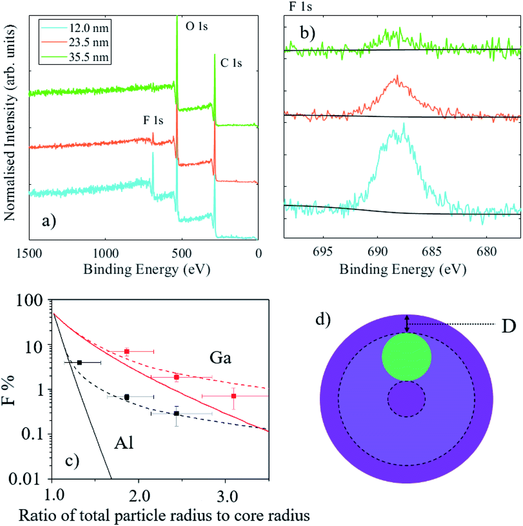 | ||
| Fig. 12 (a) Survey spectra and (b) high resolution F 1s spectra for 12.0 nm, 23.5 nm and 35.5 nm nominal shell thickness PTFE-PMMA core–shell particles (cyan, orange and green lines, respectively). (c) Measured F 1s at% and modelled data. Solid lines indicate the expected fluorine at% for a centralised core, and dashed lines indicate the expected fluorine at% for a core displaced 3 nm from the particle surface, and points indicate measured values. Black lines and points are data corresponding to Al Kα X-rays, whereas red lines and points correspond to Ga Kα X-rays, as indicated. (c) Schematic diagram showing the morphology used for modelling; intensities are averaged for a core located anywhere within the shaded area, where D is the core displacement from the surface. | ||
4. Conclusions
These results showcase measurements on a wide range of material systems containing buried interfaces, with characterisation of the buried layers enabled by hard X-ray photoelectron spectroscopy, extending the traditional XPS sampling depth below the topmost surface. The HAXPES-Lab system from ScientaOmicron GmbH uses an EW4000 analyser with a wide acceptance angle, which also enables angle-resolved measurements, capturing >40° angular information in one shot. The capabilities of the instrument may be usefully combined with advanced analysis techniques, including the modelling of the angle-resolved data, and use of the inelastic background. Taken in combination, these approaches extend the depth-profiling capabilities of HAXPES smoothly from the XPS regime to hundreds of nm below the surface. It is therefore anticipated that research utilising HAXPES will continue to accelerate, especially now that high-throughput measurements are enabled in the laboratory environment, and these methods will be applicable to a wide range of advanced materials research.Author contributions
BFS: conceptualization, data curation, formal analysis, funding acquisition, investigation, methodology, software, validation, visualization, writing – original draft, writing – review & editing. SAC: conceptualization, data curation, formal analysis, investigation, software, validation, visualization, writing – original draft, writing – review & editing. PT: data curation, formal analysis, investigation, methodology, investigation, resources, writing – original draft, writing – review & editing. DJHC: conceptualization, data curation, formal analysis, methodology, resources, software, validation, visualization, writing – original draft, writing – review & editing. SM: investigation, methodology, validation, writing – review & editing. AT: conceptualization, investigation, methodology, resources, writing – original draft, writing – review & editing. ANJ: conceptualization, resources, supervision, writing – review & editing. MJK: resources. DJB: conceptualization, resources, supervision, validation, writing – review & editing. RAO: conceptualization, resources, supervision, validation, writing – review & editing. JH: conceptualization, data curation, methodology, resources, validation, writing – review & editing. AGT: conceptualization, supervision, writing – review & editing. TT: conceptualization, resources, validation, supervision, writing – original draft, writing – review & editing. AGS: conceptualization, data curation, formal analysis, funding acquisition, methodology, software, supervision, visualization, writing – original draft, writing – review & editing. WRF: conceptualization, funding acquisition, methodology, supervision, validation, writing – review & editing.Conflicts of interest
There are no conflicts to declare.Acknowledgements
This work was supported by the Henry Royce Institute for Advanced Materials, funded through the EPSRC grants EP/R00661X/1, EP/P025021/1 and EP/P025498/1, and the National Measurement System of the UK Department of Business, Energy and Industrial Strategy (BEIS).Notes and references
- J. Woicik, Hard X-ray Photoelectron Spectroscopy (HAXPES), Springer International Publishing, Cham, 2016 Search PubMed.
- C. Kalha, N. K. Fernando, P. Bhatt, F. O. L. Johansson, A. Lindblad, H. Rensmo, L. Z. Medina, R. Lindblad, S. Siol, L. P. H. Jeurgens, C. Cancellieri, K. Rossnagel, K. Medjanik, G. Schonhense, M. Simon, A. X. Gray, S. Nemsak, P. Lomker, C. Schlueter and A. Regoutz, J. Phys.: Condens. Matter, 2021, 33, 233001 CrossRef CAS PubMed.
- A. Regoutz, M. Mascheck, T. Wiell, S. K. Eriksson, C. Liljenberg, K. Tetzner, B. A. D. Williamson, D. O. Scanlon and P. Palmgren, Rev. Sci. Instrum., 2018, 89, 073105 CrossRef PubMed.
- B. F. Spencer, S. Maniyarasu, B. P. Reed, D. J. H. Cant, R. Ahumada-Lazo, A. G. Thomas, C. A. Muryn, M. Maschek, S. K. Eriksson, T. Wiell, T. L. Lee, S. Tougaard, A. G. Shard and W. R. Flavell, Appl. Surf. Sci., 2021, 541, 148635 CrossRef CAS.
- M. B. Trzhaskovskaya and V. G. Yarzhemsky, At. Data Nucl. Data Tables, 2019, 129–130, 101280 CrossRef CAS.
- M. B. Trzhaskovskaya and V. G. Yarzhemsky, At. Data Nucl. Data Tables, 2018, 119, 99–174 CrossRef CAS.
- S. Maniyarasu, J. C. Ke, B. F. Spencer, A. S. Walton, A. G. Thomas and W. R. Flavell, ACS Appl. Mater. Interfaces, 2021, 13, 43573–43586 CrossRef CAS PubMed.
- M. Bouttemy, S. Béchu, B. F. Spencer, P. Dally, P. Chapon and A. Etcheberry, Coatings, 2021, 11, 702 CrossRef CAS.
- A. Theodosiou, B. F. Spencer, J. Counsell and A. N. Jones, Appl. Surf. Sci., 2020, 508, 144764 CrossRef CAS.
- H. Shinotsuka, S. Tanuma, C. J. Powell and D. R. Penn, Surf. Interface Anal., 2015, 47, 871–888 CrossRef CAS.
- A. Regoutz, M. Mascheck, T. Wiell, S. K. Eriksson, C. Liljenberg, K. Tetzner, B. A. D. Williamson, D. O. Scanlon and P. Palmgren, Rev. Sci. Instrum., 2018, 89, 73105 CrossRef PubMed.
- D. H. Larsson, P. A. C. Takman, U. Lundström, A. Burvall and H. M. Hertz, Rev. Sci. Instrum., 2011, 82, 123701 CrossRef CAS PubMed.
- A. Thompson, D. Attwood, E. Gullikson, M. Howells, K.-J. Kim, J. Kirz, J. Kortright, I. Lindau, Y. Liu, P. Pianetta, A. Robinson, J. Scofield, J. Underwood, G. Williams and H. Winick, X-ray Data Booklet, Lawrence Berkeley National Laboratory, Berkeley, CA 94720, United States, 2009 Search PubMed.
- Q. Lian, M. Z. Mokhtar, D. Lu, M. Zhu, J. Jacobs, A. B. Foster, A. G. Thomas, B. F. Spencer, S. Wu, C. Liu, N. W. Hodson, B. Smith, A. Alkaltham, O. M. Alkhudhari, T. Watson and B. R. Saunders, ACS Appl. Mater. Interfaces, 2020, 12, 18578–18589 CrossRef CAS PubMed.
- P. Dawson, S. Schulz, R. A. Oliver, M. J. Kappers and C. J. Humphreys, J. Appl. Phys., 2016, 119, 181505 CrossRef.
- V. Fiorentini, F. Bernardini, F. Della Sala, A. Di Carlo and P. Lugli, Phys. Rev. B: Condens. Matter Mater. Phys., 1999, 60, 8849–8858 CrossRef CAS.
- S. A. Church, G. M. Christian, R. M. Barrett, S. Hammersley, M. J. Kappers, M. Frentrup, R. A. Oliver and D. J. Binks, J. Phys. D: Appl. Phys., 2021, 54, 475104 CrossRef CAS.
- M. Auf Der Maur, A. Pecchia, G. Penazzi, W. Rodrigues and A. Di Carlo, Phys. Rev. Lett., 2016, 116, 027401 CrossRef PubMed.
- G. Kusch, E. J. Comish, K. Loeto, S. Hammersley, M. J. Kappers, P. Dawson, R. A. Oliver and F. C. P. Massabuau, Nanoscale, 2022, 14, 402–408, 10.1039/d1nr06088k.
- B. F. Spencer, M. J. Cliffe, D. M. Graham, S. J. O. Hardman, E. A. Seddon, K. L. Syres, A. G. Thomas, F. Sirotti, M. G. Silly, J. Akhtar, P. O’Brien, S. M. Fairclough, J. M. Smith, S. Chattopadhyay and W. R. Flavell, Faraday Discuss., 2014, 171, 275–298 RSC.
- B. F. Spencer, M. J. Cliffe, D. M. Graham, S. J. O. Hardman, E. A. Seddon, K. L. Syres, A. G. Thomas, F. Sirotti, M. G. Silly, J. Akhtar, P. O’Brien, S. M. Fairclough, J. M. Smith, S. Chattopadhyay and W. R. Flavell, Surf. Sci., 2015, 641, 320–325 CrossRef CAS.
- B. F. Spencer, D. M. Graham, S. J. O. Hardman, E. A. Seddon, M. J. Cliffe, K. L. Syres, A. G. Thomas, S. K. Stubbs, F. Sirotti, M. G. Silly, P. F. Kirkham, A. R. Kumarasinghe, G. J. Hirst, A. J. Moss, S. F. Hill, D. A. Shaw, S. Chattopadhyay and W. R. Flavell, Phys. Rev. B: Condens. Matter Mater. Phys., 2013, 88, 195301 CrossRef.
- B. F. Spencer, M. A. Leontiadou, P. C. J. Clark, A. I. Williamson, M. G. Silly, F. Sirotti, S. M. Fairclough, S. C. E. Tsang, D. C. J. Neo, H. E. Assender, A. A. R. Watt and W. R. Flavell, Appl. Phys. Lett., 2016, 108, 091603 CrossRef.
- S. Ueda, Appl. Phys. Express, 2018, 11, 105701 CrossRef.
- T. Narita, D. Kikuta, N. Takahashi, K. Kataoka, Y. Kimoto, T. Uesugi, T. Kachi and M. Sugimoto, Phys. Status Solidi A, 2011, 208, 1541–1544 CrossRef CAS.
- G. M. Christian, S. Schulz, M. J. Kappers, C. J. Humphreys, R. A. Oliver and P. Dawson, Phys. Rev. B, 2018, 98, 155301 CrossRef CAS.
- D. M. Graham, A. Soltani-Vala, P. Dawson, M. J. Godfrey, T. M. Smeeton, J. S. Barnard, M. J. Kappers, C. J. Humphreys and E. J. Thrush, J. Appl. Phys., 2005, 97, 103508 CrossRef.
- A. Vanleenhove, C. Zborowski, I. Vaesen, I. Hoflijk and T. Conard, Surf. Sci. Spectra, 2021, 28, 014006 CrossRef CAS.
- DOI:10.1088/0031-8949/22 .
- Y. Kayanuma, in Hard X-ray Photoelectron Spectroscopy (HAXPES), ed. J. Woicik, Springer International Publishing, 2016, pp. 175–195, DOI:10.1007/978-3-319-24043-5_8.
- D. J. H. Cant, B. F. Spencer, W. R. Flavell and A. G. Shard, Surf. Interface Anal., 2022, 54, 442–454 CrossRef CAS.
- P. L. J. Gunter, O. L. J. Gijzeman and J. W. Niemantsverdriet, Appl. Surf. Sci., 1997, 115, 342–346 CrossRef CAS.
- L. P. Kazansky, I. A. Selyaninov and Y. I. Kuznetsov, Appl. Surf. Sci., 2012, 259, 385–392 CrossRef CAS.
- M. P. Seah, J. H. Qiu, P. J. Cumpson and J. E. Castle, Surf. Interface Anal., 1994, 21, 336–341 CrossRef CAS.
- P. J. Cumpson, J. Electron Spectrosc. Relat. Phenom., 1995, 73(1), 25–52 CrossRef CAS.
- V. I. Nefedov, J. Electron Spectrosc. Relat. Phenom., 1999, 100, 1–15 CrossRef CAS.
- A. Chassé and T. Chassé, J. Phys. Soc. Jpn., 2018, 87, 061006 CrossRef.
- L. Despont, D. Naumović, F. Clerc, C. Koitzsch, M. G. Garnier, F. J. Garcia De Abajo, M. A. Van Hove and P. Aebi, Surf. Sci., 2006, 600, 380–385 CrossRef CAS.
- F. J. García De Abajo, M. A. Van Hove and C. S. Fadley, Phys. Rev. B: Condens. Matter Mater. Phys., 2001, 63, 075404 CrossRef.
- H. A. Aebischer, T. Greber, J. Osterwalder, A. P. Kaduwela, D. J. Friedman, G. S. Herman and C. S. Fadley, Surf. Sci., 1990, 239, 261–264 CrossRef CAS.
- T. S. Lassen, S. Tougaard and A. Jablonski, Surf. Sci., 2001, 481, 150–162 CrossRef CAS.
- S. Tougaard, Surf. Interface Anal., 1998, 26, 249–269 CrossRef CAS.
- S. Tougaard and A. Jablonski, Surf. Interface Anal., 1997, 25, 404–408 CrossRef CAS.
- J. Cui, M. Kramer, L. Zhou, F. Liu, A. Gabay, G. Hadjipanayis, B. Balasubramanian and D. Sellmyer, Acta Mater., 2018, 158, 118–137 CrossRef CAS.
- A. Edström, J. Chico, A. Jakobsson, A. Bergman and J. Rusz, Phys. Rev. B: Condens. Matter Mater. Phys., 2014, 90, 014402 CrossRef.
- B. S. D. C. S. Varaprasad, M. Chen, Y. K. Takahashi and K. Hono, IEEE Trans. Magn., 2013, 49, 718–722 CAS.
- X. Zhang, L. L. Tao, J. Zhang, S. H. Liang, L. Jiang and X. F. Han, Appl. Phys. Lett., 2017, 110, 252403 CrossRef.
- S. Zhao, T. Hozumi, P. Leclair, G. J. Mankey and T. Suzuki, IEEE Trans. Mag., 2015, 51, 2101604 Search PubMed.
- Z. Luo, S. Shao and T. Wu, Microelectron. Eng., 2021, 242–243, 111530 CrossRef CAS.
- R. Sitko, Spectrochim. Acta, Part B, 2009, 64, 1161–1172 CrossRef.
- C. J. Jenks, S. L. Chang, J. W. Anderegg, P. A. Thiel and D. W. Lynch, Phys. Rev. B: Condens. Matter Mater. Phys., 1996, 54, 6301–6306 CrossRef CAS PubMed.
- C. Navío, M. Villanueva, E. Céspedes, F. Mompeán, M. García-Hernández, J. Camarero and A. Bollero, APL Mater., 2018, 6, 101109 CrossRef.
- P. M. Th, M. Van Attekum and J. M. Trooster, Phys. Rev. B: Condens. Matter Mater. Phys., 1978, 18, 3872–3883 CrossRef.
- J. E. Castle, L. B. Hazell and R. D. Whitehead, J. Electron Spectrosc. Relat. Phenom., 1976, 9, 247–250 CrossRef CAS.
- W. Huschka, D. Ross, M. Maier and E. Umbach, J. Electron Spectrosc. Relat. Phenom., 1988, 46, 273–276 CrossRef CAS.
- E. Atanassova, T. Dimitrova and J. Koprinarova, Appl. Surf. Sci., 1995, 84, 193–202 CrossRef CAS.
- P. Prieto, L. Galán and J. M. Sanz, Appl. Surf. Sci., 1993, 70–71, 186–190 CrossRef CAS.
- J. E. Castle, Surf. Interface Anal., 2022, 54(4), 455–464 CrossRef CAS.
- C. D. Wagner and A. Joshi, J. Electron Spectrosc. Relat. Phenom., 1988, 47, 283–313 CrossRef CAS.
- S. Siol, J. Mann, J. Newman, T. Miyayama, K. Watanabe, P. Schmutz, C. Cancellieri and L. P. H. Jeurgens, Surf. Interface Anal., 2020, 52, 802–810 CrossRef CAS.
- Z. Azdad, L. Marot, L. Moser, R. Steiner and E. Meyer, Sci. Rep., 2018, 8, 16251 CrossRef PubMed.
- I. Bespalov, M. Datler, S. Buhr, W. Drachsel, G. Rupprechter and Y. Suchorski, Ultramicroscopy, 2015, 159, 147–151 CrossRef CAS PubMed.
- M. Magnuson, S. Schmidt, L. Hultman and H. Högberg, Phys. Rev. B, 2017, 96, 195103 CrossRef.
- H. Shinotsuka, S. Tanuma, C. J. Powell and D. R. Penn, Surf. Interface Anal., 2015, 47, 1132 CrossRef CAS.
- B. R. Strohmeier, Surf. Interface Anal., 1990, 15, 51–56 CrossRef CAS.
- H. Ryssel and I. Ruge, Ion Implantation, John Wiley & Sons Ltd., Chichester, UK, 1986, ISBN 10 047110311X, ISBN 13 9780471103110 Search PubMed.
- D. N. Jamieson, C. Yang, T. Hopf, S. M. Hearne, C. I. Pakes, S. Prawer, M. Mitic, E. Gauja, S. E. Andresen, F. E. Hudson, A. S. Dzurak and R. G. Clark, Appl. Phys. Lett., 2005, 86, 202101 CrossRef.
- E. A. Scott, K. Hattar, J. L. Braun, C. M. Rost, J. T. Gaskins, T. Bai, Y. Wang, C. Ganski, M. Goorsky and P. E. Hopkins, Carbon, 2020, 157, 97–105 CrossRef CAS.
- A. Theodosiou, A. F. Carley and S. H. Taylor, J. Nucl. Mater., 2010, 403, 108–112 CrossRef CAS.
- R. B. I. Evans, W. Davis, Jr. and A. L. Sutton, Jr., Cesium Diffusion in Graphite, Office of Scientific and Technical Information (OSTI), 1980 Search PubMed.
- B. Torstenfelt, Radiochim. Acta, 1986, 39, 97–104 CrossRef CAS.
- K. Wen, J. Marrow and B. Marsden, J. Nucl. Mater., 2008, 381, 199–203 CrossRef CAS.
- A. Theodosiou, B. F. Spencer, J. Counsell, P. Ouzilleau, Z. He and A. N. Jones, 2022, submitted.
- J. F. Ziegler, M. D. Ziegler and J. P. Biersack, Nucl. Instrum. Methods Phys. Res., Sect. B, 2010, 268, 1818–1823 CrossRef CAS.
- S. Tougaard, Surf. Sci., 1985, 162, 875–885 CrossRef CAS.
- S. Tougaard, Software Packages to Characterize Surface Nano-Structures by Analysis of Electron Spectra, http://www.quases.com Search PubMed.
- S. Tougaard, Surf. Interface Anal., 2018, 50, 657–666 CrossRef CAS.
- S. Tougaard, J. Vac. Sci. Technol., A, 2021, 39, 011201 CrossRef CAS.
- S. Tougaard, J. Electron Spectrosc. Relat. Phenom., 2010, 178–179, 128–153 CrossRef CAS.
- P. Risterucci, O. Renault, C. Zborowski, D. Bertrand, A. Torres, J. P. Rueff, D. Ceolin, G. Grenet and S. Tougaard, Appl. Surf. Sci., 2017, 402, 78–85 CrossRef CAS.
- C. Zborowski and S. Tougaard, Surf. Interface Anal., 2019, 51, 857–873 CrossRef CAS.
- C. Zborowski, O. Renault, A. Torres, Y. Yamashita, G. Grenet and S. Tougaard, Appl. Surf. Sci., 2018, 432, 60–70 CrossRef CAS.
- S. Tougaard and M. Greiner, Appl. Surf. Sci., 2020, 530, 147243 CrossRef CAS.
- A. G. Shard, J. Wang and S. J. Spencer, Surf. Interface Anal., 2009, 41, 541–548 CrossRef CAS.
- D. J. H. Cant, Y.-C. Wang, D. G. Castner and A. G. Shard, Surf. Interface Anal., 2016, 48, 274–282 CrossRef CAS PubMed.
- H. Kalbe, S. Rades and W. E. S. Unger, J. Electron Spectrosc. Relat. Phenom., 2016, 212, 34–43 CrossRef CAS.
- C. J. Powell, W. S. M. Werner, H. Kalbe, A. G. Shard and D. G. Castner, J. Phys. Chem. C, 2018, 122, 4073–4082 CrossRef CAS PubMed.
- A. G. Shard, J. Phys. Chem. C, 2012, 116, 16806–16813 CrossRef CAS.
- D. J. H. Cant, C. Minelli, K. Sparnacci, A. Müller, H. Kalbe, M. Stöger-Pollach, W. E. S. Unger, W. S. M. Werner and A. G. Shard, J. Phys. Chem. C, 2020, 124, 11200–11211 CrossRef CAS.
- A. Müller, K. Sparnacci, W. E. S. Unger and S. Tougaard, Surf. Interface Anal., 2020, 52, 770–777 CrossRef.
- Y. Pei, D. J. H. Cant, R. Havelund, M. Stewart, K. Mingard, M. P. Seah, C. Minelli and A. G. Shard, J. Phys. Chem. C, 2020, 124, 23752–23763 CrossRef CAS.
Footnote |
| † Electronic supplementary information (ESI) available. See DOI: 10.1039/d2fd00021k |
| This journal is © The Royal Society of Chemistry 2022 |