 Open Access Article
 This Open Access Article is licensed under a
 Creative Commons Attribution 3.0 Unported Licence
Identifying chemical and physical changes in wide-gap semiconductors using real-time and near ambient-pressure XPS
Simon
Astley
a,
Di
Hu
a,
Kerry
Hazeldine
 a,
Johnathan
Ash
a,
Rachel E.
Cross
a,
Simon
Cooil
ab,
Martin W.
Allen
c,
James
Evans
d,
Kelvin
James
d,
Federica
Venturini
e,
David C.
Grinter
e,
Pilar
Ferrer
e,
Rosa
Arrigo
e,
Georg
Held
e,
Gruffudd T.
Williams
f and
D. Andrew
Evans
*a
a,
Johnathan
Ash
a,
Rachel E.
Cross
a,
Simon
Cooil
ab,
Martin W.
Allen
c,
James
Evans
d,
Kelvin
James
d,
Federica
Venturini
e,
David C.
Grinter
e,
Pilar
Ferrer
e,
Rosa
Arrigo
e,
Georg
Held
e,
Gruffudd T.
Williams
f and
D. Andrew
Evans
*a
aDepartment of Physics, Aberystwyth University, Aberystwyth SY23 3BZ, UK. E-mail: a.evans@aber.ac.uk
bCentre for Materials Science and Nanotechnology, University of Oslo, Oslo, 0318, Norway
cDepartment of Electrical and Computer Engineering, University of Canterbury, Christchurch 8014, New Zealand
dDiamond Centre Wales Ltd, Talbot Green, RCT CF72 9FG, UK
eDiamond Light Source, Harwell Science and Innovation Campus, Didcot, OX11 0DE, UK
fElement Six Ltd., Global Innovation Centre, Harwell, OX11 0QR, UK
First published on 5th May 2022
Abstract
Photoelectron spectroscopy is a powerful characterisation tool for semiconductor surfaces and interfaces, providing in principle a correlation between the electronic band structure and surface chemistry along with quantitative parameters such as the electron affinity, interface potential, band bending and band offsets. However, measurements are often limited to ultrahigh vacuum and only the top few atomic layers are probed. The technique is seldom applied as an in situ probe of surface processing; information is usually provided before and after processing in a separate environment, leading to a reduction in reproducibility. Advances in instrumentation, in particular electron detection has enabled these limitations to be addressed, for example allowing measurement at near-ambient pressures and the in situ, real-time monitoring of surface processing and interface formation. A further limitation is the influence of the measurement method through irreversible chemical effects such as radiation damage during X-ray exposure and reversible physical effects such as the charging of low conductivity materials. For wide-gap semiconductors such as oxides and carbon-based materials, these effects can be compounded and severe. Here we show how real-time and near-ambient pressure photoelectron spectroscopy can be applied to identify and quantify these effects, using a gold alloy, gallium oxide and semiconducting diamond as examples. A small binding energy change due to thermal expansion is followed in real-time for the alloy while the two semiconductors show larger temperature-induced changes in binding energy that, although superficially similar, are identified as having different and multiple origins, related to surface oxygen bonding, surface band-bending and a room-temperature surface photovoltage. The latter affects the p-type diamond at temperatures up to 400 °C when exposed to X-ray, UV and synchrotron radiation and under UHV and 1 mbar of O2. Real-time monitoring and near-ambient pressure measurement with different excitation sources has been used to identify the mechanisms behind the observed changes in spectral parameters that are different for each of the three materials. Corrected binding energy values aid the completion of the energy band diagrams for these wide-gap semiconductors and provide protocols for surface processing to engineer key surface and interface parameters.
1 Introduction
X-ray photoelectron spectroscopy (XPS) is widely used for the quantitative analysis of solid surfaces, adsorbates and interfaces.1 A simple energy transfer picture for the photoemission process is illustrated in Fig. 1 for a metal (a gold-based alloy), an n-type semiconductor (β-Ga2O3) and a p-type wide-gap semiconductor (diamond). This assumes that the single-particle energy levels are unchanged on photoexcitation and ignores final state effects and electron energy losses. In this simple picture, the measured kinetic energy of photoelectrons emitted from the surface of a metal excited by an X-ray of frequency ν is usually assumed to be given by eqn (1).| EK = hν − EB − ϕA | (1) |
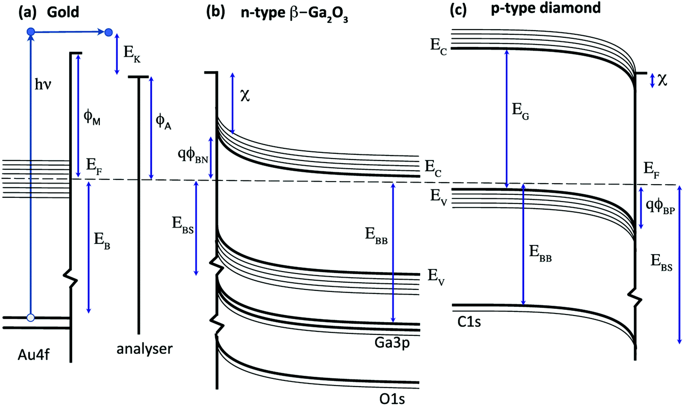 | ||
| Fig. 1 Energy band diagrams for (a) a metal (gold), (b) an n-type semiconductor (β-Ga2O3) and (c) a p-type semiconductor (diamond). The emission process is illustrated for the excitation, emission and collection of a photoelectron from a metal core state in (a). The influence of the potential barriers, ϕBN and ϕBP, on the core level binding energies relative to the Fermi level, EF, are shown in (b) and (c). | ||
For semiconductors, photoelectron spectroscopy can provide direct measurement of key parameters such as the valence and conduction band edges (EV, EC), electron affinity (χ) and interface potential (ϕB) in order to determine the energy band diagrams shown in Fig. 1b and c that are widely used to design and model devices based on semiconductor and metal interfaces.7 In this case, the core level binding energy is not uniquely defined for a given semiconductor since the energy difference between the Fermi level and the band edges depends on the bulk doping level and on the band bending, defined by the potential barrier ϕBN,ϕBP, that results from charges in the depletion region and at the surface.8 This is analogous to the potential energy barrier at a metal–semiconductor or p–n junction and for semiconductor surfaces, correlations can be determined between the energy band diagram shown in Fig. 1 and the surface chemistry, inferred from the line-shape analysis of photoelectron core level spectra.9
For many wide gap semiconductors, doping is a particular challenge and the acceptors or donors may not be fully ionised at room temperature. This results in a high resistivity that can lead to a photovoltage or photocurrent induced charging.10 The Fermi level at the surface does not then align with the analyser, with the charging offset, Eq, affecting the measured kinetic energy as shown in eqn (2).
| EK = hν − EBS − ϕA ± Eq | (2) |
| EBS = EBB ± (qϕB − ζ) | (3) |
| EBS = EBB − (qϕBN − EC + EF) | (4) |
| EBS = EBB + (qϕBP − EF + EV) | (5) |
| EK = hν − EBB ± (qϕB − ζ) − ϕA ± Eq | (6) |
However, for wide-gap semiconductors such as diamond, these binding energies are often larger than kT (the B acceptor is around 15 × kT and the P donor is around 25 × kT at room temperature). This makes doping difficult and increases the room temperature resistivity, introducing a further energy term, Eq, due to surface charging and photovoltage generation during exposure to X-rays.11
For semiconductors, therefore, the core level binding energy depends on a number of factors that must be identified and quantified and these cannot always be uniquely defined in a single XPS measurement. Errors can accumulate within the many terms and any spatial inhomogeneity in the chemical and electronic environment within the measurement volume can also change the lineshape through increased broadening or additional components.12
To complete the electron energy landscape for a semiconductor interface, measurement of the valence band maximum, EV, is needed to determine the band-bending and potential barrier, ϕB. For soft X-ray excitation, core and valence photoelectron spectra can be measured at the same photon energy;13 for laboratory X-ray sources such as Mg and Al Kα, the usual approach is to record the valence band spectra using UV excitation such as He I. These measurements can also provide the metal work function, ϕM, and the semiconductor electron affinity, χ.14 The conduction band maximum, EC, requires a value for the energy band gap, EG, for example from optical measurements, and ζ is calculated from the doping concentration and acceptor (donor) binding energy.15
The surface band bending for both Ga2O3 and diamond has been widely studied and has been reported to be sensitive to the surface composition. In both cases, the Fermi level at the bare surface is pinned within a range that is consistent with the barrier heights measured for metal contacts and that are clustered around the charge neutrality level that lies in the upper half of the energy band gap for Ga2O3 and the lower half of the energy band gap for diamond. This results in similar potential barriers of 1–2 V for both semiconductors that have similar room-temperature band gaps of 4.7 eV (Ga2O3) and 5.6 eV (diamond), as shown in Fig. 1.
XPS studies of semiconductor surfaces can therefore in principle provide a correlation between the energy band profile and changes in the surface chemical environment induced, for example, by adsorption, heating and irradiation.16–18 However, additional measurements are required to identify the influence of sample inhomogeneity and the influence of the measurement method such as final state effects, radiation damage and surface charging.19,20
Here we show how different mechanisms are responsible for the observed core level binding energy changes for a metal alloy and two wide-gap semiconductors when the temperature is cycled between room temperature and 600 °C. Using real-time and near-ambient pressure XPS, where temperature and pressure are the only variables, the dominant physical and chemical effects are identified and corrected.
2 Experimental
2.1 Materials
A gold–silver–copper alloy was prepared by the Diamond Centre Wales (DCW Ltd) using injection mold casting with a predicted composition of 75% gold, 15% silver and 10% copper.21 The sample was then ultrasonically cleaned using acetone, isopropyl alcohol and methanol before mounting in the spectrometer.The β-Ga2O3 single crystal used in this study was a Sn-doped (![[2 with combining macron]](https://www.rsc.org/images/entities/char_0032_0304.gif) 01) single crystal wafer grown using the edge-defined film-fed growth method,22 (Tamura Corporation (Japan)). The carrier concentration was measured to be 4.46 × 1018 cm−3, corresponding to a bulk resistivity of 0.020 Ω cm. The band gap of the (01) β-Ga2O3 wafer was measured optically to be 4.71 ± 0.02 eV; Ti/Au contacts were deposited by e-beam evaporation on part of the front and back sides of each sample. The β-Ga2O3 sample (5 × 5 × 0.65 mm3) investigated here was immersed in 1 M of NaOH at 60 °C for 30 minutes, before drying in N2 gas and mounting into the spectrometer.
01) single crystal wafer grown using the edge-defined film-fed growth method,22 (Tamura Corporation (Japan)). The carrier concentration was measured to be 4.46 × 1018 cm−3, corresponding to a bulk resistivity of 0.020 Ω cm. The band gap of the (01) β-Ga2O3 wafer was measured optically to be 4.71 ± 0.02 eV; Ti/Au contacts were deposited by e-beam evaporation on part of the front and back sides of each sample. The β-Ga2O3 sample (5 × 5 × 0.65 mm3) investigated here was immersed in 1 M of NaOH at 60 °C for 30 minutes, before drying in N2 gas and mounting into the spectrometer.
The p-type diamond (001) sample was a CVD-grown, B-doped single crystal, with a boron concentration of around 1015 cm−3 (Element Six Ltd.).23 The diamond (6 × 8 × 1 mm3) was scaife-polished and oxidised using 10 mL of sulphuric acid and 0.5 g potassium nitrate, followed by cleaning in water and organic solvents and drying in N2 gas before mounting in the spectrometer.
2.2 Methods
Ultrahigh vacuum measurements were recorded using a Mg Kα X-ray excitation source, with photoelectrons continuously energy analysed and detected using a Phoibos 100 analyser with a 2d CCD detector. In the spectrometer, UPS measurements using a SPECS UVS 300 He I/He II UV source with photoelectrons are possible with the same analyser, in the same sample position. Real-time monitoring of core level photoelectron spectra during temperature cycling was enabled by operating the multichannel detector in snapshot mode.24 Programmed annealing cycles were set up by varying the power of a graphite–boron nitride heater and monitoring the temperature, pressure and photoelectron spectra. The sample heating is indirect with the metal directly connected to an external earth to avoid the influence of the bias applied to the heater. A typical cycle between room temperature and 600 °C for the metal alloy required a total time of 5 hours to sequentially record Au4f, Ag3d, and Cu2p snapshot spectra every 20 s, each with a 6 s dwell time. The annealing cycles for the semiconductor samples over the same temperature range involved the collection of Ga2p, Ga3p and O1s core level snapshot spectra for the β-Ga2O3 and the C1s and O1s core level snapshot spectra for the diamond. Near-ambient pressure XPS was carried out at beamline B07-C at Diamond Light Source (DLS) with photoelectrons excited by photons of energy 400 eV to 840 eV and collected in a Phoibos 150 NAP analyser, equipped with a delay line detector operating in scanning (fixed transmission) mode, at pressures from UHV to 10 mbar of oxygen. O1s and C1s core level spectra for the diamond at near-ambient pressures were recorded with higher surface sensitivity at selected temperatures between room temperature and 400 °C at an oxygen pressure of 1 mbar.253 Results and discussion
3.1 Gold alloy
Inert transition metals such as gold, copper and silver provide useful reference samples for XPS measurements. A clean surface can be prepared in situ that is representative of the bulk and the photoelectron spectra measured with typical X-ray excitation have narrow emission peaks covering the full range of kinetic energy. This enables the calibration of the electron analyser to provide reliable reference energy scales for the measurement of binding energy shifts in metal alloys and in non-metals such as semiconductors. A reference metal sample is also useful to identify non-equilibrium charging effects in high resistance materials.Detailed core level emission spectra were recorded with high energy and temporal resolution using multichannel electron detection as shown in Fig. 2a. The Au4f doublet in a Au–Ag–Cu alloy was measured in snapshot mode during a programmed temperature cycle between room temperature (20 °C) and 600 °C. Temperature series for metal alloys are useful to directly monitor effects such as surface desorption and changes in alloy composition. Within each series, the metal core level spectra were fitted using asymmetric pseudo-Voigt functions with fixed Gaussian and Lorentzian mixing ratio and width of 0.7 and 0.4 eV respectively. The variation of peak position with temperature extracted from the fitting sequence for a typical series is shown in Fig. 2b.
 | ||
| Fig. 2 (a) Real-time photoelectron spectroscopy for the 4f core level in a Au–Ag–Cu alloy recorded in snapshot mode during an annealing cycle from room temperature to 600 °C. (b) Curve fitting reveals a reversible kinetic energy shift of +60 meV of the Au4f5/2 photoelectrons as the alloy is heated. | ||
There is an initial increase in peak intensity due to the desorption of surface species with no re-adsorption during cooling. The lineshape is unchanged other than a small increase in broadening which suggests that the surface gold environment is not significantly changed. However, there is a reversible shift in kinetic energy for the fitted Au4f5/2 component as shown in Fig. 2b. This change in energy is observed for each core level and is interpreted as due to the thermal expansion of the alloy. Metals such as gold are expected to have an increase in binding energy when heated, while alkali metals have a decrease in binding energy.26–29 The gold alloy in this case has a rate of change of 0.1 meV K−1 that compares with measurements for elemental gold and suggests a uniform expansion without a significant structural phase change. Relative changes in the peak intensities for the Au, Ag and Cu reflect the alloy composition to reveal stoichiometric changes at the surface as the temperature is increased. The energy shift is reliably measured in real-time with a fixed geometry by minimising experimental uncertainty due to changes in sample position. Calibration of the energy scale using pure metals reveal that the initial binding energy of the Au4f core levels for this alloy differ by less than 0.1 eV from the reference gold spectra due to a charge transfer effect in the alloy.30 Changes in surface alloy composition with temperature has relevance for soldering application in sectors such as jewellery and dentistry, where the joints become fail points.31,32 These studies enable metal migration of elements such Cu and Ag to be followed in real time, to better mitigate risks.33
3.2 n-type β-Ga2O3
The temperature sequence for the Ga2p3/2 core level photoelectron spectrum for β-Ga2O3 is shown in Fig. 3a. Also recorded in the sequence were the Ga3p3/2 and O1s photoelectron emission spectra. The initial increase in intensity is due to the desorption of weakly-adsorbed species and is reflected in an increase in the corresponding O1s photoelectron emission and a decrease in the C1s photoelectron emission. The Ga and O core level emission spectra for the initial surface were fitted with two components and no additional components were required to fit the sequence shown in Fig. 3a. The components are broad such that identification of all surface species requires a higher surface sensitivity than available using these laboratory sources. For example, it has been shown using synchrotron radiation excitation that different adsorption sites are possible for surface OH species and that these are sensitive to the surface treatment.34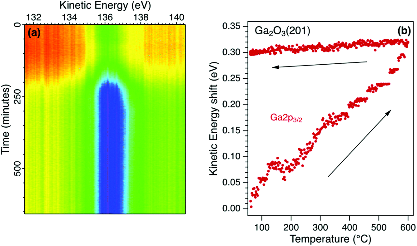 | ||
| Fig. 3 (a) Real-time photoelectron spectroscopy for an n-type β-Ga2O3 single crystal during an annealing cycle from room temperature to 600 °C. The Ga2p3/2 core level increases in intensity up to 600 °C and shows a significant, irreversible energy shift of 300 meV to higher kinetic energy (b). | ||
The peak position for the Ga2p3/2 core level, extracted from the real-time sequence is shown in Fig. 3b. There is a significant increase in kinetic energy (decrease in binding energy) as the temperature is increased to 600 °C that is not reversed when the temperature is decreased to 20 °C. This irreversible shift is interpreted as a change in the potential barrier due to a change in surface states and Fermi level pinning. There is no evidence of surface charging for this semiconductor due to its low potential barrier, high doping concentration and low resistivity. During heating to 600 °C, the relative Ga![[thin space (1/6-em)]](https://www.rsc.org/images/entities/char_2009.gif) :O ratio is increased as the surface OH species are desorbed irreversibly in vacuum. The O1s core level spectrum can be fitted with two components, a larger bulk peak corresponding to oxygen in Ga2O3 and a smaller low binding energy component due to surface OH groups. The latter component is reduced on heating as the OH is desorbed with the total area of the O1s reducing by 3%.35 There is a corresponding change in the Ga core level lineshape as the Ga–OH component is removed on heating. The binding energies of the core levels in this n-type semiconductor are therefore correlated with the surface composition which affects the surface electronic states and hence potential barrier.36 Knowledge of the thermal stability of semiconducting oxides is essential for device applications where the surface termination and band profile change with temperature.37
:O ratio is increased as the surface OH species are desorbed irreversibly in vacuum. The O1s core level spectrum can be fitted with two components, a larger bulk peak corresponding to oxygen in Ga2O3 and a smaller low binding energy component due to surface OH groups. The latter component is reduced on heating as the OH is desorbed with the total area of the O1s reducing by 3%.35 There is a corresponding change in the Ga core level lineshape as the Ga–OH component is removed on heating. The binding energies of the core levels in this n-type semiconductor are therefore correlated with the surface composition which affects the surface electronic states and hence potential barrier.36 Knowledge of the thermal stability of semiconducting oxides is essential for device applications where the surface termination and band profile change with temperature.37
3.3 p-type diamond
The room temperature diamond photoelectron spectrum is dominated by emission from the C1s core level with a small emission from the O1s core level corresponding to a monolayer coverage (1 mL). The initial annealing of this surface in ultrahigh vacuum (UHV) to 400 °C desorbs residual surface contaminants, resulting in a small increase in core level emission and this is evident in the sequence of C1s snapshot spectra for the oxidised diamond (001) surface in Fig. 4a. This surface is stable when the maximum annealing temperature is below 400 °C, with both C1s and O1s core level emission spectra showing a reversible change in kinetic energy without change in lineshape. This reversible change is sensitive to the X-ray flux and is interpreted as a room temperature photovoltage, as reported for a H-terminated diamond (111) crystal with a similar boron concentration measured in the same environment.38 For the (111) diamond, the observed shift and its saturation at higher temperature was modelled using the diamond resistivity as the main temperature-dependent variable. At room temperature, the photoexcitation process generates electrons and holes in the depletion region that are separated, with electrons accumulating at the surface when the resistance to earth in the diamond is high. Under these conditions, the surface is at a negative potential relative to the electron analyser and this leads to an increase in the measured electron binding energy and a decrease in the kinetic energy. As the temperature is increased, the diamond resistance and the depletion width decrease and the surface photovoltage reduces to zero. At room temperature, the bulk diamond peak for the p-type diamond (001) (Fig. 4a) was found to have an apparent binding energy similar to graphite rather than its true value of 285.4 eV that is only revealed at the higher temperature.38,39 This surface photovoltage was also observed for this diamond when irradiated with He I and synchrotron radiation at room temperature and was found to persist when measured at near-ambient pressure of oxygen. Ultraviolet Photoelectron Spectroscopy (UPS) measurements for this moderately-B-doped diamond at the higher temperature yield a barrier height that is close to that predicted by the charge neutrality level but is dependent on the surface preparation.40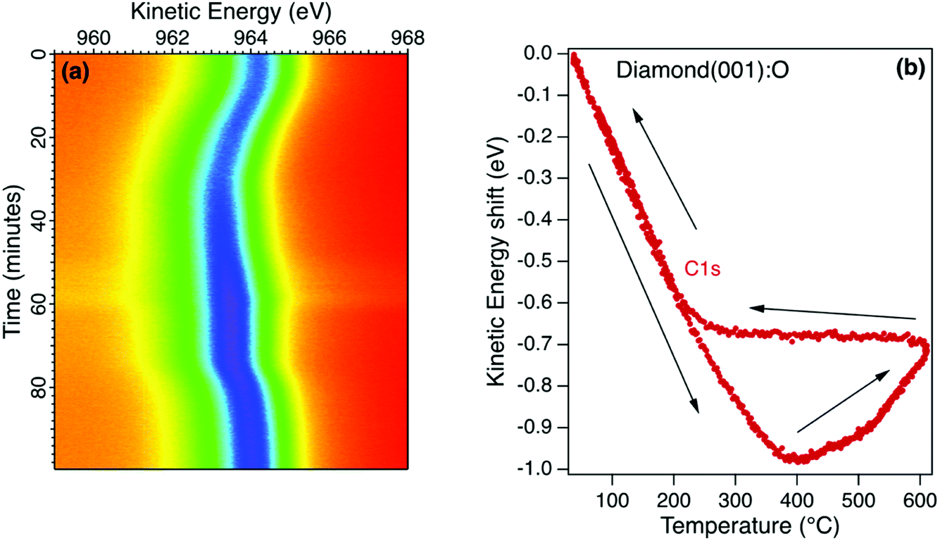 | ||
| Fig. 4 (a) Real-time photoelectron spectroscopy for a p-type diamond single crystal during an annealing cycle from room temperature to 600 °C. (b) The kinetic energy of the dominant component of the C1s core level emission spectrum exhibits a reversible decrease of 960 meV on heating to 400 °C due to the removal of a surface photovoltage. Between 400 °C and 600 °C the energy shift is reversed and is unchanged on cooling to 200 °C. A surface photovoltage returns on cooling to room temperature. | ||
Above 400 °C there is a loss of surface oxygen and a reversal of the peak shift as shown in Fig. 4b for the sequence of C1s snapshot spectra recorded during a temperature cycle between room temperature and 600 °C. During the cooling phase, the peak position remained constant between 600 °C and 200 °C, returning to an energy close to the starting value at room temperature. The irreversible shift at higher temperatures is similar to that observed for the Ga oxide, corresponding to a decrease in the potential barrier for the p-type diamond as the surface oxygen is desorbed. Below 200 °C therefore, the surface photovoltage dominates and for this moderately-doped diamond, the true potential barrier is only correctly measured at the higher temperature when the resistance is sufficiently low to ensure equilibrium.
To separate the influence of surface photovoltage from chemical changes, the annealing of the oxygen-terminated diamond (001) surface was repeated under 1 mbar of molecular oxygen as shown in Fig. 5. The C1s spectrum (Fig. 5a) is dominated by a main peak at a binding energy of 284.6 eV at 55 °C corresponding to C–C bonding in the bulk diamond, with a broad, multi-component shoulder at higher binding energy associated with C atoms in different C–O bonding environments. Non-diamond carbon contamination was minimal on this surface as there is a negligible component at low binding energy. The thermal annealing cycle resulted in small line shape changes but the main observation in Fig. 5a is a rigid energy shift that affects all peaks and components as observed in UHV. The O1s spectrum (Fig. 5b) is dominated by an ether (C–O–C) component at a binding energy of 531.9 eV at 55 °C, with lower intensity components due to other species such as ketones at lower binding energies.41 The doublet at 537.3 eV and 538.4 eV corresponds to photoelectron emission from molecular oxygen in the gas phase above the surface.42,43 The O1s emission peak for the oxidised diamond surface at the lower temperatures (Fig. 5b) has a similar lineshape when measured at UHV and in 1 mbar of oxygen confirming that the surface remained oxidised during the 400 °C annealing cycle in oxygen. At 400 °C, the substrate and gas phase peaks are shifted to higher binding energy, with a similar shift for the C1s core level. This energy shift in both core levels is dependent on temperature as shown in Fig. 5c and seems to be insensitive to the pressure. The reversible energy shift in the photoelectron spectra is similar to that observed in UHV and in this case can only be associated with physical effects. This surface processing method of annealing in oxygen has been shown to provide the optimal surface for diamond quantum technology applications.44
 | ||
| Fig. 5 Near-ambient pressure photoelectron emission spectra for the C1s (a) and O1s (b) core level in a p-type diamond (001) single crystal measured at 55 °C and 400 °C in 1 mbar of O2 and at 20 °C in UHV. The incident photon energy for the synchrotron radiation excitation source was 840 eV in both cases. The kinetic energy of all peaks (c) changes with temperature during annealing in UHV and in 1 mbar of O2 with a reversible shift as observed for higher energy X-ray excitation in UHV (Fig. 4). | ||
Correction for the surface photovoltage effect in diamond and confirmation of equilibrium measurement of β-Ga2O3 enables a direct comparison of the energy band diagrams for the two wide-gap semiconductors as shown in Fig. 6. In both cases, there are several possible adsorption sites and oxygen-containing species which have different photoelectron binding energies, making their precise identification difficult, especially in laboratory XPS measurements. The density of electronic states that determine the surface Fermi level pinning is below the sensitivity of the measurements and cannot be directly measured in general. However, the parallel monitoring of photoelectron spectra during temperature annealing can reveal these correlations indirectly as demonstrated for these two wide-gap semiconductors. In Fig. 6a, only one possible OH site, bonded to surface Ga atoms, is shown to illustrate the desorption that is observed during heating to 600 °C. During this processing, the potential barrier for this n-type semiconductor increases from ϕBN1 to ϕBN2 as shown in Fig. 6b. For β-Ga2O3, therefore, the electronic properties are strongly dependent on adsorbed OH species, with the upward band bending increased irreversibly for the NaOH-treated surface when OH species are desorbed. For p-type diamond, the oxidised (001) surface is dominated by bridge C–O–C bonding, although other bonding configurations such as C–OH, C–H and C![[double bond, length as m-dash]](https://www.rsc.org/images/entities/char_e001.gif) O are usually present. This is shown schematically in Fig. 6c, with oxygen desorption above 400 °C prevented by measurement at a pressure of 1 mbar of molecular oxygen. Under these conditions, the core level binding energy is reversible, and the band bending is determined by a surface photovoltage, VSPV, and the potential barrier ϕBN is unchanged as shown in Fig. 6d. The true barrier height is close to that measured for most metal contacts17 that suggests a Fermi level pinning close to the charge neutrality level. Above 400 °C, surface oxygen is desorbed in vacuum and this reduces the downward band bending on this p-type diamond surface. The potential barriers for both n-type β-Ga2O3 and p-type diamond are thus sensitive to surface oxygen composition.
O are usually present. This is shown schematically in Fig. 6c, with oxygen desorption above 400 °C prevented by measurement at a pressure of 1 mbar of molecular oxygen. Under these conditions, the core level binding energy is reversible, and the band bending is determined by a surface photovoltage, VSPV, and the potential barrier ϕBN is unchanged as shown in Fig. 6d. The true barrier height is close to that measured for most metal contacts17 that suggests a Fermi level pinning close to the charge neutrality level. Above 400 °C, surface oxygen is desorbed in vacuum and this reduces the downward band bending on this p-type diamond surface. The potential barriers for both n-type β-Ga2O3 and p-type diamond are thus sensitive to surface oxygen composition.
 | ||
| Fig. 6 (a) Schematic diagram of the β-Ga2O3 (01) surface with calculated atomic co-ordinates from Anvari et al.35 The surface is terminated by OH groups that are desorbed during heating from room temperature to 600 °C. This affects the band bending as shown in (b). (c) The oxygen-terminated diamond (001) surface with calculated atomic co-ordinates from ref. 44 and 45 is preserved by heating to 400 °C in 1 mbar O2. The apparent change in core level binding energy at high temperature is due to the removal of a surface photovoltage with an unchanged potential barrier as shown in (d). | ||
4 Conclusions
Real-time measurements reveal shifts in measured kinetic energy for all three samples, but the origin in each case is different. For the metal alloy, the binding energy shift of 60 meV is reversible and is due to thermal expansion. For the n-type β-Ga2O3, the shift of 300 meV to lower binding energy is due to a change in surface state pinning of the Fermi level as surface OH species are desorbed. For the p-type diamond, there is a reversible shift at temperatures below 400 °C due to the removal of a surface photovoltage and an irreversible shift above 400 °C, due to a change in surface Fermi level pinning position as the surface oxygen is desorbed. When the oxygen is replenished by heating in an oxygen environment, the shift is fully reversible. Corrected binding energy values aid the completion of the energy band diagrams for these wide-gap semiconductors and provide protocols for surface processing to engineer key surface and interface parameters.Author contributions
SA, DH, KH, JA, RC, SC, MA, GW and AE contributed to the research and investigation using experimental measurements at Aberystwyth. SA, KH, JA, RC, SC, FV, GH, DG, PF, RA and AE contributed to the research and investigation using synchrotron radiation at the Diamond Light Source. JE and KJ provided and prepared the metal alloy materials. All authors contributed to the analysis and interpretation of measurements and to the final manuscript.Conflicts of interest
There are no conflicts to declare.Acknowledgements
The authors acknowledge the financial support of the EPSRC CDT in Diamond Science and Technology, the Diamond Light Source (instrument B07-C/VerSoX; proposal SI18182), the European Regional Development Fund through the Solar Photovoltaic Academic Research Consortium (SPARC II) and the Centre for Photonics Expertise (CPE) operated by the Welsh Government. We thank R. F. Martinez-Gazoni and R. J. Reeves of the School of Physical and Chemical Sciences, University of Canterbury, New Zealand, for their help in the preparation and characterisation of the β-Ga2O3 samples.References
- M. P. Seah, I. S. Gilmore and S. J. Spencer, J. Electron Spectrosc. Relat. Phenom., 2001, 120, 93–111 CrossRef CAS.
- J. C. Fuggle and S. F. Alvardo, Phys. Rev. A: At., Mol., Opt. Phys., 1980, 22, 1615–1624 CrossRef CAS.
- M. Descostes, F. Mercier, N. Thromat, C. Beaucaire and M. Gautier-Soyer, Appl. Surf. Sci., 2000, 165, 288–302 CrossRef CAS.
- K. J. Kim, D. W. Moon, C. J. Park, D. Simons, G. Gillen, H. Jin and H. J. Kang, Surf. Interface Anal., 2007, 39, 665–673 CrossRef CAS.
- J. M. Cerrato, M. F. Hochella, W. R. Knocke, A. M. Dietrich and T. F. Cromer, Environ. Sci. Technol., 2010, 44, 5881–5886 CrossRef CAS PubMed.
- J. Yan, A. D. Carl, A. R. Maag, J. C. Macdonald, P. Müller, R. L. Grimm and S. C. Burdette, Dalton Trans., 2019, 48, 4520–4529 RSC.
- W. Mönch, Rep. Prog. Phys., 1990, 53, 221–278 CrossRef.
- T. Veal, P. Jefferson, L. Piper, C. F. McConville, T. Joyce, P. Chalker, L. Considine, H. Lu and W. Schaff, Appl. Phys. Lett., 2006, 89, 202110 CrossRef.
- D. Caliskan, H. Sezen, E. Ozbay and S. Suzer, Sci. Rep., 2015, 5, 14091 CrossRef PubMed.
- D. R. Baer, K. Artyushkova, H. Cohen, C. D. Easton, M. Engelhard, T. R. Gengenbach, G. Greczynski, P. Mack, D. J. Morgan and A. Roberts, J. Vac. Sci. Technol., A, 2020, 38, 031204 CrossRef CAS.
- J. Y. Tsao, et al. , Adv. Electron. Mater., 2018, 4, 1600501 CrossRef.
- C. J. Powell and M. P. Seah, J. Vac. Sci. Technol., A, 1990, 8, 735–763 CrossRef CAS.
- G. A. Rooke, J. Res. Natl. Bur. Stand., Sect. A, 1970, 74, 273–279 CrossRef CAS PubMed.
- L. Diederich, O. M. Küttel, P. Aebi and L. Schlapbach, Surf. Sci., 1998, 418, 219–239 CrossRef CAS.
- S. Rafique, L. Han, S. Mou and H. Zhao, Opt. Mater. Express, 2017, 7, 3561–3570 CrossRef CAS.
- S. Santucci, C. Cantalini, M. Crivellari, L. Lozzi, L. Ottaviano and M. Passacantando, J. Vac. Sci. Technol., A, 2000, 18, 1077 CrossRef CAS.
- D. A. Evans, H. J. Steiner, S. Evans, R. Middleton, T. S. Jones, S. Park, T. U. Kampen, D. R. T. Zahn, G. Cabailh and I. T. McGovern, J. Phys.: Condens. Matter, 2003, 15, S2729 CrossRef CAS.
- J. Wu, B. Wang, F. Yi, S. Deng, N. Xu and J. Chen, RSC Adv., 2018, 8, 752–760 RSC.
- F. S. Roberts, S. L. Anderson, A. C. Reber and S. N. Khanna, J. Phys. Chem. C, 2015, 119, 6033–6046 CrossRef CAS.
- M. Bär, J.-P. Theisen, R. G. Wilks, F. Erfurth, R. Félix, D. Gerlach, S. Haas, L. Tati Bismaths, F. Reinert, F. Kronast, T. P. Niesen, J. Palm, S. Visbeck and L. Weinhardt, J. Appl. Phys., 2013, 113, 193709 CrossRef.
- B. Henriques, P. Pinto, J. Souza, J. C. Teixeria, D. Soares and F. S. Silva, Gold Bull., 2013, 46, 117–225 CrossRef CAS.
- A. Kuramata, K. Koshi, S. Watanabe, Y. Yamaoka, T. Masui and S. Yamakoshi, Jpn. J. Appl. Phys., 2016, 55, 1202A2 CrossRef.
- T. Kwak, J. Lee, G. Yoo, H. Shin, U. Choi, B. So, S. Kim and O. Nam, Phys. Status Solidi A, 2020, 217, 1900973 CrossRef CAS.
- T. R. Chase, D. A. Evans, D. P. Langstaff and A. Bushell, Nucl. Instrum. Methods Phys. Res., Sect. B, 2005, 238, 219–223 CrossRef.
- G. Held, F. Venturini, D. Grinter, P. Ferrer, R. Arrigo, L. Deacon, W. Quevedo Garzon, K. Roy, A. Large, C. Stephens, A. Watts, P. Larkin, M. Hand, H. Wang, L. Pratt, J. J. Mudd, T. Richardson, S. Patel, M. Hillman and S. Scott, J. Synchrotron Radiat., 2020, 27, 1153–1166 CrossRef CAS PubMed.
- D. M. Riffe, G. K. Wertheim, D. N. Buchanan and P. H. Citrin, Phys. Rev. B: Condens. Matter Mater. Phys., 1992, 45, 6216–6225 CrossRef CAS PubMed.
- D. M. Riffe, W. Hale, B. Kim and J. L. Erskine, Phys. Rev. B: Condens. Matter Mater. Phys., 1996, 54, 17118–17122 CrossRef CAS PubMed.
- T. Durakiweicz, J. A. J. Arko, J. J. Joyce, D. J. P. Moore and A. S. Halas, Surf. Sci., 2001, 478, 72–82 CrossRef.
- K. Shen, G. Li and W. Wang, Trans. Nonferrous Met. Soc. China, 2016, 26, 2900–2909 CrossRef CAS.
- D. Wang, X. Cui, Q. Xiao, Y. Hu, Z. Wang, Y. M. Yiu and T. K. Sham, AIP Adv., 2018, 8, 065210 CrossRef.
- I. Watanabe, E. Watanabe, M. Atsuta and T. Okabe, J. Prosthet. Dent., 1997, 78, 260–266 CrossRef CAS.
- R. Süss, E. van der Lingen, L. Glaner and M. du Toit, Gold Bull., 2004, 37, 196–207 CrossRef.
- F. W. Jones and C. Sykes, Proc. R. Soc. London, Ser. A, 1938, 166, 376–390 CAS.
- R. M. Gazoni, L. Caroll, J. I. Scott, S. Astley, D. A. Evans, A. J. Downard, R. J. Reeves and M. W. Allen, Phys. Rev. B, 2020, 102, 035304 CrossRef CAS.
- R. Anvari, D. Spagnoli, G. Parish and B. Nener, Chem.–Eur. J., 2018, 24, 7445–7455 CrossRef CAS PubMed.
- J. E. N. Swallow, J. B. Varley, L. A. H. Jones, J. T. Gibbon, L. F. J. Piper, V. R. Dhanak and T. D. Veal, APL Mater., 2019, 7, 022528 CrossRef.
- R. Heinhold, S. P. Cooil, D. A. Evans and M. W. Allen, J. Phys. Chem. C, 2014, 118, 24575–24582 CrossRef CAS.
- G. T. Williams, S. P. Cooil, O. R. Roberts, S. Evans, D. P. Langstaff and D. A. Evans, Appl. Phys. Lett., 2014, 105, 061602 CrossRef.
- S. J. Schmeig and D. N. Belton, Surf. Sci. Spectra, 1992, 1, 333 CrossRef.
- S. J. Sque, R. Jones and P. R. Briddon, Phys. Rev. B: Condens. Matter Mater. Phys., 2006, 73, 085313 CrossRef.
- F. Maier, J. Ristein and L. Ley, Phys. Rev. B: Condens. Matter Mater. Phys., 2001, 64, 165411 CrossRef.
- J. Schnadt, J. Knudsen, J. N. Andersen, H. Siegbahn, A. Pietzsch, F. Hennies, N. Johansson, N. Mårtensson, G. Öhrwall, S. Bahr, S. Mähld and O. Schaff, J. Synchrotron Radiat., 2012, 19, 701–704 CrossRef CAS PubMed.
- P. E. Pehrsson and T. W. Mercher, Surf. Sci., 2000, 460, 59–66 Search PubMed.
- S. Sangtawesin, B. L. Dwyer, S. Srinivasan, J. J. Allred, L. V. H. Rodgers, K. De Greve, A. Stacey, N. Dontschuk, K. M. O’Donnell, D. Hu, D. A. Evans, C. Jaye, D. A. Fischer, M. L. Markham, D. J. Twitchen, H. Park, M. D. Lukin and N. P. de Leon, Phys. Rev. X, 2019, 9, 03105 Search PubMed.
- D. Petrini and K. Larsson, J. Phys. Chem., 2007, 111, 795–801 CAS.
| This journal is © The Royal Society of Chemistry 2022 |