 Open Access Article
 This Open Access Article is licensed under a
 Creative Commons Attribution 3.0 Unported Licence
Oxygen relocation during HfO2 ALD on InAs
Giulio
D’Acunto
 ab,
Esko
Kokkonen
c,
Payam
Shayesteh
ab,
Virginia
Boix
ab,
Foqia
Rehman
ab,
Zohreh
Mosahebfard
abe,
Erik
Lind
bd,
Joachim
Schnadt
abc and
Rainer
Timm
*ab
ab,
Esko
Kokkonen
c,
Payam
Shayesteh
ab,
Virginia
Boix
ab,
Foqia
Rehman
ab,
Zohreh
Mosahebfard
abe,
Erik
Lind
bd,
Joachim
Schnadt
abc and
Rainer
Timm
*ab
aDivision of Synchrotron Radiation Research, Department of Physics, Lund University, 22100 Lund, Sweden. E-mail: Rainer.Timm@sljus.lu.se
bNanoLund Center for Nanoscience, Lund University, 22100 Lund, Sweden
cMAX IV Laboratory, Lund University, 22100 Lund, Sweden
dDepartment of Electrical and Information Technology, Lund University, 22100 Lund, Sweden
eDepartment of Physics, University of Siegen, 57072 Siegen, Germany
First published on 20th January 2022
Abstract
Atomic layer deposition (ALD) is one of the backbones for today’s electronic device fabrication. A critical property of ALD is the layer-by-layer growth, which gives rise to the atomic-scale accuracy. However, the growth rate – or growth per cycle – can differ significantly depending on the type of system, molecules used, and several other experimental parameters. Typically, ALD growth rates are constant in subsequent ALD cycles, making ALD an outstanding deposition technique. However, contrary to this steady-state – when the ALD process can be entirely decoupled from the substrate on which the material is grown – the deposition’s early stage does not appear to follow the same kinetics, chemistry, and growth rate. Instead, it is to a large extent determined by the surface composition of the substrate. Here, we present evidence of oxygen relocation from the substrate-based oxide, either the thermal or native oxide of InAs, to the overlayer of HfO2 in the initial ALD phase. This phenomenon enables control of the thickness of the initial ALD layer by controlling the surface conditions of the substrate prior to ALD. On the other hand, we observe a complete removal of the native oxide from InAs already during the first ALD half-cycle, even if the thickness of the oxide layer exceeds one monolayer, together with a self-limiting thickness of the ALD layer of a maximum of one monolayer of HfO2. These observations not only highlight several limitations of the widely used ligand exchange model, but they also give promise for a better control of the industrially important self-cleaning effect of III–V semiconductors, which is crucial for future generation high-speed MOS.
Introduction
The future development of semiconductor technology is intimately connected to the development of faster and smaller devices, with a reduced power consumption. The research efforts towards this goal are intensive, not least in relationship to the metal oxide semiconductor field-effect transistor (MOSFET). One of the most significant limitations of present MOSFET technology is the use of silicon, which, although cheap and easy to produce, can hardly reach the required speed of device operation needed to achieve the development goals defined by the International Technology Roadmap for Semiconductors.1 A first step towards the replacement of Si materials has been made by replacing the native silicon oxide with a high-κ oxide such as HfO2, allowing drastically smaller gate sizes.2–4 Substituting the silicon channel material with a III–V semiconductor has often been suggested as another promising step towards faster MOSFET devices.2,5 Among the III–V semiconductors, InAs plays a particularly important role, since it has a narrow band gap compared to that of silicon and an electron mobility that is around 20 times higher than that of silicon;6 these properties make InAs particularly suitable for use in new-generation high-speed metal oxide semiconductor transistors, especially in radio frequency applications.2,3,7One of the challenges that must be overcome before InAs/HfO2 MOSFET devices can enter a broad market is to obtain a clean interface between the two materials. The quality of this interface plays an essential role, since defects related to the oxide of the substrate InAs hinder the overall device performance. Atomic layer deposition (ALD) is a deposition technique that potentially can provide a defect-free and conformal layer of HfO2 over the entire surface of InAs; especially as it comes along with the so-called “self-cleaning” effect, which comprises the removal of the unwanted native oxide from InAs together with the deposition of the desired HfO2. This “self-cleaning” or “clean-up” effect has been reported for native oxides of typical III–V surfaces including InAs, GaAs, GaSb, and mixed alloys of these materials8–13 upon the ALD of Al2O3 and HfO2, performed with trimethylaluminum (TMA) and tetrakis(DMA−)hafnium (TDMAHf, where DMA− stands for the dimethylamido ligands), respectively. However, many questions about the efficiency of the self-cleaning and the surface chemical reactions during the ALD process behind this are still unsolved, leaving substantial room for improvement of the resulting III–V/high-κ interface.
ALD, with enormous potential in a large variety of material-dependent technologies,14–17 is based on the self-limiting reaction of gaseous precursors with the surface of a substrate. The ALD of transition metal oxides, such as HfO2, uses two precursors, a metal and an oxygen one. After one cycle of ALD, defined by self-limiting reactions of the two precursors with the surface in two separate half-cycles, ideally one monolayer of the chosen material is obtained. The self-limiting deposition step, which is the basis of the layer-by-layer growth in ALD and which ensures control and uniformity of the ALD layers, is often described by an ideal reaction mechanism. In reality, typically more or less severe deviations from the ideal mechanism occur.18,19 For example, the standard model of the ALD of high-κ oxide is based on a ligand exchange reaction mechanism, which does not consider the surface as an active element. This assumption is in contrast to the experimentally observed and strongly appreciated self-cleaning effect.
One should expect the influence of the substrate to decrease with an increasing number of ALD cycles. This is also reflected by the thickness of the ALD layer which, according to the ideal ALD mechanism, should grow linearly with increasing numbers of ALD cycles. Numerous studies already show that this linearity only exists from a certain number of cycles onward, while the initial ALD cycles behave differently and can be characterized by either higher or lower growth rates. For more details, we suggest the review by Sønsteby et al.20 The number of cycles after which the overlayer growth is completely decoupled from the surface can vary strongly, depending on experimental parameters and especially the precursor pulse length. Importantly, the surface chemistry that defines the final interface between the substrate and the ALD-grown overlayer typically occurs during the initial half-cycles of ALD,8,12,13i.e. before the decoupling and, thus, before the ideal ALD models gain validity. Hence, it is important to obtain better insight into the details of the initial ALD process, where the influence of the surface plays a significant role.
Here, we investigate eight InAs samples prepared with varying oxide thicknesses, ranging from a few Å to a few nanometres, by ambient pressure X-ray photoelectron spectroscopy (AP-XPS), a method which allows the real-time monitoring of the deposition process.8,21,22 We evaluate the influence of the surface on the composition and thickness of the overlayer of HfO2 already formed during the first half cycle of ALD performed with TDMAHf. We find evidence that the interaction with the TDMAHf molecules guarantees perfect self-cleaning, i.e. the removal of almost all InAs oxide irrespective of the initial oxide thickness. The interface is sharp and defect-free and characterized by the presence of a thin In–O–Hf layer. The oxygen contained in the original InAs oxide is used to form HfO2 already in the first ALD half-cycle. We find that the thickness of the thus formed HfO2 layer appears to be self-limited to one monolayer. Interestingly, we also find that TDMAHf does not interact with the clean InAs surface, but only with its oxide.
The results show that the ligand exchange model becomes valid only after the initial ALD half-cycle, and they provide answers to previously open questions about the role of oxygen atoms during the self-cleaning effect. Furthermore, the observation of a sharp, defect-free InAs/high-κ interface is of high relevance for future MOSFET applications. Our findings suggest that the quality of the interface will depend strongly on the ALD parameters, especially a sufficiently long first half cycle, rather than the exact thickness and chemical composition of the initial InAs oxide.
Experimental
The experiments were performed at the AP-XPS end stations of the SPECIES beamline23 of the MAX IV Laboratory in Lund, Sweden, and of the I511/SPECIES beamlines at the previous MAX-lab24–26 synchrotron radiation facility. Eight samples of InAs were treated equally in the cleaning process as follows (cf.Table 1): the samples were etched in 37% HCl![[thin space (1/6-em)]](https://www.rsc.org/images/entities/char_2009.gif) :H2O 1:1 for 30 s to remove the original native oxide and other contamination and then rinsed in ultrapure water for 60 s. The result of this first treatment step is a clean InAs (100) surface, which after the water rinse and subsequent contact to air is covered with a thin native oxide again. After that, the samples were mounted onto a stainless-steel sample holder and transferred to the ultrahigh vacuum (UHV) preparation chamber of the beamline. Samples E, F, G and H did not receive any other treatment, while samples A, B, C and D were heated up to around 360 °C and exposed to atomic hydrogen for 20 minutes, obtained using a thermal cracker (from MBE Komponenten) operated at about 1700 °C and a H2 pressure of 2 × 10⁻⁶ mbar. This process produced four clean InAs surfaces without the presence of oxygen or carbon (as inspected by XPS). A more detailed study of the atomic hydrogen cleaning procedure can be found in ref. 27. No other treatment was done for one of the samples (here called sample A). For the other three samples, exposure to oxygen was performed in the preparation chamber at a sample temperature of 320 °C: 0.05 L (sample B), 6 L (sample C) and 10 L (sample D). The cleaning treatments performed on each sample are summarised in Table 1.
:H2O 1:1 for 30 s to remove the original native oxide and other contamination and then rinsed in ultrapure water for 60 s. The result of this first treatment step is a clean InAs (100) surface, which after the water rinse and subsequent contact to air is covered with a thin native oxide again. After that, the samples were mounted onto a stainless-steel sample holder and transferred to the ultrahigh vacuum (UHV) preparation chamber of the beamline. Samples E, F, G and H did not receive any other treatment, while samples A, B, C and D were heated up to around 360 °C and exposed to atomic hydrogen for 20 minutes, obtained using a thermal cracker (from MBE Komponenten) operated at about 1700 °C and a H2 pressure of 2 × 10⁻⁶ mbar. This process produced four clean InAs surfaces without the presence of oxygen or carbon (as inspected by XPS). A more detailed study of the atomic hydrogen cleaning procedure can be found in ref. 27. No other treatment was done for one of the samples (here called sample A). For the other three samples, exposure to oxygen was performed in the preparation chamber at a sample temperature of 320 °C: 0.05 L (sample B), 6 L (sample C) and 10 L (sample D). The cleaning treatments performed on each sample are summarised in Table 1.
| A | B | C | D | E, F, G and H |
|---|---|---|---|---|
| Hydrogen cleaned | Hydrogen cleaned + 0.05 L O2 | Hydrogen cleaned + 6.00 L O2 | Hydrogen cleaned + 10.00 L O2 | Water bath |
The first HfO2 ALD half-cycle on all InAs(100) samples was performed with TDMAHf in the reaction cell of the AP-XPS chamber with the sample heated to 200–220 °C. The TDMAHf container (acquired from Strem Chemicals, Inc.) was attached to the gas system of the setup and heated to about 80 °C in order to increase the vapour pressure. The reaction cell was operated in constant flow mode, so that the TDMAHf was delivered at a constant pressure of about 10−3 mbar, measured by a gauge installed on the outlet of the gas line system. No carrier gases were used.
The InAs surfaces were first characterized in UHV with XPS. Then, time-resolved AP-XPS experiments were performed during the TDMAHf deposition; finally, another characterization data set was measured after the precursor gases were evacuated at a pressure of around 10−6 mbar. The spectra acquired before and after each half cycle were collected at 675 eV and 350 eV photon energy with a total instrumental broadening of around 0.35 eV for samples A, B, C and D. For the other samples (E, F, G and H), photon energies of 300 eV, 330 eV and 900 eV were used for the In 4d/Hf 4f and As 3d core levels and overview spectra, respectively, with a total instrumental broadening of around 0.50 eV. The sequences of In 4d, Hf 4f, and As 3d core-level spectra recorded during TDMAHf exposure at ∼10−3 mbar were measured with a photon energy of 675 eV. The time resolved spectra were measured in the fixed mode of the electron energy analyser in a sequence that took around six seconds to complete. The X-ray photoelectron (XP) spectra were curve-fitted using the IGOR Pro software by Wavemetrics, Inc. The binding energies were calibrated to the As 3d5/2 bulk component set to 41.0 eV.28–31 Shirley backgrounds were removed before the fit. The intensities were normalized to that of the As 3d bulk component.
The thickness evaluation of the thermal oxide was carried out using an overlayer model explained elsewhere.8 The cross sections, inelastic mean free paths, and atom densities were estimated from literature values.8
Results
In this section, we will first present the results on InAs samples covered by a thin thermal oxide layer and then on those with a slightly thicker native oxide layer. Finally, we will discuss the role of the oxide layers during the first half-cycle of ALD. The thermal and native oxides have a similar chemical composition and differ mainly in their thickness. The growth rate and stoichiometry of the thermal oxides can be controlled rather well, which is not the case for the native oxides. Moreover, as previously shown by our group,21 the interface between the InAs surface and the high-κ oxide deposited by ALD is improved in terms of the interfacial defect densities, Fermi level unpinning and lower capacitance frequency dispersion when the ALD is carried out on an InAs surface covered by a thermal oxide layer in comparison to a native oxide-covered surface. In the present experiment, we have investigated both types of oxide for a practical reason: growing a thick thermal oxide layer is difficult, as is achieving thin native oxide layers. Since the goal of the current experiment is to compare thin and thick oxide layers, we adopt thermal oxidation of InAs to achieve submonolayer oxides and native oxidation to achieve thick oxide layers.Thermal and native oxides of InAs, before TDMAHf deposition
We start by describing the state of the InAs surface and the effect of the treatments on the composition and thickness of the grown oxide layer. The surfaces do not exhibit any considerable C or N contamination, as can be seen from the survey spectra of samples A, C and G, shown in Fig. 1. High-resolution spectra of the As 3d and In 4d core levels before TDMAHf deposition are reported in Fig. 2. The As 3d XP spectrum of sample A, acquired at a photon energy of 350 eV, is shown in Fig. 2a. The As 3d spectrum is characterized by a doublet centred at 41.0 eV, and no component due to As oxide is visible. The corresponding In 4d core level (cf.Fig. 2b), measured at a photon energy of 350 eV, is characterized by a dominant doublet at 17.6 eV, corresponding to In bonded to As, and a small shoulder towards high binding energy associated with In oxide (found at 18.1 eV; +0.5 eV from the bulk component); these values are in line with values found elsewhere in the literature.8,12,32 The hydrogen cleaning process should result in an InAs surface without any oxide;21 however, clearly this is not the case, but a thin In oxide layer remains. This unexpected behaviour confirms the high stability of the In oxide, as was already observed in our previous studies.8,21 The In 4d core level acquired at a photon energy of 675 eV, i.e. in a somewhat more bulk-sensitive mode, shown in Fig. 1, shows a less intensive oxide peak (8% of the total In 4d intensity compared to 13% at hν = 350 eV). This implies that the In oxide is located at the surface.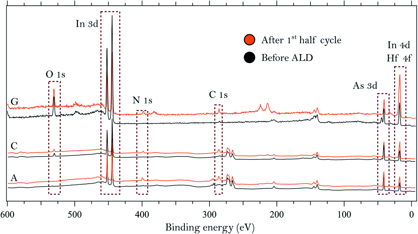 | ||
| Fig. 1 Survey spectra collected on three of the InAs samples using photon energies of 675 eV (samples A and C) and 900 eV (sample G). | ||
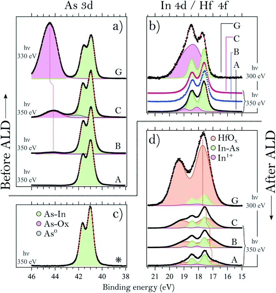 | ||
| Fig. 2 Core-level spectra before and after TDMAHf deposition. (a) As 3d spectra of samples A, B, C and G acquired before TDMAHf deposition. The green doublet is associated with As bonded to In, while the broad purple doublet is associated with As bonded to O. (b) In 4d spectra of samples A, B, C and G before TDMAHf deposition. The green doublet is associated with In bonded to As, while the broad purple doublet is associated with In bonded to O. For samples B and C, the fit is not shown since the line shape is identical to that of sample A. (c) As 3d spectrum of sample C after the first ALD half-cycle. Since the spectra of all other samples look the same as that of sample C, only this particular spectrum is shown. (d) In 4d and Hf 4f spectra acquired after TDMAHf deposition. Green fits indicate the In 4d bulk component of InAs (In bonded to As), purple (small) its oxide, and orange (large) the HfOx component. The vertical dotted line highlights the binding energy shift of the Hf 4f core level. (a–d) The photon energy used for measuring the spectra on samples A, B and C was 350 eV, while 330 and 300 eV were used for sample G. The spectra of sample G-H were collected at MAX-lab with a lower energy resolution (0.50 eV) in comparison to the spectra of samples A, B, C and D acquired at the MAX IV Laboratory (0.35 eV). | ||
In contrast to sample A, sample B – an InAs surface that had been exposed to 0.05 L of oxygen gas – shows a small As oxide component in the As 3d spectrum (cf.Fig. 2a). The component is located at 44.2 eV, i.e. at +3.2 eV higher binding energy than the InAs bulk component, in agreement with literature values.8,10,29,33–34 The lineshape of the In 4d line is identical to that of sample A (see Fig. 2b).
Sample C – an InAs surface exposed to 6 L O2 – differs from samples A and B, not only in terms of the expected more intense As oxide component due to the higher exposure to oxygen gas, but also by a small component at 42.0 eV, +1.0 eV above the bulk component (Fig. 2a). We assign this component to arsenic in the zero oxidation state, i.e. to As antisite defects or elemental As. This component is unexpected, since all samples were cut from the same InAs wafer, and sample C is the only one with an As0 component. Its contribution to the overall As intensity is less than 5%, and its origin is likely associated with a non-perfect homogeneity of the wafer. The line shape of the In 4d spectrum of sample C is identical to the one of sample A (cf.Fig. 2b).
Lastly, the As 3d and In 4d core levels of the sample exposed to 10 L of oxygen (sample D) exhibit the main As 3d component centred at 41.0 eV and its oxide at 44.0 eV, +3.0 eV above the bulk component. As for the other samples, the In 4d bulk component is found at 17.6 eV and its oxide at 18.1 eV, +0.5 eV from the bulk component; however, sample D is the only InAs sample with a thin layer of thermal oxide that shows slightly higher intensity (with respect to the bulk) of the In oxide.
From a comparison of all the examined thermal oxide samples, it is clear that the exposure time to O2 changes only the relative intensities of the As oxide and bulk components without changing the oxidation states of the surface. Indeed, we found that all As 3d oxide components are found at (+3.1 ± 0.1) eV from the InAs bulk component and the In 4d oxide ones at (+0.5 ± 0.1) eV above the bulk component. We also note that the relative binding energies of the oxide peak with respect to the bulk suggest that the As and In oxidation states are As3+ and In+, as in As2O3 and In2O. Interestingly, it appears as if exposure to O2 doses below 10 L mainly leads to oxidation of the As atoms, while the surface In atoms are left unchanged, including a bulk InAs component and a small amount of In oxide. Finally, the thickness of the thermal oxide layers can be evaluated from the intensity ratio between the oxide and bulk components.8 This is reported in Fig. 5 (first four points of the graph).
Turning to the samples with a thick, uniform native oxide layer, we find a common oxide stoichiometry for all of them; they only differ in the thickness of the oxide layer (see the Discussion section). The binding energies of the bulk and oxide components are found at values in excellent agreement with those found for samples A–D, except for the As 3d oxide. As is seen in Fig. 2a, the As oxide component of sample G is slightly shifted towards a higher binding energy with respect to the As oxide component of sample C. InAs oxides can contain As atoms in two different oxidation states, As3+ and As5+. The As 3d component of As5+ is found at a 1–2 eV higher binding energy12,33 than that of As3+. The shift of the As oxide peak of sample G towards a higher binding energy amounts to around +0.3 eV, and we attribute it to the presence of a small amount of As5+ suboxides, not observed for the other samples. For simplicity, we fitted the data with a single doublet only that includes the contribution of both the As3+ and As5+ oxidation states. The presence of an As5+ suboxide in the native oxide of sample G is not completely unexpected; we have observed it previously,21 and it is due to the lower homogeneity of the native oxide as compared to that of the thermal oxide layer.
To conclude this section, we find that the main difference between the analysed samples is the relative intensity of the oxide component with respect to the bulk peak, which has to be attributed to a different thickness of the oxide layer. Moreover, only the amount of As oxide differs for the samples with a thermal oxide.
Thermal and native oxides of InAs, during and after TDMAHf deposition
The core-level spectra collected after exposure of sample C to TDMAHf are shown in Fig. 2c and d. Additionally, in Fig. 4 we show the As 3d, In 4d and Hf 4f core level spectra acquired during the exposure, at a pressure of around 10−3 mbar. From Fig. 2C, it is seen that the As oxide of sample C gets fully removed by the interaction with TDMAHf. The observation is the same for all eight samples (not shown for the other seven samples), independent of the original quantity of the As oxide and its nature. The In 4d region (Fig. 2d) is more difficult to interpret. Here, a broad peak – the Hf 4f component – appears and overlaps with the In 4d peak. From a curve fit of this component we find the following Hf 4f binding energies: 17.1, 17.2, 17.4 and 17.5 eV for samples A, B, C and D, respectively, while it is 17.6 eV for all the other samples (E, F, G and H). Moreover, a small component of In oxide is visible in the In 4d/Hf 4f region for all examined samples. This is associated with an interface oxide, with the In oxide acting as As–In–O–Hf bridging bonds between bulk InAs and the HfOx8. It is important to highlight that all remaining In oxides get fully removed during the first TDMAHf deposition, independent of the original amount, similar to the behaviour of the As oxide. Thus, we can confirm here a perfect self-cleaning of all investigated samples already during the first ALD half-cycle, since the only remaining O atoms found afterwards are those needed to form the InAs–HfO2 interface.The time evolution of the exposure can be evaluated from time-resolved As 3d, In 4d, and Hf 4f ambient pressure XP spectra taken during TDMAHf exposure. They are shown for sample C in Fig. 4. Here, the origin of the timescale (0 min) is defined as the beginning of the data acquisition; the green dotted line, around 3 minutes, defines the moment when the TDMAHf exposure starts. The higher photon energy of 675 eV used in the acquisition of the time-resolved spectra, as compared to the As 3d and In 4d/Hf 4f spectra shown in Fig. 2, makes the measurements somewhat more bulk-sensitive and therefore less sensitive to the As oxide signal. The time-resolved data show clearly that the removal of the As oxide is rapid and that it coincides with the growth of HfOx in the Hf 4f signal. Hence, the spectra serve as a confirmation for the incorporation of the oxygen from the oxide of the InAs surface in the HfO2 layer.
Turning back to Fig. 2, we note that the H4 4f binding energies vary between the samples. The variation can be understood from the dependency of the binding energy on the chemical environment of the Hf ions. Recently, we found that the first reaction step during the early stage of HfO2 ALD by TDMAHf is a physisorption event, after which the Hf ion is still bound to all four ligands,8,35 indicated by a lower binding energy. The interaction with the surface is mediated by a lone pair of the nitrogen atoms. Later in the deposition, the Hf ion is partially bound to oxygen atoms (from the surface) and to some of its DMA− ligands, coming along with a shift to a higher binding energy. However, the binding energy of the Hf 4f line in stoichiometric HfO2 is found to be even higher.36–38 Therefore, we suppose that the Hf 4f binding energy observed here is a function of the average number of retained ligands: the larger the number of ligands, the lower the Hf 4f binding energy. This implies that with the increasing thickness of the original thermal oxide (samples A to D), a decreasing average number of ligands of the Hf precursor molecule is still retained after the first deposition.
It is also of interest to consider the molecular adsorbate species that appear on the surface upon interaction with TDMAHf. These species are easily identified from the N 1s core level spectra, shown for sample B in Fig. 3b. The spectrum shows a broad peak with two shoulders, one towards high and the other towards low binding energies. It is therefore deconvoluted with three identical Voigt profiles. For all samples, we find the main component at (399.0 ± 0.1) eV. This is due to photoemission from DMA− ligands. The shoulders at 400.8 eV (+1.8 eV from the main peak) and 397.3 eV (−1.7 eV) are assigned to dimethylamine (DMA) and methyl methylene imine (MMI).35,39,40 The relative intensities of the DMA−, DMA and MMI components vary somewhat between the samples, but in all cases the DMA− component is dominant with around 70% of the overall intensity, while the MMI and DMA peaks account for approximately 25% and 5% of the total N 1s intensity, respectively.
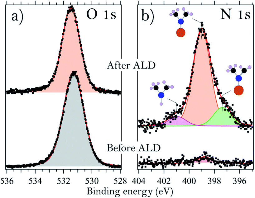 | ||
| Fig. 3 (a) O 1s core level spectra of sample G acquired at 660 eV photon energy before (bottom) and after (top) the first half ALD half cycle. (b) N 1s spectrum acquired before (bottom) and after (top) the first ALD half-cycle on sample B. The photon energy was 675 eV. The three fitted components are assigned to different ligands, as indicated by their sketched structures, where blue (black, grey, orange) circles correspond to N (C, H, Hf) atoms, respectively. | ||
 | ||
| Fig. 4 Series of (a) As 3d and (b) In 4d/Hf 4f ambient pressure XP spectra measured during the first half-cycle of ALD using a photon energy of 675 eV. The x axes represent the binding energy scale and the y axes show the acquisition time. The green dotted line indicates when the valve to the TDMAHf precursor was opened. The pressure after exposure start was approximately 10−3 mbar. The intensity is represented by a colour gradient from white (minimum) to blue (maximum). The colour scale is logarithmic in (a) so that the less intense As 3d oxide peak at around 44 eV binding energy is enhanced. It is linear in (b). | ||
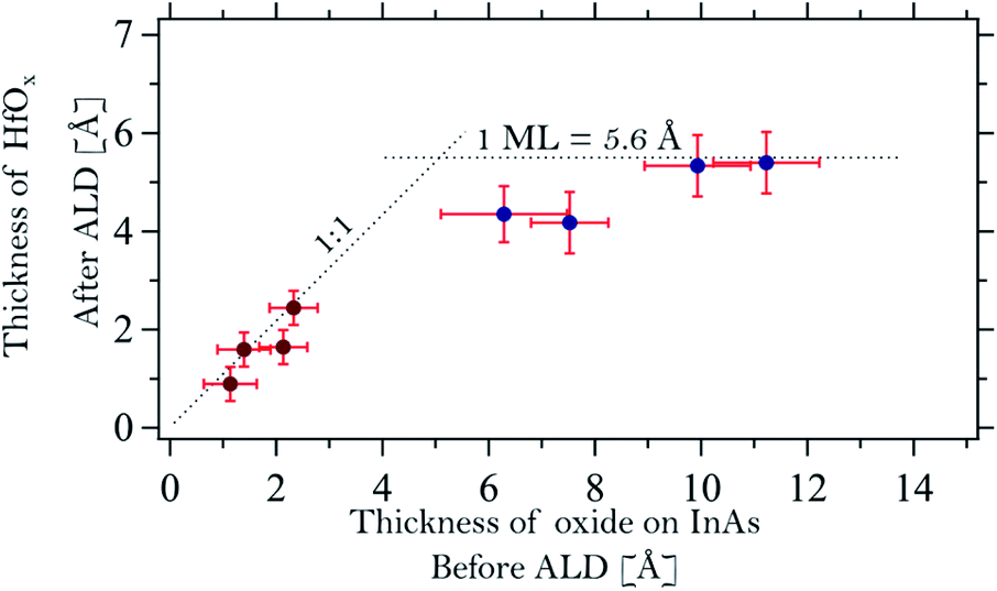 | ||
| Fig. 5 Correlation graph between the oxide thickness of InAs prior to the deposition and the thickness of the HfOx layer after the first half cycle. The samples are named alphabetically following their oxide thickness starting from the left (sample A). | ||
From a consideration of the In and As core levels, we find that the surface-adsorbed DMA− is most likely bound to Hf: no shift or extra components are visible in these core levels. MMI, together with an equal amount of DMA, is formed in elimination reactions of DMA− β-hydrides.39,41 However, the areas subtended by the peaks of MMI and DMA are dissimilar, and this suggests a partial desorption of DMA, justified by the high temperature used during deposition. Alternatively, DMA could, in principle, also be formed in a ligand exchange reaction. This latter reaction would, however, require the presence of surface hydroxyls.35,39
A careful analysis of the O 1s core level before and after the deposition of TDMAHf, as shown for sample G in Fig. 3a, results in one symmetric peak. Oxygen bonded to As, In, or Hf (in HfO2) cannot be distinguished since it results in the same binding energy. However, we can exclude the presence of any relevant amount of –OH groups, which would be visible as a separate O 1s component at a higher binding energy.10
Discussion
The functioning of ALD is based on the self-limiting interaction of gas-phase precursors with the surface onto which a thin layer of material should be deposited. Typically, the ALD of transition metal oxides is explained by invoking a ligand exchange reaction between the surface and the precursor molecules. The surface provides the active sites for this reaction in the form of surface hydroxyl groups, while the InAs substrate itself does not get involved. However, none of the examined InAs samples accommodate any hydroxyls. This is exemplified in Fig. 2a, which shows the O 1s core level spectrum of sample G. Clearly, the symmetric peak of O 1s does not exhibit any presence of –OH groups, which would lead to the appearance of a high-binding energy feature. Hence, we find that the standard ligand exchange reaction mechanism is not applicable to the initial ALD on the oxides of InAs.Instead, the role of the surface oxide needs to be taken into account. It is seen in Fig. 1 and 2c, d that the surface oxide has almost completely vanished after the deposition of TDMAHf; actually, from the time-resolved data in Fig. 4 it is apparent that the removal took place during the first few moments of TDMAHf exposure. At the same time, the O 1s peak does not change drastically in intensity: for example, the O 1s line of sample G, displayed in Fig. 3a, loses only around (18 ± 5)% of its intensity. The trend is the same for all investigated samples with a native oxide layer. This evidence suggests strongly that the oxygen atoms are transferred from the InAs oxide to the chemisorption layer: HfO2 is formed already in the first half-cycle of ALD.
As shown in Fig. 4, it is clearly possible to see how the component associated with arsenic oxide decreases after about 10 minutes from the exposure of the surface to the molecules and, with a slightly lower rate, the component associated with Hf 4f increases. The same behaviour is also observed for the time evolution APXPS measurement on sample D35 (not shown here), moreover, for that sample we observe a rate of reduction for the In 4d oxide peak similar to the one of the Hf 4f.
The phenomenon of oxygen transport and oxide formation without an external source is not included in any of the standard ALD models; instead, these models assume a static surface with O (or rather hydroxyl) sites to which the TDMAHf precursor binds after splitting off a ligand. Only the subsequent water deposition half-cycle provides additional O sites in the shape of hydroxyl groups, according to the models. Since the oxide thicknesses in our study vary strongly between the thermal and native oxide samples, we now consider the details of the oxygen transfer separately for the two types of oxides.
InAs with a thermal oxide: samples A, B, C and D
A model structure containing two different overlayers was used to estimate the thickness of the interface and HfOx layers on the InAs samples after TDMAHf deposition: the bulk InAs sample was assumed to be covered by an In2O interface layer, which in turn is capped by the HfOx layer. This model neglects the presence of molecular nitrogen and carbon materials on top of the surface. However, we consider that the DMA, DMA−, and MMI surface species containing N and C are always located at the outermost surface. Their influence on the attenuation of the Hf 4f, As 3d, and In 4d signals from different layers underneath is then identical, and can, therefore, be ignored in the layer thickness calculation. In the same way, the thickness of the thermal oxide layer on the InAs substrates prior to TDMAHf deposition was calculated. The calculations deliver an average thickness of 1.1, 1.4, 2.1 and 2.3 Å for samples A, B, C and D, respectively. Hence, the thermal oxide does not continuously cover the entire InAs surface, but rather consists of islands. Assuming that a monolayer of the oxide has a thickness of around 5 Å, estimated by an average of In2O and As3O5 oxides,42,43 this translates into surface coverages of 22%, 28%, 42% and 46%, respectively. Since the XP spectra were collected in several spots of the sample and no differences between the different spots were detected, we conclude that the oxide islands are significantly smaller than the size of the beam spot on the sample (100 × 100 μm2) and that they are distributed homogeneously on the sample surface.As is shown in Fig. 5 (dark red points at low oxide thickness) we find an excellent one-to-one correlation between the thickness of the final HfOx layer and that of the initial thermal oxide layer. A linear fit of the form THfOx = αTInAsOx was performed and a coefficient α = 0.95 ± 0.10 is found. In the formula, T is the thickness of the HfOx and the one of the oxide layer on InAs. Clearly, the amount of TDMAHf precursor material that interacts with the surface depends strictly on the quantity of thermal oxide prior to the deposition. The figure also shows that TDMAHf will interact only with the thermal oxide, but not with the clean InAs – otherwise, no correlation should be visible between the thickness of the initial InAs oxide layer and that of the final HfO2 layer, and we would expect to see thicker HfO2 layers also for samples with very thin thermal oxide layers.
The indium oxide component and the In 4d line shape, as shown in Fig. 2b, turn out to be the same prior to ALD for samples A, B and C. The main difference between them is the As oxide content. Interestingly, the amount of InOx is reduced upon TDMAHf deposition by only 35% (from 12% to 8% of the overall In 4d signal), which shows that almost the entire indium oxide present before deposition was needed to form the interface between the InAs and the HfOx. The As oxide, on the other hand, gets removed by 100% upon the initial ALD half-cycle.
For sample D, we also performed another half-cycle, executed with water vapour at 10−1 mbar. Interestingly, the InAs bulk component does not get re-oxidized during water deposition.35 This suggests that an initial Hf oxide coverage of around 50% is enough to produce a clean and sharp interface between HfO2 and InAs, which is uniform all along the surface and protected from re-oxidation during the water half-cycle.
Furthermore, after water deposition, a distinct hydroxyl peak was found in the O 1s spectra of sample D.35 This is another strong indication for the validity of the ligand exchange model after the first ALD cycle, even though we demonstrate here the limitation of the model during the initial ALD cycle.
InAs with a native oxide: samples E, F, G and H
The thickness of the initial native oxide layer on samples E, F, G, and H is estimated to be 6.3, 7.5, 9.9, and 11.2 Å, respectively. The thickness of the HfO2 layer after interaction with TDMAHf is also shown in Fig. 5 (blue data points). For these samples, the initial oxide thickness amounts to more than a monolayer. In contrast, the final HfO2 thickness appears to be limited to one monolayer. This behaviour contrasts with that of samples A to D. The fact that no As oxide is left after TDMAHf deposition requires that part of the oxygen atoms leave the surface in a parallel reaction. However, the exact mechanism involved is not clear, since our time-resolved in situ studies show that the rate of formation of HfOx and those of removal of the arsenic and indium oxide species are the same,8 independently on the thickness of the oxide layer on InAs. Further studies on the nature of the oxide layer and the formed interface, as well as the exact mechanism of the oxygen relocation, via structural characterization based e.g. on surface diffraction and theoretical models, are needed here. Nevertheless, the experimental observation that the thickness of the HfO2 layer after TDMAHf deposition is limited to one monolayer is important, as it confirms the self-limitation of ALD reactions, one of the basic ALD principles, even for the initial half-cycle.Conclusions
In conclusion, we report an oxygen transition from the oxide of InAs to the HfOx deposited by ALD using TDMAHf. Eight InAs samples, prepared with different oxide thicknesses, are analysed with in situ XPS. We find a linear correlation between the thickness of InAs oxide before deposition and the thickness of HfOx at the end of the first half cycle of ALD, self-limited though to a maximum of one monolayer of HfOx. Moreover, we observe that a 50% surface coverage of HfOx after the first half-cycle is enough to form a uniform interface which will, after further ALD cycles, result in a sharp and native oxide-free interface between the InAs substrate and the HfO2 layer.In contrast to the widely accepted ligand exchange model, we reveal that no surface hydroxyl groups are needed to initiate the ALD reaction of HfO2 formation on InAs.39 Instead, InAs oxide reacts readily with TDMAHf in the first half-cycle, irrespective of whether the oxide is native or thermal in nature, while pure InAs is inert with respect to an interaction with the TDMAHf ALD precursor.
Even though the surface structure of the InAs substrate prior to ALD and possible pre-treatments does influence the thickness of the HfOx layer after the first ALD half-cycle, which is not included in the ideal ALD models, we want to highlight that we observe an apparently perfect self-cleaning upon the first half-cycle over a broad range of initial InAs substrate configurations, if the initial deposition process is given sufficient time. This result is highly promising for the further development of high-speed, InAs-based MOSFET devices with improved III–V/high-κ interface quality.
Author contributions
G. D’A.: conceptualization, methodology, software, validation, formal analysis, investigation, writing – original draft, writing – review & editing, visualization. P. S., E. K., V. B., F. R. and N. M.: investigation, writing – review & editing. E. L., J. S., and R. T.: conceptualization, methodology, validation, formal analysis, investigation, writing – original draft, writing – review & editing, visualization.Conflicts of interest
There are no conflicts to declare.Acknowledgements
We acknowledge the MAX IV Laboratory for time on beamline SPECIES under Proposal 20200396. Research conducted at the MAX IV Laboratory, a Swedish national user facility, is supported by Vetenskapsrådet (Swedish Research Council) under contract 2018-07152, Vinnova (Swedish Governmental Agency for Innovation Systems) under contract 2018-04969 and Formas under contract 2019-02496. The staff at MAX IV are gratefully acknowledged for assistance in the beamtimes. We acknowledge project funding from Vetenskapsrådet, grant no. 2016-6186, 2017-03871 and 2017-4108. This work was further supported by the NanoLund Center for Nanoscience at Lund University.References
- M. Graef, International Roadmap for Devices and Systems - More than Moore - IRDS, https://irds.ieee.org/editions/2020 Search PubMed.
- P. D. Ye, G. D. Wilk, J. Kwo, B. Yang, H. J. L. Gossmann, M. Frei, S. N. G. Chu, J. P. Mannaerts, M. Sergent, M. Hong, K. K. Ng and J. Bude, IEEE Electron Device Lett., 2003, 24, 209–211 CAS.
- J. A. Del Alamo, Nature, 2011, 479, 317–323 CrossRef CAS PubMed.
- H. Ko, K. Takei, R. Kapadia, S. Chuang, H. Fang, P. W. Leu, K. Ganapathi, E. Plis, H. S. Kim, S. Y. Chen, M. Madsen, A. C. Ford, Y. L. Chueh, S. Krishna, S. Salahuddin and A. Javey, Nature, 2010, 468, 286–289 CrossRef CAS PubMed.
- J. Wu, A. S. Babadi, D. Jacobsson, J. Colvin, S. Yngman, R. Timm, E. Lind and L. E. Wernersson, Nano Lett., 2016, 16, 2418–2425 CrossRef CAS PubMed.
- S. M. Sze and K. K. Ng, in Physics of Semiconductor Devices, John Wiley & Sons, Inc., 2006, pp. 789–789 Search PubMed.
- K. Zhang, G. R. Zhu, Y. C. Kong, and T. S. Chen, 2018 Int. Conf. Microw. Millim. Wave Technol. ICMMT 2018 - Proc., 2018, vol. 39, pp. 179–180 Search PubMed.
- G. D’Acunto, A. Troian, E. Kokkonen, F. Rehman, Y. P. Liu, S. Yngman, Z. Yong, S. R. McKibbin, T. Gallo, E. Lind, J. Schnadt and R. Timm, ACS Appl. Electron. Mater., 2020, 2, 3915–3922 CrossRef.
- R. Timm, A. Fian, M. Hjort, C. Thelander, E. Lind, J. N. Andersen, L. E. Wernersson and A. Mikkelsen, Appl. Phys. Lett., 2010, 97, 132904 CrossRef.
- R. Timm, A. R. Head, S. Yngman, J. V. Knutsson, M. Hjort, S. R. McKibbin, A. Troian, O. Persson, S. Urpelainen, J. Knudsen, J. Schnadt and A. Mikkelsen, Nat. Commun., 2018, 9, 1412 CrossRef PubMed.
- L. Ye and T. Gougousi, Appl. Phys. Lett., 2014, 105, 121604 CrossRef.
- A. P. Kirk, M. Milojevic, J. Kim and R. M. Wallace, Appl. Phys. Lett., 2010, 96, 202905 CrossRef.
- C. L. Hinkle, A. M. Sonnet, E. M. Vogel, S. McDonnell, G. J. Hughes, M. Milojevic, B. Lee, F. S. Aguirre-Tostado, K. J. Choi, H. C. Kim, J. Kim and R. M. Wallace, Appl. Phys. Lett., 2008, 92, 071901 CrossRef.
- S. M. George, Chem. Rev., 2010, 110, 111–131 CrossRef CAS PubMed.
- J. A. Raiford, S. T. Oyakhire and S. F. Bent, Energy Environ. Sci., 2020, 13, 1997–2023 RSC.
- A. S. Asundi, J. A. Raiford and S. F. Bent, ACS Energy Lett., 2019, 4, 908–925 CrossRef CAS.
- J. Plutnar and M. Pumera, Small, 2021, 17, 2102088 CrossRef CAS PubMed.
- F. Zaera, Coord. Chem. Rev., 2013, 257, 3177–3191 CrossRef CAS.
- N. E. Richey, C. De Paula and S. F. Bent, J. Chem. Phys., 2020, 152, 040902 CrossRef CAS PubMed.
- H. H. Sønsteby, A. Yanguas-Gil and J. W. Elam, J. Vac. Sci. Technol., A, 2020, 38, 020804 CrossRef.
- A. Troian, J. V. Knutsson, S. R. McKibbin, S. Yngman, A. S. Babadi, L. E. Wernersson, A. Mikkelsen and R. Timm, AIP Adv., 2018, 8, 125227 CrossRef.
- J. Schnadt, J. Knudsen and N. Johansson, J. Phys.: Condens. Matter, 2020, 32, 413003 CrossRef CAS PubMed.
- E. Kokkonen, F. L. Da Silva, M. H. Mikkela, N. Johansson, S. W. Huang, J. M. Lee, M. Andersson, A. Bartalesi, B. N. Reinecke, K. Handrup, H. Tarawneh, R. Sankari, J. Knudsen, J. Schnadt, C. Sathe and S. Urpelainen, J. Synchrotron Radiat., 2021, 28, 588–601 CrossRef CAS PubMed.
- S. Urpelainen, C. Säthe, W. Grizolli, M. Agäker, A. R. Head, M. Andersson, S. W. Huang, B. N. Jensen, E. Wallén, H. Tarawneh, R. Sankari, R. Nyholm, M. Lindberg, P. Sjöblom, N. Johansson, B. N. Reinecke, M. A. Arman, L. R. Merte, J. Knudsen, J. Schnadt, J. N. Andersen and F. Hennies, J. Synchrotron Radiat., 2017, 24, 344–353 CrossRef CAS PubMed.
- J. Schnadt, J. Knudsen, J. N. Andersen, H. Siegbahn, A. Pietzsch, F. Hennies, N. Johansson, N. Mårtensson, G. Öhrwall, S. Bahr, S. Mähl and O. Schaff, J. Synchrotron Radiat., 2012, 19, 701–704 CrossRef CAS PubMed.
- R. Denecke, P. Väterlein, M. Bässler, N. Wassdahl, S. Butorin, A. Nilsson, J. E. Rubensson, J. Nordgren, N. Mårtensson and R. Nyholm, J. Electron Spectrosc. Relat. Phenom., 1999, 101–103, 971–977 CrossRef CAS.
- M. Hjort, J. V. Knutsson, B. Mandl, K. Deppert, E. Lundgren, R. Timm and A. Mikkelsen, Nanoscale, 2015, 7, 9998–10004 RSC.
- G. Hollinger, R. Skheyta-Kabbani and M. Gendry, Phys. Rev. B, 1994, 49, 11159–11167 CrossRef CAS PubMed.
- D. M. Poirier and J. H. Weaver, Surf. Sci. Spectra, 1993, 2, 224–231 CrossRef CAS.
- D. Y. Petrovykh, M. J. Yang and L. J. Whitman, Surf. Sci., 2003, 523, 231–240 CrossRef CAS.
- L. Olsson, L. Ilver, J. Kanski, P. Nilsson, C. Andersson and U. Karlsson, Phys. Rev. B: Condens. Matter Mater. Phys., 1996, 53, 4734–4740 CrossRef CAS PubMed.
- B. Brennan and G. Hughes, J. Appl. Phys., 2010, 108, 053516 CrossRef.
- R. Timm, M. Hjort, A. Fian, C. Thelander, E. Lind, J. N. Andersen, L. E. Wernersson and A. Mikkelsen, Microelectron. Eng., 2011, 88, 1091–1094 CrossRef CAS.
- L. Ley, R. A. Pollak, F. R. McFeely, S. P. Kowalczyk and D. A. Shirley, Phys. Rev. B, 1974, 9, 600–621 CrossRef CAS.
- G. D’Acunto, P. Shayesteh, E. Kokkonen, V. Boix, F. Rehman, N. Mosahebfard, E. Lind, J. Schnadt and R. Timm, in Manuscr, 2022 Search PubMed.
- O. Renault, D. Samour, J. F. Damlencourt, D. Blin, F. Martin, S. Marthon, N. T. Barrett and P. Besson, Appl. Phys. Lett., 2002, 81, 3627–3629 CrossRef CAS.
- J. C. Lee, S. J. Oh, M. Cho, C. S. Hwang and R. Jung, Appl. Phys. Lett., 2004, 84, 1305–1307 CrossRef CAS.
- G. Aygun and I. Yildiz, J. Appl. Phys., 2009, 106, 014312 CrossRef.
- G. D’Acunto, R. Tsyshevsky, P. Shayesteh, J.-J. Gallet, F. Bournel, F. Rochet, I. Pinsard, R. Timm, A. R. Head, M. Kukla and J. Schnadt, In Manuscr, 2022 Search PubMed.
- A. R. Head, S. Chaudhary, G. Olivieri, F. Bournel, J. N. Andersen, F. Rochet, J. J. Gallet and J. Schnadt, J. Phys. Chem. C, 2016, 120, 243–251 CrossRef CAS.
- A. R. Head, S. Chaudhary, G. Olivieri, F. Bournel, J. N. Andersen, F. Rochet, J. J. Gallet and J. Schnadt, J. Phys. Chem. C, 2016, 120, 243–251 CrossRef CAS.
- P. Villars, Inorganic Solid Phases, SpringerMaterials (online database), https://materials.springer.com/isp/crystallographic/docs/sd_1714120 Search PubMed.
- L. Liu, C. C. He, J. Zeng, Y. H. Peng, W. Y. Chen, Y. J. Zhao and X. B. Yang, J. Phys. Chem. C, 2021, 125, 7077–7085 CrossRef CAS.
| This journal is © The Royal Society of Chemistry 2022 |