
 Open Access Article
 This Open Access Article is licensed under a Creative Commons Attribution-Non Commercial 3.0 Unported Licence
Design of semitransparent tantalum nitride photoanode for efficient and durable solar water splitting†
Tomohiro
Higashi
 *a,
Hiroshi
Nishiyama
b,
Vikas
Nandal
*c,
Yuriy
Pihosh
b,
Yudai
Kawase
d,
Ryota
Shoji
e,
Mamiko
Nakabayashi
f,
Yutaka
Sasaki
b,
Naoya
Shibata
f,
Hiroyuki
Matsuzaki
e,
Kazuhiko
Seki
c,
Kazuhiro
Takanabe
d and
Kazunari
Domen
*bg
*a,
Hiroshi
Nishiyama
b,
Vikas
Nandal
*c,
Yuriy
Pihosh
b,
Yudai
Kawase
d,
Ryota
Shoji
e,
Mamiko
Nakabayashi
f,
Yutaka
Sasaki
b,
Naoya
Shibata
f,
Hiroyuki
Matsuzaki
e,
Kazuhiko
Seki
c,
Kazuhiro
Takanabe
d and
Kazunari
Domen
*bg
aInstitute for Tenure Track Promotion, University of Miyazaki, Nishi 1-1 Gakuen-Kibanadai, Miyazaki, 889-2192, Japan. E-mail: t_higashi@cc.miyazaki-u.ac.jp
bOffice of University Professors, The University of Tokyo, 2-11-16 Yayoi, Bunkyo-ku, Tokyo 113-8656, Japan. E-mail: domen@chemsys.t.u-tokyo.ac.jp
cGlobal Zero Emission Research Center, National Institute of Advanced Industrial Science and Technology, Tsukuba 16-1 Onogawa, Ibaraki 305-8569, Japan. E-mail: nk.nandal@aist.go.jp
dDepartment of Chemical System Engineering, School of Engineering, The University of Tokyo, 7-3-1 Hongo, Bunkyo-ku, Tokyo 113-8656, Japan
eResearch Institute for Material and Chemical Measurement, National Metrology Institute of Japan (NMIJ), National Institute of Advanced Industrial Science and Technology, Tsukuba, 1-1-1 Higashi, Tsukuba, Ibaraki 305-8565, Japan
fInstitute of Engineering Innovation, The University of Tokyo, 2-11-16 Yayoi, Bunkyo-ku, Tokyo 113-8656, Japan
gResearch Initiative for Supra-Materials (RISM), Shinshu University, 4-17-1 Wakasato, Nagano 380-8533, Japan
First published on 7th October 2022
Abstract
Unbiased solar water splitting via a photoelectrochemical–photovoltaic (PEC–PV) tandem device is a promising strategy for efficient, low-cost, and sustainable hydrogen production to address growing energy demands. The bandgap of Ta3N5 is 2.1 eV for a theoretical limit of solar-to-hydrogen (STH) energy conversion efficiency of 15.3%, but the inefficient utilization of photogenerated holes limits the STH efficiency to 7% when Ta3N5 is used as a single photoanode. In addition, the formation of a TaOx insulating layer on the bare Ta3N5 surface caused by the self-photooxidation of the Ta3N5 surfaces leads to the poor stability of the water oxidation reaction. In this study, we fabricated a void-free Ta3N5 planar thin film, originating from metallic Ta deposition by high-power sputtering followed by nitridation in ammonia treatment at high temperature, grown on a transparent GaN/Al2O3 substrate. With the uniform decoration of the Ta3N5 surface with an ultrathin NiFeOx electrocatalyst layer, the semitransparent Ta3N5 photoanode drastically improved the stability and generated a photocurrent of 7.4 mA cm−2 at 1.23 V vs. a reversible hydrogen electrode under simulated AM1.5G solar illumination. Unassisted water splitting by a transparent Ta3N5 photoanode coupled with CuInSe2 PV was demonstrated with an initial STH efficiency of 9%, which is the highest efficiency ever reported among metal oxide/nitride-based PEC–PV tandem cells. With the homogeneous electrocatalyst, the tandem cell achieved the stabilized STH efficiency of 4% up to 2 h of device operation. Using measurements and theoretical modeling, the charge carrier kinetics and transport were determined to identify the most crucial Ta3N5-thin-film parameters for further performance enhancement.
Broader contextHarvesting solar energy via photocatalytic and photoelectrochemical (PEC) water-splitting technology is an emerging solution to produce cost-effective and carbon-free hydrogen and oxygen fuels for sustainable global development. Photovoltaic (PV)-biased PEC water splitting is an effective strategy for achieving a solar-to-hydrogen (STH) energy conversion efficiency of more than 10%, which is essential for commercial solar hydrogen production. To date, the reported STH energy conversion efficiency of well-recognized metal oxides or nitride photoelectrode-based PEC–PV tandem water splitting systems (lead-free and single semiconductor-electrolyte junction) is less than 7%. Considering the advancements in PV technologies, the STH energy conversion efficiency of tandem devices remains challenging owing to limited visible light absorption and inefficient utilization of photogenerated holes inside photoelectrode materials for water oxidation. Herein, we demonstrate that a polycrystalline void-free Ta3N5 thin-film (covered with a homogenous NiFeOx electrocatalyst) semitransparent photoelectrode eliminates the abovementioned challenges and realizes a photocurrent of 7.4 mA cm−2 at 1.23 V vs. a reversible hydrogen electrode under simulated AM1.5G solar illumination. The visible-light-absorbing NiFeOx/Ta3N5 semitransparent photoelectrode and two-series-connected CuInSe2 solar cells drove unbiased overall water splitting with an initial STH energy conversion efficiency of 9%. Our work represents a significant advancement in maximizing the potential of visible-light photoabsorbers and approaching the efficiency targets for practical solar hydrogen production. |
1. Introduction
The photoelectrochemical (PEC) water splitting reaction is widely recognized as one of the most promising methods for the sustainable generation of hydrogen and oxygen gases (suitable for storage and transportation) from solar energy and water.1–5 Typically, the PEC system is comprised of a light-absorbing photoelectrode (defined as the working electrode (WE)), which is serially connected via electrical bias with the counter electrode (CE). The operation of a PEC system requires solar and electrical energy to maximize the solar-to-hydrogen (STH) energy conversion efficiency from overall water splitting (OWS). Despite visible-light photon absorption, the applied-bias photon-to-current efficiency (ABPE) for the oxygen evolution reaction (OER) has been restricted to 3.25% among metal oxide/nitride-based photoanodes.6,7 Between WE and CE, the Photovoltaic (PV) cells are an attractive strategy for converting sunlight to the required electrical bias for OWS. Such a PEC–PV tandem device comprises series-connected wide-bandgap and narrow-bandgap semiconducting materials at the top and bottom, respectively. During device operation, the incident AM1.5G solar spectrum is harvested up to the bandgap energy of the top semiconductor, and the rest of the transmitted spectrum is absorbed by the bottom semiconductor to generate a matched OWS current density. Consequently, the STH energy conversion efficiency of a tandem device is governed by a wide-bandgap semiconductor (top), which has relatively less light absorption than a narrow-bandgap semiconductor (bottom).8,9 The PEC–PV tandem configuration facilitates solar water splitting without any external electrical bias and is therefore considered as a promising candidate for realizing high STH energy conversion efficiency up to theoretical limits of ∼40%10–12 and 26% (see Fig. S1, ESI†) at fixed bottom narrow-bandgap semiconductor of 0.4 eV and 1.12 eV, respectively. The development of narrow-bandgap photoelectrodes for visible-light absorption and efficient charge utilization is crucial and achieving a high STH energy conversion efficiency of more than 10% for commercial STH production is challenging.Various materials have been designed for the cost-effective development of tandem devices to realize unassisted OWS. For instance, wide-bandgap metal oxides/nitrides such as WO3,13–15 BiVO4,15–20 Fe2O3,21–23 and Ta3N57,24–26 based photoanodes have been extensively examined for the OER. In addition, perovskite oxides (BaSnO3)27 and PV grade materials (like silicon) have been developed as photoanodes28–30 to generate the photocurrent density over 10 mA cm−2 at 1.23 V vs. a reversible hydrogen electrode (VRHE) under AM1.5G solar illumination. The Si-based photoanode exhibited a stabilized photocurrent density of 20 mA cm−2 for 100 h of continuous operation.28–30 However, these photoanodes based on PV grade materials have a non-transparent structure, and therefore, not suitable for tandem-type unassisted OWS. Thus, the development of the visible-light-absorbing semitransparent photoanode is a prerequisite for the application of the tandem-type OWS cell. A lot of studies have attempted to develop visible-light-absorbing semitransparent photoanodes based on Fe2O3, BiVO4, metal ferrite, and Ta3N5 that can be applicable for the tandem-type PEC–PV cells.8,31 Moreover, narrow-bandgap semiconductors such as chalcogenides,32–34 silicon,35,36 dye-sensitized solar cells (DSCs),13,14 and perovskite solar cells (PSCs)37–39 were employed either as photocathodes or photovoltaic cells in tandem devices for the hydrogen evolution reaction (HER). Recently, Park et al. achieved the highest reported STH of 4.49% in Ti- and Si-codoped Fe2O3 semitransparent photoanode coupled with PSC.40 Wang et al. showed an impressive STH energy conversion efficiency of 6.5% from dual-BiVO4 photoanodes and PSCs-based tandem device.37 Besides, Table S1 (ESI†) presents the summary on the recent developments of PEC–PV tandem device. To achieve an STH energy conversion efficiency of 10%, the light absorption edge of the front semitransparent photoanode should be in the wavelength range of 527 nm to 946 nm at an external quantum efficiency (EQE) of 100% and narrow-bandgap energy of 1.12 eV (see Fig. S1b, ESI†).
Tantalum nitride (Ta3N5) with a bandgap energy of 2.1 eV is a promising candidate for absorbing solar light up to a wavelength of 600 nm with a theoretical STH energy conversion efficiency limit of 15.26% at an EQE of 100%.25,41–43 These light absorption features and appropriate energy level alignment with the water redox potential have prompted significant research on different Ta3N5-based solar water splitting technologies such as photocatalyst sheets, Z-schemes, PEC cells, and tandem devices for water splitting activity. Wang et al. demonstrated OWS from the heterojunction of single crystalline Ta3N5 nanorods with KTaO3 particles.44 In a different study, Wang et al. displayed the potential of Ta3N5 (modified with Ir and CoOx electrocatalysts) for OER with its counterpart La and Rh co-doped SrTiO3 for HER in Z-scheme system.45 Moreover, our group showed that the OER activity of non-transparent Ta3N5 nanorods (Ta3N5-NRs), loaded with FeNiOx electrocatalyst, photoanode was significantly improved by suppressing fundamental loss mechanisms to realize half-cell STH (HC-STH) energy conversion efficiency of 2.7%.7 The onset potential of such efficient photoanode was ∼0.57 VRHE, which could be limited by the surface defect states of Ta3N5.7,46 The onset potential of non-doped Ta3N5-based photoanodes were typically reported in the range of ∼0.5–0.8 VRHE.8,24–26 The surface passivation (by TiO2 and GaN)47–49 and low-valence cation (such as Zr, Mg, Sc, Ba, and B)6,50–54 dopant engineering of Ta3N5 enabled the lowering of onset potential for OER activity. Besides this, the BaTaO2N/Ta3N5 heterostructure based photoanode could reduce the onset potential by selectively transferring the holes from Ta3N5 to electrolyte for OER activity.54
Ta3N5 material is generally processed by heating the precursor compounds (like Ta2O5, TaOδ, and Ta metal) in an ammonia (NH3) atmosphere at high temperature close to 1000 °C.7,26,47 Typically, such harsh high temperature processing deteriorated the commercially available visible-light-transparent conductive substrates such as indium tin oxide (ITO) and fluorine-doped tin oxide (FTO) and led to low conductivity and the transparency.55 To overcome this problem, Ta3N5 films were developed on the chemically durable transparent substrates such as Ta-doped TiO2,56 carbon nanotube film-coated quartz,52 GaN-coated sapphire,57 and synthetic quartz.26 In addition, the Ta3N5 film was prepared directly on FTO substrate by using an atomic layer deposition technique, however, the light absorption in long wavelength range was limited by film thickness.58 Recently, our group developed a Ta3N5 planar thin film (loaded with NiFeOx electrocatalyst) on transparent n-type GaN-coated sapphire (GaN/Al2O3) substrate for OER.57 The GaN/Al2O3 substrate displayed excellent electrical and optical properties after the deposition of Ta3N5 thin film under high temperature nitridation condition. Additionally, n-type GaN layer conjugated with Ta3N5 acts as a hole-blocking layer to suppress electron–hole recombination, resulting in enhanced photocurrent density for OER activity.57 The developed semitransparent Ta3N5/GaN/Al2O3 photoanode was wired with two series-connected (dual) CuInSe2 (CIS) photovoltaic cells (integrated with Pt/Ni electrocatalyst) for HER activity.57 This Ta3N5-CIS tandem cell initially provides a STH energy conversion efficiency of 7%, which reduces to 5.5% after 15 minutes of device operation.57 The decrease in STH energy conversion efficiency primarily originated from the performance degradation of the Ta3N5 photoanode. During device operation, the photogenerated holes were migrated to the Ta3N5/water interface and drove the oxidation to form the thin layer of TaOx at the interface.46,47,55,59 The insulating electrical properties of the TaOx layer suppressed the holes transport from Ta3N5 to water, and hence, degraded the efficiency of OER. Surface modification with an electrocatalyst layer or/and with a protection layer is an excellent strategy to reduce the photooxidation of Ta3N5.8 For instance, Kawase et al. improved the long-term durability (with current retention of 80% after 2 hours of continuous operation) of Ta3N5 photoanode by coating a NiFeOx electrocatalyst with high surface coverage.59 Although increased OER was detected with high surface coverage by NiFeOx (amount exceeding threshold of 0.1 μmol cm−2), the light transmission from a photoanode above 600 nm (light absorption edge) was significantly reduced to less than 40%,59 indicating that the simultaneous realization of good transparency/absorption and large surface coverage by electrocatalysts remains problematic for achieving high STH energy conversion efficiency and long-term durability from tandem devices for practical STH production.
In this study, we developed an efficient OWS and improved the durability of Ta3N5-based tandem cells. In particular, the STH energy conversion efficiency of tandem cells has increased with the development of high-quality void-free Ta3N5 photoactive thin film on transparent GaN/Al2O3 substrate. The n-type GaN layer functions as an electron collection layer as well as hole-blocking layer to suppress the electron–hole recombination at the interface of metal contact and GaN layer. The uniform loading of the NiFeOx electrocatalyst over the Ta3N5 surface stabilized the OER activity for a longer time by suppressing self-photooxidation during continuous device operation. With conventional low-input-power radio-frequency magnetron sputtering (RF-MS), the fabricated Ta3N5 thin film has a significant number of voids across the film thickness. These voids could act as recombination or trapping centers for photogenerated charge carriers and limit OER activity. The high kinetic energy of the incident target atoms is required to produce a highly dense film on the substrate.60,61 The kinetic energy of the deposited atoms can be controlled as a function of the level of input-power of RF-MS. High-quality (void-free) Ta3N5 thin film was obtained using an optimized high-input-power RF-MS technique. Moreover, the distribution of the NiFeOx electrocatalyst over the Ta3N5 surface was varied using drop-casting and spin-coating deposition methods.59 Uniform and non-uniform deposition of the electrocatalyst were achieved by spin-coating and drop-casting methods, respectively. The influence of the above Ta3N5 and electrocatalyst processing techniques on the material, PEC, and stability features was demonstrated.
The optimized NiFeOx/Ta3N5/GaN/Al2O3 photoanode prepared by high-input-power RF-MS and spin-coating processes generates photocurrent density of 7.4 mA cm−2 at 1.23 VRHE, under simulated AM1.5G solar illumination. A photocurrent gain of 1.1 mA cm−2 is realized by suppressing the void density inside the Ta3N5 thin film. With the drop-casting method, the photocurrent decayed rapidly to almost zero within 30 min, whereas an improved photocurrent retention of ∼4 mA cm−2 after 1.5 h was achieved using the spin-coating method. Furthermore, the tandem device was designed with an optimized Ta3N5-based photoanode and two series-connected CuInSe2 elements to display bias-free OWS. The developed Ta3N5-CuInSe2 tandem cell exhibited an initial STH energy conversion efficiency of 9.0%, which is higher than that of previously reported WO3-, Fe2O3-, BiVO4-, and Ta3N5-based tandem devices (Table S1 and Fig. S2, ESI†). Because the STH energy conversion efficiency of 4% up to 2 h is maintained, this work presents the critical role of homogeneous electrocatalyst coating for the enhanced durability of efficient tandem systems. Furthermore, transient absorption spectroscopy (TAS) measurements of the Ta3N5 thin film were performed to probe the decay kinetics of photogenerated charge carriers in the picosecond to microsecond time range. Various unreported material/device parameters and dominant loss mechanisms were determined by modelling the TAS and PEC characteristics. These Ta3N5 specifications are essential for developing design schemes for performance optimization and realizing STH energy conversion efficiencies beyond 10%.
2. Results and discussion
2.1. Material properties of Ta3N5 photoanode
The Ta3N5/GaN/Al2O3 thin-film samples fabricated using low- and high-input-power RF-MS were characterized by X-ray diffraction (XRD) and scanning transmission electron microscopy (STEM) analysis. Details of the fabrication processes and characterizations are included in the Materials and methods section of the ESI.†Fig. 1a displays the measured XRD patterns of the Ta3N5/GaN/Al2O3, GaN/Al2O3 substrate, and Ta3N5 powder reference (DB01-089-5200). The XRD patterns of the Ta3N5/GaN/Al2O3 samples were comprised of crystalline phases of Ta3N5 and GaN/Al2O3 substrates. The XRD peak at 24.2° was assigned to the main (110) crystal plane of Ta3N5. Subnitride impurities, such as TaN and Ta3N6 phases, were absent in the developed specimen. Crystalline Ta3N5 thin films were successfully prepared on a GaN/Al2O3 substrate regardless of the input RF power. The GaN/Al2O3 substrate shows a strong XRD peak at 34° from the (002) plane, indicating a single-crystalline GaN-epitaxial film on the Al2O3 layer. However, the peak intensity of the Ta3N5 thin film was weaker than that of the GaN/Al2O3 substrate. The XRD patterns derived from the Ta3N5 thin film are consistent with the Ta3N5 powder reference and reported literature.62 These results indicate that the low- and high-input-power RF-MS developed polycrystalline Ta3N5 films on the GaN/Al2O3 substrates.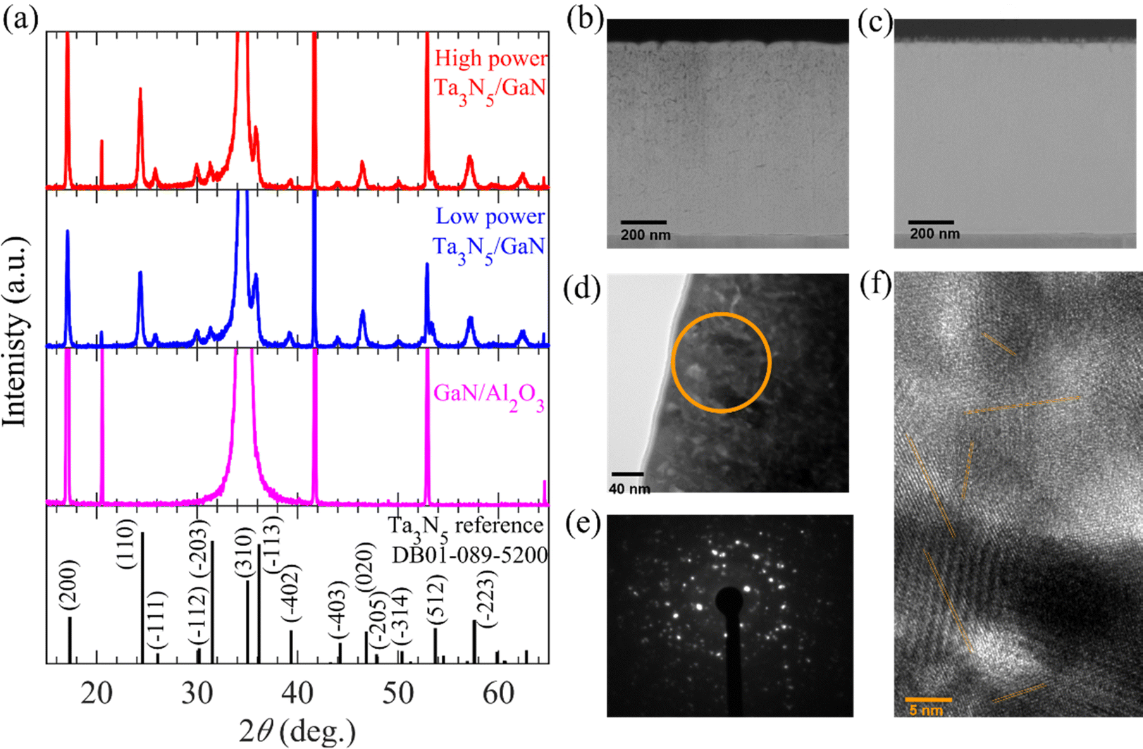 | ||
| Fig. 1 Crystalline and structural properties of Ta3N5/GaN/Al2O3 specimen. (a) XRD patterns of Ta3N5/GaN/Al2O3 (fabricated by high and low input RF power sputtering), GaN/Al2O3 substrate, and Ta3N5 reference (DB01-089-5200). Cross-sectional ADF-STEM images of Ta3N5 thin film (with thickness of ∼800 nm) developed using (b) low and (c) high-input-power RF-MS on GaN layer. (d) Cross-sectional TEM image of Ta3N5 prepared by high-input-power RF-MS. (e) SAED of the circle shown in the TEM image of panel (d). (f) HRTEM image of Ta3N5/GaN/Al2O3. Various parallel lines represent different crystal planes of Ta3N5. | ||
Fig. 1(b) and (c) show the cross-sectional annular dark field STEM (ADF-STEM) images of the Ta3N5/GaN/Al2O3 samples. With low- and high-input-power RF-MS, a similar Ta3N5 film thickness of 800 nm was developed on the GaN/Al2O3 substrate. This development indicates that the apparent deposition rate of the Ta precursor growth on the substrate from high-input-power RF-MS is comparable to that of low-input-power RF-MS. Fig. S3 in the ESI† illustrates the intermittent switching of high input RF power (from continuous sinusoidal wave to zero level) using a function-generating apparatus compared to the conventional low-input-power RF-MS. The deposition rate during high-input-power RF-MS was adjusted to make the average deposition rate over the intermittent switching comparable to that of the continuous low-input-power RF-MS, leading to a similar apparent deposition rate of the precursor, and hence, the Ta3N5 thickness. Moreover, the cross-sectional ADF-STEM images (in Fig. 1b) present significant voids or pinholes from the middle to the surface region of Ta3N5 for low-input-power RF-MS, whereas a high-quality Ta3N5 film without any pinholes is obtained by high-input-power RF-MS (Fig. 1c). From cross-sectional transmission electron microscopy (TEM; Fig. 1d), selected-area electron diffraction (SAED; Fig. 1e), and high-resolution TEM (HRTEM; Fig. 1f) analysis, the Ta3N5 film prepared from high-input-power RF-MS is polycrystalline and comprises clustered Ta3N5 domains with nanometer-sized crystalline grains oriented in multiple directions. As shown in Fig. S4 of the ESI,† the two-dimensional fast Fourier transforms (FFT) in several specified areas indicate that the small-sized single-crystalline Ta3N5 with several orientations was distributed over a wide area, which is evident from the bright spots (with varying intensities) originating from different crystalline planes (orientations) of Ta3N5 clusters. The single-crystal domains of Ta3N5 with different orientations were well separated. These results indicate that multiple crystal grains with different lattice orientations are assembled to form polycrystalline Ta3N5 thin films.
Using drop-casting and spin-coating methods (Fig. S5(b) and (c), ESI†), the NiFeOx electrocatalyst was loaded onto the surface of the Ta3N5/GaN/Al2O3 samples to promote the OER and the stability of the photoanode. Coverage of the Ta3N5 surface by the electrocatalyst could be a crucial factor in determining the durability of the OER. To demonstrate this hypothesis, the NiFeOx is deposited on the Ta3N5 surface by either of the above procedures, i.e., drop-casting or spin-coating. Fig. 2(a) and (b) show the top-view of SEM images of Ta3N5 thin films modified with NiFeOx through drop-casting and spin-coating, respectively. Using the drop-casting method, the SEM image of the NiFeOx/Ta3N5 specimen indicated separate dark and bright regions corresponding to NiFeOx deposits and bare Ta3N5, respectively. Such random deposition of NiFeOx species on the Ta3N5 surface and the emergence of bare Ta3N5 is attributed to the non-uniform nucleation-growth process during solvent evaporation. The direct contact of bare Ta3N5 surfaces with an aqueous electrolyte solution facilitates the photooxidation process upon solar illumination, which leads to insulating TaOx formation and consequently reduces the OER activity.47,59 In addition, the localized deposition of NiFeOx electrocatalyst with reduced surface area drives a highly constricted current density for OER activity. These highly constricted current density regions can dissolve the electrocatalyst species with higher rate, thereby degrading the OER activity. In contrast, with the spin-coating method, the NiFeOx electrocatalyst uniformly and homogeneously covered the Ta3N5 surface without any exposed Ta3N5 region. Compared to the drop-casting method, the high surface coverage of the electrocatalyst prepared by the spin-coating method is evident from the comparison of the SEM images before (see Fig. S6, ESI†) and after (Fig. 2(a) and (b)) the NiFeOx deposition. The SEM images show that the rough surface of Ta3N5 is entirely smoothened by electrocatalyst deposition by the spin-coating method, whereas pockets of the smooth (dark) region developed on the Ta3N5 surface after the drop-casting method. In addition, the scanning electron microscopy-energy dispersive X-ray spectroscopy (SEM-EDS) mapping in Fig. S7 in the ESI† shows strong and uniform signals of Ni and Fe over the Ta3N5 surface, which indicates and confirms the formation of a uniform NiFeOx electrocatalyst layer on the Ta3N5 surface via spin-coating. The durability of the OER can be improved by employing the spin-coating method owing to the less exposed Ta3N5 surface and localized current density compared to the drop-casting method for NiFeOx/Ta3N5 photoanodes. Moreover, the cross-sectional ADF-STEM (Fig. 2c) and EDS map (Fig. 2d) reveal that the thickness of NiFeOx prepared by the spin-coating method is close to 20 nm on the Ta3N5 surface prepared by the spin-coating method. From the HRTEM (Fig. 2e) and SAED (Fig. 2f) analyses, the amorphous structure of the NiFeOx electrocatalyst was detected from the hollow ring in the SAED pattern, which is a typical feature of amorphous materials.63
 | ||
| Fig. 2 Modification of Ta3N5 surface with NiFeOx electrocatalyst. Top-view SEM images of NiFeOx/Ta3N5/GaN/Al2O3 samples prepared by (a) drop-casting and (b) spin-coating methods. (c) Cross-sectional ADF-STEM image, (d) EDS map, (e) HRTEM image, (f) SAED pattern (corresponding to orange circle in panel (e)), UV-Vis-NIR (g) transmission, and (h) reflectance spectrum with wavelength of NiFeOx/Ta3N5/GaN/Al2O3 photoanode developed by spin-coating method (red) and GaN/Al2O3 substrate. In panel (d), Fe, Ni, O, N, and Ta elements (with respect to panel (c)) are mapped by green, yellow, orange, light blue, and dark blue colors, respectively. | ||
After NiFeOx modification, the transparency of the Ta3N5/GaN/Al2O3 photoanode must be maintained for application in PEC-based tandem cells for unbiased solar water splitting. The UV-Vis-NIR transmittance (Fig. 2g) and reflectance (Fig. 2h) spectra demonstrate that the NiFeOx/Ta3N5/GaN/Al2O3 retains an average transmittance of ∼70% in air and is almost similar to the GaN/Al2O3 substrate at wavelengths beyond 600 nm (light absorption edge of Ta3N5).57 The fringe patterns in the transmittance and reflectance spectra of NiFeOx/Ta3N5/GaN/Al2O3 beyond a wavelength of 600 nm originated from light interference in the Ta3N5 and GaN layers. These results suggest that the impact of the NiFeOx coating on the optical properties of the Ta3N5/GaN/Al2O3 specimen is negligible; therefore, it can be utilized as a front photoanode in a tandem cell configuration for bias-free OWS.
2.2. Photoelectrochemical properties of Ta3N5 photoanodes
Before the PEC evaluation of the NiFeOx/Ta3N5/GaN/Al2O3 photoanodes, the electrochemical properties of the NiFeOx electrocatalyst towards OER activity were evaluated and discussed. The electrochemically driven intrinsic OER properties of NiFeOx could substantially influence the PEC properties of the NiFeOx/Ta3N5/GaN/Al2O3 photoanodes. For electrochemical measurements, NiFeOx/Au/Ti electrodes (shown in Fig. S8, ESI†) were prepared using the drop-casting/spin-coating method and measured under dark conditions. The details of the preparation protocol for the NiFeOx/Au/Ti electrodes are described in Materials and Methods. Fig. 3a and Fig. S9 in the ESI† show the cyclic voltammogram (CV) of the NiFeOx/Au/Ti electrodes. In the electrodes' CV characteristics, the OER's onset potential corresponds to the electrode potential required to generate an anodic current of 0.1 mA cm−2. Without the iR-drop correction, the results suggest that the NiFeOx/Au/Ti electrode (from the spin-coating method) exhibits an anodic onset potential of 1.48 VRHE. An additional electrode potential of 1.53 VRHE or overpotential (from the standard water redox potential, 1.23 VRHE, for OER activity) of 0.3 V is required to drive OER activity at a current density of 10 mA cm−2. This overpotential is almost comparable to that of previously reported binary and trinary metal oxide-based electrocatalysts such as NiFeOx, NiCoOx, and NiFeCoOx.64 Compared to the spin-coating method, an almost similar onset potential (1.48 VRHE) and overpotential (0.3 V) were determined for the electrode prepared by the drop-casting method (see Fig. S9a, ESI†) with a surface loading value of 0.1 μmol cm−2.59 Moreover, the iR-drop-corrected CV curves for the NiFeOx/Au/Ti electrodes display comparable onset potentials and overpotentials, regardless of the methods employed for electrocatalyst loading (in Fig. S9b, ESI†).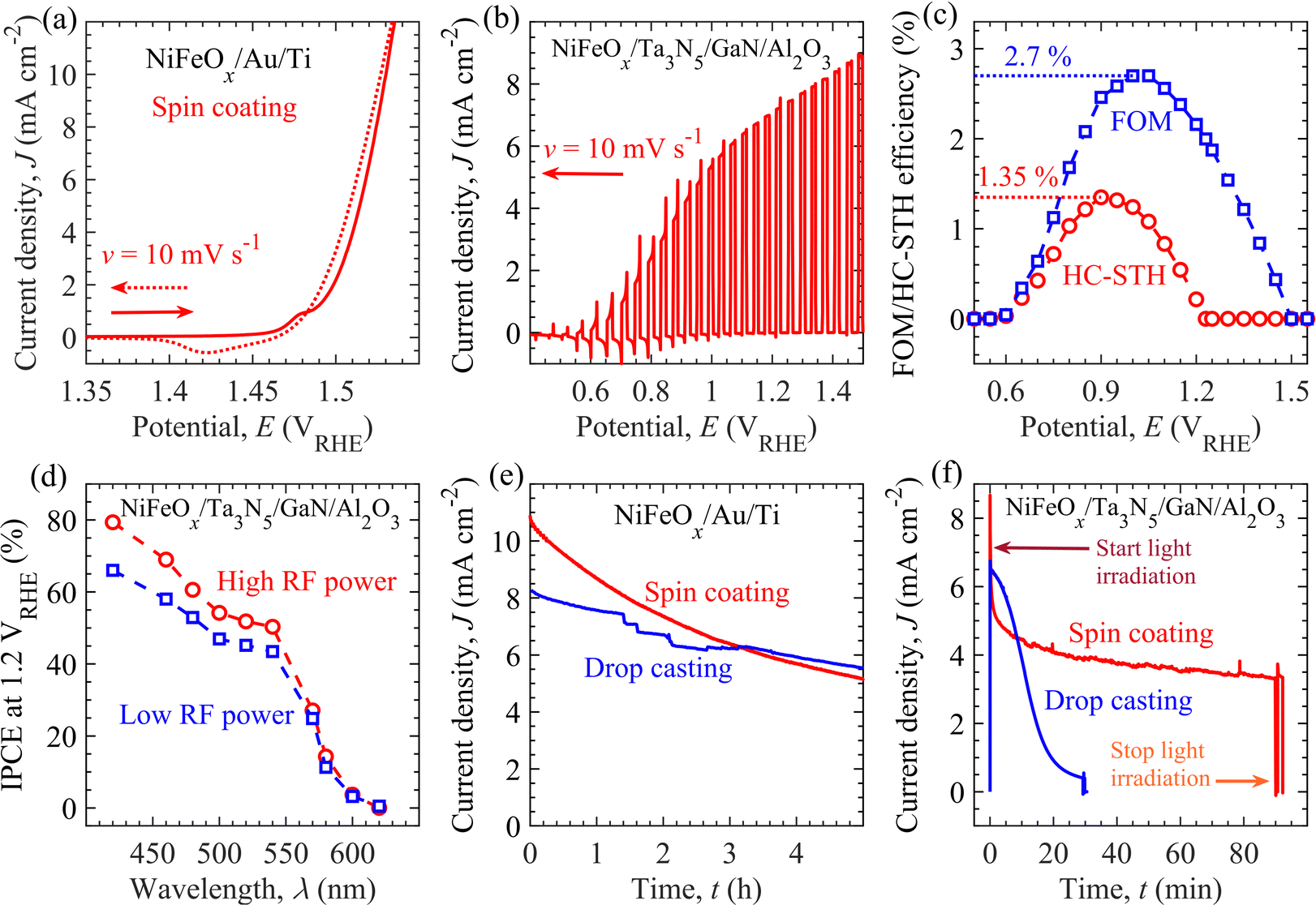 | ||
| Fig. 3 Photoelectrochemical features of Ta3N5 photoanode. (a) CV of NiFeOx/Au/Ti electrode, prepared by spin-coating method, at potential scan rate v (10 mV s−1) under dark condition. (b) J–E curve of NiFeOx/Ta3N5/GaN/Al2O3 semitransparent photoanode, prepared by spin-coating method, under chopped simulated AM1.5G solar illumination. (c) HC-STH energy conversion efficiency and FOM as a function of photoanode potential. (d) IPCE spectra of photoanodes (red: prepared by high-input-power RF-MS; blue: prepared by low-input-power RF-MS). (e) Chronoamperograms for NiFeOx/Au/Ti electrode at the electrode potential of 1.5 VRHE under dark condition (red: NiFeOx prepared by spin-coating; blue: NiFeOx prepared by drop-casting). (f) Evolution of current density of photoanodes at potential of 1.23 VRHE with time t (red: from spin-coating method, blue: drop-casting method) under continuous AM1.5G solar illumination. The measurements were performed in 1 M KOH aqueous solution with pH 13.8. The current density in (b and f) was obtained by normalizing the measured current (in three-electrode configuration) with the photoactive area (0.84 cm2 – spin coating; 0.86 cm2 – drop casting) of photoanodes, prepared by high-input-power RF-MS system. | ||
The PEC properties of the semitransparent NiFeOx/Ta3N5/GaN/Al2O3 photoanode include onset potential, photocurrent density at the standard water redox potential (1.23 VRHE) for OER activity, and water-splitting efficiency, were assessed under simulated AM1.5G solar illumination. The measurements were performed using a three-electrode configuration, as shown in Fig. S10 of ESI.† The PEC properties of Ta3N5 film with thicknesses ranging from 100 nm to 1000 nm were evaluated. The optimized Ta3N5 thickness of 800 nm produces a high photocurrent of ∼7.4 mA cm−2 at 1.23 VRHE (see Fig. S11, ESI†). Fig. 3b shows the photocurrent density (J)–potential (E) (J–E) curve of optimized NiFeOx/Ta3N5/GaN/Al2O3 semitransparent photoanode, prepared by spin-coating method, measured in a 1 M KOH aqueous solution with pH 13.8. A photocurrent of over 0.1 mA cm−2 is observed at a photoanode potential of more than 0.60 VRHE. We called this potential the onset potential Eon of the photoanode for the OER activity. From Fig. 3(a) and (b), the difference in the onset potential (ΔEon) of the NiFeOx/Au/Ti electrode (1.48 VRHE) and NiFeOx/Ta3N5/GaN/Al2O3 photoanode (0.60 VRHE) is 0.88 V. ΔEon indicates that the photogenerated charge carriers inside the Ta3N5 layers reduce the applied potential required to initiate the OER activity. The onset potential of the fabricated photoanode is close to the previously reported NiFeOx-modified Ta3N5 photoanodes prepared on the Ta,47 GaN/Al2O3,57 and quartz substrates.26,59 On the other hand, we observed a cathodic (or negative) shift of the onset potential compared to the communicated single metal oxide-based electrocatalyst (such as CoPi, CoOx, NiOx, and FeOx) loaded Ta3N5 photoanodes.47,65–67 In the literature, the onset potential of the Ta3N5-based photoanodes ranges from 0.5 VRHE to 0.8 VRHE, irrespective of preparation procedure, substrates, cation-doping, and electrocatalysts.47,50,53,59 Although the void-free Ta3N5 thin film is successfully developed herein, the Fermi-energy level pinning effect caused by surface (oxygen impurity and/or nitrogen-vacancy) defect states may limit the realized onset potential of NiFeOx/Ta3N5/GaN/Al2O3 photoanodes.46 Besides, the photocurrent density J rises with increasing applied potential E and reaches ∼7.4 mA cm−2 at 1.23 VRHE. As shown in Fig. S12 of ESI,† the NiFeOx/Ta3N5/GaN/Al2O3 photoanodes exhibit a reproducible photocurrent density of more than 7 mA cm−2 at 1.23 VRHE. Although the photocurrent varies slightly from sample to sample, an average photocurrent density of 7.37 ± 0.06 mA cm−2 at 1.23 VRHE is realized from five different Ta3N5-based photoanode samples. The realized photocurrent at 1.23 VRHE is 60% of the theoretical current limit of 12.4 mA cm−2 of Ta3N5 (for bandgap energy of 2.1 eV) at an external quantum efficiency of 100%.25 The photoanode prepared by high-input-power RF-MS exhibits an enhanced photocurrent density of 1.1 mA cm−2 at 1.23 VRHE compared to the photoanode developed with a conventional low-input-power RF-MS system (70 W).57 Compared to the spin-coated NiFeOx electrocatalyst, the drop-casting modification of the Ta3N5 surface leads to similar current potential features (e.g., 7.3 mA cm−2 at 1.23 VRHE; see Fig. S13, ESI†).
Fig. S14 of the ESI† presents the PEC characterization of NiFeOx/Ta3N5/GaN/Al2O3 photoanodes prepared by high (optimized) and low- (non-optimized) input-power RF-MS techniques. The optimized Ta3N5 photoanode exhibits larger photocurrents than non-optimized Ta3N5 photoanode in absence and presence of hole scavenger (H2O2) (Fig. S14(a) and (b), ESI†). The J–E curves for Ta3N5 photoanodes, acquired in electrolyte containing H2O2, facilitate the estimation the charge injection and charge separation efficiencies of photoanodes, in accordance with the previous reports.7 The charge injection efficiency (Fig. S14c, ESI†) of optimized photoanode is higher (∼80% at 0.9 VRHE) than that of non-optimized sample (∼60% at 1.0 VRHE). Similarly, the charge separation efficiency (Fig. S14d, ESI†) of optimized photoanode is higher than that of non-optimized photoanode. Besides this, in Fig. S14e of ESI,† the Nyquist plots under AM1.5G illumination at potential of 1.23 VRHE indicate relatively low charge transfer resistance (for hole transfer from Ta3N5 surface to electrolyte) of optimized photoanode as compared to non-optimized sample. These results suggest enhanced bulk and surface properties of optimized Ta3N5 to suppress recombination of charge carriers for efficient extraction of holes for OER activity. From Mott-Schottky analysis in Fig. S14f of ESI,† the flat band potential of optimized and non-optimized photoanodes are 0.19 VRHE and 0.31 VRHE, respectively.
Fig. 3c presents the half-cell solar-to-hydrogen (HC-STH) energy conversion efficiency and ratio-metric power-saved figure of merit (FOM) at various applied potentials of the NiFeOx/Ta3N5/GaN/Al2O3 photoanode. A schematic illustration and governing equations for evaluating the above performance metrics are provided in Fig. S15 in the ESI† and Materials and methods section (in ESI†), respectively. The maximum HC-STH efficiency and FOM are 1.35% at 0.9 VRHE and 2.7% at 1.0 VRHE, respectively. A significant improvement in the maximum HC-STH energy conversion efficiency is observed in comparison to the previously reported NiFeOx/Ta3N5/GaN/Al2O3 photoanode (1.15% at 0.94 VRHE)57 and CoOx-loaded Ta3N5/Ta photoanode (1.0% at 1.0 VRHE).47
Fig. 3d unveils photoanodes' incident-photon-to-current efficiency (IPCE) at 1.2 VRHE for different wavelengths of incident monochromatic light. The NiFeOx/Ta3N5/GaN/Al2O3 photoanodes generated an anodic current in response to light absorption at wavelengths less than 600 nm. The onset of the photocurrent response with the decrease in the wavelength is often called the light absorption edge (∼600 nm), which agrees with the reported Ta3N5 literature value.42 Tauc plot (derived from IPCE spectra) determines the bandgap energy of 2.06 eV (Fig. S16 in the ESI†). The IPCEs of the fabricated photoanode through the high-input-RF power are higher than the sample produced by low-input-power RF-MS.57 The enhanced IPCE spectra is consistent with the improved photocurrent density (by 1.1 mA cm−2) of the photoanodes,57 developed by high-input-power RF-MS (in Fig. 3b). In addition, the IPCEs increased with a decrease in wavelength. Light absorption at short wavelengths (e.g., 420 nm) produces charge carriers that are relatively closer to the surface than long wavelengths (500 nm). The photogenerated holes either diffused to the Ta3N5 surface for OER activity or were annihilated via recombination in the bulk of Ta3N5. The qualitative description of charge carrier transport suggests that charge carriers closer to the surface are less likely to recombine than more distant charges, resulting in the observed IPCE spectra.
The stability of the Ta3N5-based photoanode is critical and could depend on the durability of the NiFeOx electrocatalyst during OER activity. To investigate the durability of NiFeOx, NiFeOx was loaded over the Au/Ti electrodes by drop-casting or spin-coating. Fig. 3e shows the chronoamperograms of the light-insensitive NiFeOx/Au/Ti electrodes. These measurements were performed in a 1 M KOH aqueous solution with a pH of 13.9. With NiFeOx/Au/Ti electrodes, the electrode potential was modulated from 0.9 to 1.5 VRHE at an initial time t = 0 h to produce OER activity at the anodic current density of 10.9 mA cm−2 and 8.3 mA cm−2 from spin-coating and drop-casting methods, respectively. The current densities generated by both electrodes gradually decreased to 5 mA cm−2 after 5 h of electrochemical operation. The degradation in the current could originate from the loss of OER-active Fe species, which dissolve into the electrolyte solution as the most likely FeO42− species.68–70 Compared to the NiFeOx-loaded surface with the drop-casting method, the rate of current density degradation is higher for the NiFeOx-loaded surface with the spin-coating method owing to the larger dissolution of Fe species driven by high current density levels. The fraction of the NiFeOx-loaded surface retaining the OER-active Fe species f(t) decreases with time t as follows:
 | (1) |
Using similar deposition techniques and conditions, the electrocatalyst was loaded to develop NiFeOx/Ta3N5/GaN/Al2O3 photoanodes, and their impact on the durability of light-induced OER activity was investigated. As mentioned in Fig. 2, the uniform and non-uniform distributions of NiFeOx on the Ta3N5 surface were detected by spin-coating and drop-casting method, respectively. With a high-quality (void-free) Ta3N5 thin film, Fig. 3f exhibits the impact of electrocatalyst deposition methods on the photocurrent density's time (t) evolution at 1.23 VRHE on NiFeOx/Ta3N5/GaN/Al2O3 photoanodes under simulated AM1.5G solar illumination. The initial J (at t = 0 min) for the Ta3N5/GaN/Al2O3 sample with low (or non-uniform) coverage by NiFeOx (drop-casting method) was lower than that of the Ta3N5/GaN/Al2O3 specimen with high (or uniform) NiFeOx coverage (spin-coating method). The photocurrents herein are consistent with the observations from the J–E curves in Fig. 3b and Fig. S13 in ESI.† During the first 5 min of operation, a rapid decrease in photocurrent with time is characterized by high surface electrocatalyst coverage compared to that of low-surface-coverage-based samples. However, the high surface coverage photoanode achieved a stabilized photocurrent of 3.8 mA cm−2 after 80 min. In contrast, the photocurrent of the photoanode with low surface coverage decayed rapidly within 30 min of the photoelectrode operation. This improved stability of Ta3N5-based photoanode displays the crucial impact of (uniform vs. non-uniform) surface protection by NiFeOx.
These results demonstrate the correlation between the photoanodes' durability, electrocatalyst's intrinsic stability, and surface modification of Ta3N5 with an electrocatalyst. For instance, the deposition method did not significantly affect the overall intrinsic stability (Fig. 3e) of the electrocatalyst for up to 5 h. However, the electrocatalyst's high coverage (uniform) of the Ta3N5 surface showed enhanced photocurrent stability of up to 80 min, whereas the low surface coverage led to a rapid photocurrent decay within 30 min (Fig. 3f). This contrasting evolution of J with t indicates that an additional process could be involved in the J degradation of the photoanodes. In order to understand the real degradation mechanism of Ta3N5 photoanode towards OER activity, we performed the PEC measurement of bare-Ta3N5/GaN/Al2O3 photoanode under AM1.5G solar illumination. Before stability test, the bare Ta3N5 photoanode exhibits anodic photocurrent at applied potentials beyond onset potential of 1.1 VRHE, which reaches to ∼0.16 mA cm−2 at applied potential of 1.23 VRHE (Fig. S18a in red line, ESI†). However, the photocurrent of bare Ta3N5 photoanode ceases to exist within few minutes of continuous water splitting operation (Fig. S18(a) and (b), ESI†). X-ray photoelectron spectroscopy (XPS) analysis revealed the formation of TaOx and nitrogen vacancies after the stability test of the photoanodes (Fig. S19, ESI†). The Ta 4f peak shifted to a higher binding energy after the stability tests. In addition, the peaks of Ta 4f, N 1s, and O 1s in the XPS spectra can be observed at lower binding energy after continuous Ar etching (Fig. S20, ESI†), indicative of the removal of the TaOx layer on the Ta3N5 surface via surface etching. The shift of the Ta 4f peaks towards lower binding energies is most likely due to the Fermi level pinning of Ta3N5.46 These XPS observations indicate that the insulating TaOx layer is created at the Ta3N5/electrolyte interface with continuous OER activity. Thus, the durability of the NiFeOx/Ta3N5/GaN/Al2O3 photoanodes was influenced by NiFeOx dissolution and insulating TaOx formation. Increasing the loading amount or thickness of NiFeOx electrocatalyst could improve the durability of Ta3N5 photoanode for OER activity. However, the NiFeOx loading amount suppresses the light absorption inside Ta3N5 layer as well as decreases the light transmittance (essential to power the bottom CuInSe2 solar cells) at wavelengths longer than 600 nm (evident from Fig. S21, ESI†). Owing to such limitation on optical properties, the NiFeOx loading amount could not be increased beyond a certain threshold value for the improvement of durability along with the current density at 1.23 VRHE. Nevertheless, the stability of the Ta3N5-based photoanode is improved with uniform surface modification by electrocatalyst coating compared to a previous report (where the OER activity ceases to exist beyond 15 min).57
2.3. Application of Ta3N5 photoanodes for bias-free solar water splitting
Fig. 4a shows a schematic of the PEC–PV tandem cell. The tandem cell is composed of serially connected NiFeOx/Ta3N5/GaN/Al2O3 photoanode (top), dual-CuInSe2 (CIS)-based PV elements (behind the photoanode), and Pt/Ni electrodes. An ITO-carbon conductor housing connects the individual elements of the tandem cell. Under simulated AM1.5G solar illumination, photogenerated holes from the Ta3N5 film were utilized for OER activity, whereas the GaN layer extracted electrons. These extracted electrons recombine with the holes produced inside the CIS elements; however, the light-generated electrons of the CIS elements reach the Pt/Ni electrode for HER activity. Details of CIS-based PV elements including J–V characteristics are given in the Materials and methods section and Fig. S22 of the ESI.† Hence, in Fig. 4b, the tandem cell operates with the matched photocurrent (from photoanode and CIS-based PV elements) close to 7.3 mA cm−2 at the 1.2 VRHE. Considering a faradaic efficiency of 98%,57 the Ta3N5-CIS tandem device drives bias-free solar water splitting with an STH energy conversion efficiency of 9%, which is higher than that of metal oxide/nitride-based tandem cells (see Table S1 and Fig. S2 of ESI†). Besides photocatalytic (metal oxide/nitride) materials-based PEC–PV tandem systems, the PV grade materials-based wireless multijunction and PEC–PV tandem devices reached state-of-the-art STH efficiency up to ∼20% and durability up to 100 h (see Tables S2 and S3 of ESI†). However, the practical application of PV materials-based tandem systems could be limited or hindered due to high fabrication cost of multijunction and presence of unhealthy lead content in PEC–PV systems.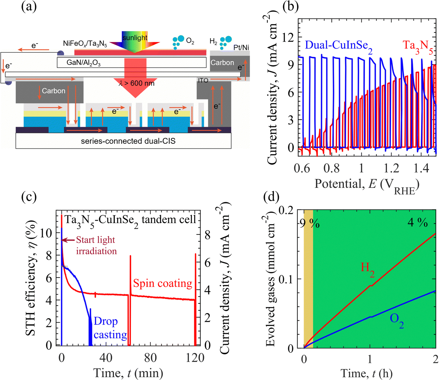 | ||
| Fig. 4 Bias-free overall solar water splitting from Ta3N5-CuInSe2-based tandem device. (a) Schematic diagram of a tandem cell, composed of NiFeOx/Ta3N5/GaN/Al2O3 photoanode, dual-CuInSe2 PV cells, and Pt/Ni electrode. (b) J–E curves of Ta3N5 photoanode (in front) and dual-CuInSe2 PV cells (behind photoanode) with respective photoactive area of 0.84 cm2 and 0.80 cm2. (c) Time evolution of STH energy conversion efficiency (left axis) and current density J (right axis) of the tandem cell. Here, J is determined by the ratio of current to photoactive area of Ta3N5 photoanodes. The Ta3N5 surface is loaded with high (red) and low (blue) coverage of NiFeOx with photoactive area of 0.84 cm2 and 0.86 cm2, respectively. (d) Evaluated evolution of hydrogen and oxygen gases, based on charge flow in panel (c) and faradaic efficiency of 98%. | ||
Fig. 4c shows the time evolution of the STH energy conversion efficiency of the tandem device. Although a spike-like (from capacitive response) photocurrent was initially observed, the non-faradaic process was expected to last a few seconds. For the photoanode surface modified by spin-coating method, the STH energy conversion efficiency of the tandem cell is about 9% after 0.25 min, which is maintained at more than 7% for 2 min. However, the tandem device based on the photoanode modified by the drop-casting method exhibited a relatively low STH energy conversion efficiency of 8% and durability for 1 min for efficiency beyond 7%. In Fig. 4d, the tandem cell with a high surface coverage photoanode displays relatively long-term durability of over 2 h to maintain the STH energy conversion efficiency above 4%. On the other hand, the STH energy conversion efficiency decayed rapidly to 4% within 20 min from a tandem device with a low-surface-coverage photoanode. These results demonstrate that the high coverage of the Ta3N5 surface by the NiFeOx electrocatalyst could extend the durability of overall solar water splitting. The effect of the electrocatalyst surface coverage on the durability of the tandem device was consistent with the stability test of NiFeOx/Au/Ti electrodes and Ta3N5-based photoanodes. Therefore, the tandem PEC cell durability test results demonstrated that the electrochemical characteristics of the electrocatalyst loaded on the photoelectrode surface affect the PEC properties of the photoelectrodes. To achieve efficient water splitting in the PEC water-splitting system, we show that the semiconductor properties of the photoelectrode materials and the electrocatalytic properties of the electrocatalyst, which functions as a surface modification layer, can be simultaneously evaluated, and that the PEC water-splitting rate can be significantly improved by designing a sophisticated solid/liquid interface.
2.4. Charge carrier dynamics of Ta3N5 thin film
The performance metrics of the photoanode, and hence the tandem cell, are generally limited by the recombination and/or trapping of photogenerated charge carriers inside the Ta3N5 thin film in addition to charge transfer to the electrolyte via NiFeOx. Accessing these properties is crucial for determining the governing material parameters and developing design guidelines for the performance enhancement of photoanode/tandem cells. For this, TAS measurements of the Ta3N5/GaN/Al2O3 sample (fabricated by high-input-power RF-MS) were performed to probe the dynamics of the absorption signal S(t) decay in the picosecond to microsecond time t range. The details of the TAS measurements are incorporated in the ESI.† The sample was excited by a pump photon energy of 3.1 eV to produce charge carriers inside a light penetration depth of 34 nm (∼1/αa; αa = 2.91 × 105 cm−1 is the absorption coefficient) at various pump fluence intensities PFL (0.075 to 4.5 μJ per pulse). According to the Lambert-Beer law, the initial density of the photogenerated charge carriers Δn0 = 1.88 × 1020 cm−3 at PFL = 3 μJ. These hot charge carriers relax rapidly in the femtoseconds to sub-picoseconds time scale by intraband relaxation processes and accumulate at the edge of valence and conduction bands.71–73 After intraband relaxation, the decay response of charge carriers is captured with a probe photon energy of 0.24 eV, and the resultant time evolution of S(t) was measured for different PFL.Fig. 5 unravels the dominant relaxation of the charge carriers behind the measured TAS characteristics of the Ta3N5 thin film. In Fig. 5a, the integrated photoluminescence (PL) spectrum and Tauc plot of the absorption coefficient (αa) spectrum show a bandgap energy of ∼2.1 eV. In addition, from Fig. 5b, the results indicate that the decay rate of S(t) increases with an increase in PFL, a typical bimolecular recombination feature of charge carriers. Moreover, the maximum absorption signal Sm (t ∼ 0.4 ps) increases almost linearly with an increase in PFL, photon density Ip, or Δn0 (Fig. S23 of ESI†), i.e., Sm = βΔn0, where β is the proportionality constant. Additionally, S(t) exhibits the power-law decay S(t) = At−α in the nanosecond to microsecond time range for various PFL, where A is the amplitude and α is the exponent. For n-type doped Y2Ti2O5S2 photocatalyst, the power-law absorption decay features in the sub- microsecond time range were attributed to the detrapping of holes from shallow exponential tail trap states of the valence band.74 From Hall effect measurements, the n-type doping density (nd) of the Ta3N5 thin film is significantly high (1.01 × 1020 cm−3). Following the Fermi-Dirac statistics, such a high nd leads to a Fermi-level energy close to the minimum energy of the conduction band and consequently fills the shallow trap states (if present) in the vicinity of the conduction band minimum. However, the shallow defect states near the valence band maximum can contribute to trapping/detrapping of holes. Considering these arguments, Fig. 5c presents the proposed numerical model to encapsulate dominant relaxation processes, such as bimolecular recombination of mobile charge carriers and trapping and detrapping of holes via exponential tail trap states of the valence band. The theoretical model formulations are included in the ESI.† As derived previously,74 the dynamics of the trapped hole density govern the power-law decay (S(t) = At−α) and is given by
| pAt(t) = Ntπα/([1 + nd/Δn0]Γ(1 − α)sin(πα)(ktNvt)α). | (2) |
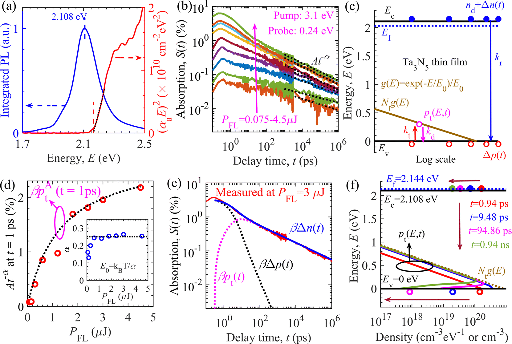 | ||
| Fig. 5 Charge carrier dynamics of Ta3N5 thin film. (a) Normalized integrated PL spectrum (left axis) between −0.1 ns and 0.7 ns obtained from picosecond time-resolved PL measurements for laser excitation of 3.1 eV, and Tauc plot (right axis) of absorption coefficient (αa) spectrum. (b) Absorption signal S(t) decay characteristics with time t at pump and probe photon energy of 3.1 eV and 0.24 eV, respectively. The S(t) follows power-law decay At−α (dotted lines) after around ten ns, where A and α is defined as the amplitude and exponent, respectively. (c) Proposed numerical model with band-to-band charge carrier recombination, trapping and detrapping of holes from exponential tail trap states Ntg(E). The detail of model description is provided in ESI.† (d) At−α (at t = 1 ps) and exponent α (inset) at various PFL. The dotted line represents βpAt (at t = 1 ps), where β and pAt corresponds to the proportionality constant and analytical trapped hole density pAt expressed by eqn (2), respectively. The dotted line in inset is a guide to eyes. (e) Time evolution of S(t) measured at PFL = 3 μJ (red line) and simulated density of trapped holes pt(t) (pink dotted line), mobile electrons Δn(t) (blue line) and holes Δp(t) (black dotted line). (f) Mapping of trapped holes pt(E, t) at energy E in cm−3 eV−1, Δn(t) (solid circles) and Δp(t) (open circles) in cm−3 at various time t for PFL = 3 μJ. | ||
The theoretical analysis of the TAS measurements determined various essential material parameters of the Ta3N5 thin film, as summarized in Table S4 in the ESI.† For instance, the evaluated nd = 8 × 1019 cm−3 corroborates well with the Hall effect measurements (1.01 × 1020 cm−3), whereas the quantified recombination rate constant kr (= 10−9 cm3 s−1) is close to the typical values of direct-bandgap semiconductors such as GaAs and lead halide perovskites. With carrier generation under AM1.5G solar illumination (i.e., Δn0 < nd), the evaluated carrier lifetime (krnd)−1 for recombination was only 12.5 ps. Moreover, the exponential tail trap states exhibit E0 = 104 meV, Nt = 9 × 1019 cm−3 and kt = 2 × 10⁻⁹ cm3 s−1. Such shallow trap states can additionally influence effective carrier lifetime and mobility.
2.5. Optoelectrical simulations of the Ta3N5 photoanode
Optoelectrical numerical modeling was employed to decipher the parameters governing the J–E characteristics of the fabricated NiFeOx/Ta3N5/GaN/Al2O3 semitransparent photoanode. Previously, optoelectrical modeling was utilized to study a wide range of solar energy harvesting materials and devices.75–78Fig. 6 shows the model calibration through optical and electrical simulations with the experimental data to extract performance-limiting parameters for the fabricated photoanode. Optical simulations using the complex refractive index shown in Fig. S25 in the ESI† revealed that the simulated light absorption below and transmission above the absorption edge (600 nm), shown in Fig. 6a, are in the range of 70–80%. Shorter wavelength sunlight is absorbed close to the solid/liquid interface; however, longer-wavelength sunlight penetrates deeper into the Ta3N5 thin film to generate charge carriers. The comparison of light absorption (Fig. 6a) and IPCE (Fig. 3d) suggests that the photogenerated charge carriers close to the electrolyte interface are extracted efficiently. In contrast, a significant fraction of charge carriers penetrating the Ta3N5 thin film are lost by recombination, leading to inefficient charge extraction. | ||
| Fig. 6 Optoelectrical simulation of the semitransparent Ta3N5 thin film-based photoanode. (a) Simulated light transmission (TR), reflection (RF) and absorption (Abs). (b) Fraction of AM1.5G solar spectrum (shaded gray area), absorbed (Abs × AM1.5G, shaded green area), and harvested (IPCE × AM1.5G, shaded blue area) along with the respective integrated current denisty. (c) The generation rate of charge carriers G with position x across Ta3N5 thin film (green line), evaluated using eqn (S16) (of ESI†). Here, q (∼1.602 × 10⁻¹⁹ C) is the elementary charge. (d) Simulated trend of current density at 1.23 VRHE against hole diffusion length Ldh. The shaded area is the regime around the measured current density of 7 mA cm−2. (e) Measured (in red) and simulated (blue line) J–E characteristics. (f) Energy band diagram and charge carrier generation (G)/recombination rate (R) with position x across Ta3N5 thin film corresponding to current density 7 mA cm−2 at 1.23 VRHE. Model calibration to the experimental data enables the estimation of performance-limiting parameters of the fabricated Ta3N5 photoanode. Ec, Ev, Fn, and Fp correspond to the energies of conduction band, valence band, quasi-Fermi-level for electrons and holes, respectively. | ||
Concerning the theoretical maximum current of 12.4 mA cm−2 for 2.1 eV, in Fig. 6b, the absorbed and harvested spectrum constitute an integrated current density of 9.27 and 7 mA cm−2, respectively, indicating that current densities of nearly 3.13 mA cm−2 and 2.27 mA cm−2 were lost through reflection and recombination in the fabricated photoanode, respectively. Fig. 6c presents the calculated charge carrier generation rate G across the thickness of Ta3N5 using the modified Lambert-Beer law (eqn (S16), ESI†) such that the integrated current density from G and the simulated absorption are equal. Using electrical simulations, Fig. 6d indicates that the current density at 1.23 VRHE decreases with the decrease in the hole diffusion length Ldh. In addition to optical loss, the current at 1.23 VRHE is lowered by bimolecular recombination at low Ldh. The mapping of the experimental current density range from 6.5 mA cm−2 to 8 mA cm−2 in Fig. 6d roughly estimates the Ldh in the range of 302 nm to 677 nm. The measured and simulated current density at 1.23 VRHE must be compared to obtain an initial estimate of Ldh. Fig. 6e suggests that the simulation agrees with the experimental J–E curve of the fabricated photoanode. This model calibration extracted performance-limiting parameters, as shown in Table S5 in the ESI.† We observe that the performance metrics such as the current density at 1.23 VRHE (Ja), fill factor (FF), and onset potential (Eon) are governed by parameters such as the minority hole diffusion length Ldh, hole extraction rate Sh from the Ta3N5 surface to the electrolyte, and parasitic series resistance Rs. Furthermore, in Fig. 6f, we provide the calculated energy band diagram and the generation and recombination rate of charge carriers under the operating condition with a current density of 7 mA cm−2 at 1.23 VRHE.
3. Conclusion
A highly efficient and durable NiFeOx/Ta3N5/GaN/Al2O3 semitransparent photoanode was established for a tandem cell configuration coupled with photovoltaics. A high-quality Ta3N5 thin film was fabricated using high-input-power radio-frequency magnetron sputtering (RF-MS), resulting in dense, void-free deposition of metallic Ta as an excellent precursor. With a Ta3N5-based photoanode prepared by high-input-power RF-MS, we demonstrated a photocurrent density of ∼7.4 mA cm−2 at 1.23 V vs. a reversible hydrogen electrode (VRHE), which was higher than that of the photoanode created by conventional low-input-power RF-MS. Moreover, an almost stabilized current density of 4 mA cm−2 at 1.23 VRHE was observed for more than 1 h of OER. This durability was otherwise impossible to achieve, where the direct contact of bare Ta3N5 to the electrolyte was minimized by the spin coating of NiFeOx, forming a uniform layer that covers the Ta3N5 surface, in sharp contrast with the drop-casting coating forming NiFeOx islands. The optimized photoanode exhibited a maximum half-cell solar-to-hydrogen (HC-STH) energy conversion efficiency and ratio-metric power-saved figure of merit (FOM) of 1.4% at 0.9 VRHE and 2.7% at 1.0 VRHE, respectively. Finally, the developed photoanode was integrated with dual-CuInSe2 photovoltaic cells to construct a photoelectrochemical–photovoltaic tandem device for bias-free overall solar water splitting. This tandem cell achieved a STH efficiency of 9% at the initial stage of the reaction, which is the highest among previously reported metal oxide/nitride-based tandem devices. In addition, a stable STH efficiency of 4% was demonstrated for 2 h of device operation. Furthermore, various measurements and theoretical simulations were performed to decipher the charge carrier dynamics and determine the unknown material parameters (such as recombination/trapping rate constants, doping density, lifetime, etc.) of the fabricated Ta3N5-based photoanode. We believe that our work presents significant advancements toward developing narrow-bandgap semiconductors for eco-friendly, sustainable, and practical solar hydrogen production.Data availability
The data that support the findings of this work are available from the corresponding authors upon reasonable request.Author contributions
T. H. and H. N. designed the photoelectrode concept and performed the experiments related to the preparation of Ta3N5/GaN/Al2O3 photoanodes and Pt/Ni/dual-CuInSe2 electrode, PEC measurements, and data analysis. T. H., Y. K., and K. T. performed electrochemical measurements for NiFeOx electrocatalyst and data analysis. Y. P., Y. K., and Y. S. performed material characterization (SEM-EDS) and surface modification of Ta3N5/GaN/Al2O3 photoanode. V. N. and K. S. conducted the theoretical analysis and simulations. R. S. and H. M. performed TAS and PL measurements. M. N. and N. S. performed TEM and STEM observations and data analysis. K. D. planned and supervised this project. T. H., V. N., Y. P., K. S., and K. D. wrote the manuscript. All the authors contributed to the manuscript revisions.Conflicts of interest
The authors declare no competing interest.Acknowledgements
This work was financially supported by the Artificial Photo-synthesis Project of the New Energy and Industrial Technology Development Organization (NEDO). This work was also funded in part by Grant-in-Aid for Early-Career Scientists (No. 19K15670) from JSPS. A part of this work was conducted at the Advanced Characterization Nanotechnology Platform of the University of Tokyo, supported by the ‘‘Nanotechnology Platform’’ of the Ministry of Education, Culture, Sports, Science and Technology (MEXT), Japan (JPMXP09A-21-UT-0046). We would like to thank to the Solar Frontier company (https://www.solar-frontier.com/) for providing us CuInSe2 photovoltaic cells.References
- M. G. Walter, E. L. Warren, J. R. McKone, S. W. Boettcher, Q. Mi, E. A. Santori and N. S. Lewis, Chem. Rev., 2010, 110, 6446–6473 CrossRef CAS PubMed.
- J. R. McKone, N. S. Lewis and H. B. Gray, Chem. Mater., 2014, 26, 407–414 CrossRef CAS.
- J. Jia, L. C. Seitz, J. D. Benck, Y. Huo, Y. Chen, J. W. D. Ng, T. Bilir, J. S. Harris and T. F. Jaramillo, Nat. Commun., 2016, 7, 13237 CrossRef CAS PubMed.
- B. A. Pinaud, J. D. Benck, L. C. Seitz, A. J. Forman, Z. Chen, T. G. Deutsch, B. D. James, K. N. Baum, G. N. Baum, S. Ardo, H. Wang, E. Miller and T. F. Jaramillo, Energy Environ. Sci., 2013, 6, 1983–2002 RSC.
- M. R. Shaner, H. A. Atwater, N. S. Lewis and E. W. McFarland, Energy Environ. Sci., 2016, 9, 2354–2371 RSC.
- Y. Xiao, C. Feng, J. Fu, F. Wang, C. Li, V. F. Kunzelmann, C. M. Jiang, M. Nakabayashi, N. Shibata, I. D. Sharp, K. Domen and Y. Li, Nat. Catal., 2020, 3, 932–940 CrossRef CAS.
- Y. Pihosh, T. Minegishi, V. Nandal, T. Higashi, M. Katayama, T. Yamada, Y. Sasaki, K. Seki, Y. Suzuki, M. Nakabayashi, M. Sugiyama and K. Domen, Energy Environ. Sci., 2020, 13, 1519–1530 RSC.
- Y. Kawase, T. Higashi, K. Domen and K. Takanabe, Adv. Energy Sustainability Res., 2021, 2, 2100023 CrossRef.
- M. S. Prévot and K. Sivula, J. Phys. Chem. C, 2013, 117, 17879–17893 CrossRef.
- K. T. Fountaine, H. J. Lewerenz and H. A. Atwater, Nat. Commun., 2016, 7, 13706 CrossRef CAS PubMed.
- H. Song, S. Luo, H. Huang, B. Deng and J. Ye, ACS Energy Lett., 2022, 7, 1043–1065 CrossRef CAS.
- S. Hu, C. Xiang, S. Haussener, A. D. Berger and N. S. Lewis, Energy Environ. Sci., 2013, 6, 2984–2993 RSC.
- J. Brillet, J. H. Yum, M. Cornuz, T. Hisatomi, R. Solarska, J. Augustynski, M. Graetzel and K. Sivula, Nat. Photonics, 2012, 6, 824–828 CrossRef CAS.
- W. J. Lee, P. S. Shinde, G. H. Go and E. Ramasamy, Int. J. Hydrogen Energy, 2011, 36, 5262–5270 CrossRef CAS.
- Y. Pihosh, I. Turkevych, K. Mawatari, J. Uemura, Y. Kazoe, S. Kosar, K. Makita, T. Sugaya, T. Matsui, D. Fujita, M. Tosa, M. Kondo and T. Kitamori, Sci. Rep., 2015, 5, 11141 CrossRef PubMed.
- F. F. Abdi, L. Han, A. H. M. Smets, M. Zeman, B. Dam and R. van de Krol, Nat. Commun., 2013, 4, 2195 CrossRef PubMed.
- Y. Kuang, Q. Jia, G. Ma, T. Hisatomi, T. Minegishi, H. Nishiyama, M. Nakabayashi, N. Shibata, T. Yamada, A. Kudo and K. Domen, Nat. Energy, 2016, 2, 16191 CrossRef.
- Y. S. Chen, J. S. Manser and P. V. Kamat, J. Am. Chem. Soc., 2015, 137, 974–981 CrossRef CAS PubMed.
- Y. Pihosh, J. Uemura, I. Turkevych, K. Mawatari, Y. Kazoe, A. Smirnova and T. Kitamori, Angew. Chem., Int. Ed., 2017, 56, 8130–8133 CrossRef CAS PubMed.
- D. Huang, K. Wang, L. Li, K. Feng, N. An, S. Ikeda, Y. Kuang, Y. Ng and F. Jiang, Energy Environ. Sci., 2021, 14, 1480–1489 RSC.
- A. Duret and M. Grätzel, J. Phys. Chem. B, 2005, 109, 17184–17191 CrossRef CAS PubMed.
- J. W. Jang, C. Du, Y. Ye, Y. Lin, X. Yao, J. Thorne, E. Liu, G. McMahon, J. Zhu, A. Javey, J. Guo and D. Wang, Nat. Commun., 2015, 6, 7447 CrossRef PubMed.
- K. Y. Yoon, J. Park, M. Jung, S. G. Ji, H. Lee, J. H. Seo, M. J. Kwak, S. Il Seok, J. H. Lee and J. H. Jang, Nat. Commun., 2021, 12, 4309 CrossRef CAS PubMed.
- B. A. Pinaud, P. C. K. Vesborg and T. F. Jaramillo, J. Phys. Chem. C, 2012, 116, 15918–15924 CrossRef CAS.
- V. Nandal, Y. Pihosh, T. Higashi, T. Minegishi, T. Yamada, K. Seki, M. Sugiyama and K. Domen, Energy Environ. Sci., 2021, 14, 4038–4047 RSC.
- T. Higashi, H. Nishiyama, Y. Otsuka, Y. Kawase, Y. Sasaki, M. Nakabayashi, M. Katayama, T. Minegishi, N. Shibata, K. Takanabe, T. Yamada and K. Domen, ChemSusChem, 2020, 13, 1974–1978 CrossRef CAS PubMed.
- M. Kim, B. Lee, H. Ju, J. Y. Kim, J. Kim and S. W. Lee, Adv. Mater., 2019, 31, 1903316 CrossRef PubMed.
- S. Lee, L. Ji, A. C. De Palma and E. T. Yu, Nat. Commun., 2021, 12, 3982 CrossRef CAS PubMed.
- R. Fan, S. Cheng, G. Huang, Y. Wang, Y. Zhang, S. Vanka, G. A. Botton, Z. Mi and M. Shen, J. Mater. Chem. A, 2019, 7, 2200–2209 RSC.
- S. A. Lee, I. J. Park, J. W. Yang, J. Park, T. H. Lee, C. Kim, J. Moon, J. Y. Kim and H. W. Jang, Cell Reports Phys. Sci., 2020, 1, 100219 CrossRef CAS.
- J. H. Kim, H. E. Kim, J. H. Kim and J. S. Lee, J. Mater. Chem. A, 2020, 8, 9447–9482 RSC.
- H. Kobayashi, N. Sato, M. Orita, Y. Kuang, H. Kaneko, T. Minegishi, T. Yamada and K. Domen, Energy Environ. Sci., 2018, 11, 3003–3009 RSC.
- J. Luo, Z. Li, S. Nishiwaki, M. Schreier, M. T. Mayer, P. Cendula, Y. H. Lee, K. Fu, A. Cao, M. K. Nazeeruddin, Y. E. Romanyuk, S. Buecheler, S. D. Tilley, L. H. Wong, A. N. Tiwari and M. Grätzel, Adv. Energy Mater., 2015, 5, 1501520 CrossRef.
- H. Kaneko, T. Minegishi, M. Nakabayashi, N. Shibata, Y. Kuang, T. Yamada and K. Domen, Adv. Funct. Mater., 2016, 26, 4570–4577 CrossRef CAS.
- S. K. Karuturi, H. Shen, A. Sharma, F. J. Beck, P. Varadhan, T. Duong, P. R. Narangari, D. Zhang, Y. Wan, J. H. He, H. H. Tan, C. Jagadish and K. Catchpole, Adv. Energy Mater., 2020, 10, 2000772 CrossRef CAS.
- D. Xue, M. Kan, X. Qian and Y. Zhao, ACS Sustainable Chem. Eng., 2018, 6, 16228–16234 CrossRef CAS.
- S. Wang, P. Chen, Y. Bai, J. H. Yun, G. Liu and L. Wang, Adv. Mater., 2018, 30, 1800486 CrossRef PubMed.
- D. Gurudayal, M. H. Sabba, L. H. Kumar, J. Wong, M. Barber, M. Grätzel and N. Mathews, Nano Lett., 2015, 15, 3833–3839 CrossRef CAS PubMed.
- Gurudayal, R. A. John, P. P. Boix, C. Yi, C. Shi, M. C. Scott, S. A. Veldhuis, A. M. Minor, S. M. Zakeeruddin, L. H. Wong, M. Grätzel and N. Mathews, ChemSusChem, 2017, 10, 2449–2456 CrossRef CAS PubMed.
- J. Park, K. Y. Yoon, T. Kim, H. Jang, M. J. Kwak, J. Y. Kim and J. H. Jang, Nano Energy, 2020, 76, 105089 CrossRef CAS.
- E. Nurlaela, M. Nakabayashi, Y. Kobayashi, N. Shibata, T. Yamada and K. Domen, Sustain. Energy Fuels, 2020, 4, 2293–2300 RSC.
- W. J. Chun, A. Ishikawa, H. Fujisawa, T. Takata, J. N. Kondo, M. Hara, M. Kawai, Y. Matsumoto and K. Domen, J. Phys. Chem. B, 2003, 107, 1798–1803 CrossRef CAS.
- G. Liu, S. Ye, P. Yan, F. Xiong, P. Fu, Z. Wang, Z. Chen, J. Shi and C. Li, Energy Environ. Sci., 2016, 9, 1327–1334 RSC.
- Z. Wang, Y. Inoue, T. Hisatomi, R. Ishikawa, Q. Wang, T. Takata, S. Chen, N. Shibata, Y. Ikuhara and K. Domen, Nat. Catal., 2018, 1, 756–763 CrossRef CAS.
- Q. Wang, T. Hisatomi, S. S. K. Ma, Y. Li and K. Domen, Chem. Mater., 2014, 26, 4144–4150 CrossRef CAS.
- Y. He, J. E. Thorne, C. H. Wu, P. Ma, C. Du, Q. Dong, J. Guo and D. Wang, Chem, 2016, 1, 640–655 CAS.
- M. Zhong, T. Hisatomi, Y. Sasaki, S. Suzuki, K. Teshima, M. Nakabayashi, N. Shibata, H. Nishiyama, M. Katayama, T. Yamada and K. Domen, Angew. Chem., Int. Ed., 2017, 56, 4739–4743 CrossRef CAS PubMed.
- J. Fu, Z. Fan, M. Nakabayashi, H. Ju, N. Pastukhova, Y. Xiao, C. Feng, N. Shibata, K. Domen and Y. Li, Nat. Commun., 2022, 13, 729 CrossRef CAS PubMed.
- J. Liu, W. Luo, K. Zhu, X. Wen, F. Xiu, J. Yuan, Z. Zou and W. Huang, RSC Adv., 2017, 7, 30650–30656 RSC.
- J. Seo, T. Takata, M. Nakabayashi, T. Hisatomi, N. Shibata, T. Minegishi and K. Domen, J. Am. Chem. Soc., 2015, 137, 12780–12783 CrossRef CAS PubMed.
- L. Pei, B. Lv, S. Wang, Z. Yu, S. Yan, R. Abe and Z. Zou, ACS Appl. Energy Mater., 2018, 1, 4150–4157 CrossRef CAS.
- D. Akagi, Y. Kageshima, Y. Hashizume, S. Aoi, Y. Sasaki, H. Kaneko, T. Higashi, T. Hisatomi, M. Katayama, T. Minegishi, S. Noda and K. Domen, ChemPhotoChem, 2019, 3, 521–524 CrossRef CAS.
- Y. W. Kim, S. Cha, I. Kwak, I. S. Kwon, K. Park, C. S. Jung, E. H. Cha and J. Park, ACS Appl. Mater. Interfaces, 2017, 9, 36715–36722 CrossRef CAS PubMed.
- Y. Pihosh, V. Nandal, T. Minegishi, M. Katayama, T. Yamada, K. Seki, M. Sugiyama and K. Domen, ACS Energy Lett., 2020, 5, 2492–2497 CrossRef CAS.
- M. Higashi, K. Domen and R. Abe, Energy Environ. Sci., 2011, 4, 4138–4147 RSC.
- H. Hajibabaei, O. Zandi and T. W. Hamann, Chem. Sci., 2016, 7, 6760–6767 RSC.
- T. Higashi, H. Nishiyama, Y. Suzuki, Y. Sasaki, T. Hisatomi, M. Katayama, T. Minegishi, K. Seki, T. Yamada and K. Domen, Angew. Chem., Int. Ed., 2019, 58, 2300–2304 CrossRef CAS PubMed.
- H. Hajibabaei, D. J. Little, A. Pandey, D. Wang, Z. Mi and T. W. Hamann, ACS Appl. Mater. Interfaces, 2019, 11, 15457–15466 CrossRef CAS PubMed.
- Y. Kawase, T. Higashi, M. Katayama, K. Domen and K. Takanabe, ACS Appl. Mater. Interfaces, 2021, 13, 16317–16325 CrossRef CAS PubMed.
- N. Kaiser, Appl. Opt., 2002, 41, 3053–3060 CrossRef CAS PubMed.
- O. Kluth, G. Schöpe, J. Hüpkes, C. Agashe, J. Müller and B. Rech, Thin Solid Films, 2003, 442, 80–85 CrossRef CAS.
- E. Nurlaela, M. Harb, S. del Gobbo, M. Vashishta and K. Takanabe, J. Solid State Chem., 2015, 229, 219–227 CrossRef CAS.
- W. Zhang, X. Jiang, Z. Dong, J. Wang, N. Zhang, J. Liu, G. R. Xu and L. Wang, Adv. Funct. Mater., 2021, 31, 2107181 CrossRef CAS.
- C. C. L. McCrory, S. Jung, J. C. Peters and T. F. Jaramillo, J. Am. Chem. Soc., 2013, 135, 16977–16987 CrossRef CAS PubMed.
- M. Liao, J. Feng, W. Luo, Z. Wang, J. Zhang, Z. Li, T. Yu and Z. Zou, Adv. Funct. Mater., 2012, 22, 3066–3074 CrossRef CAS.
- Z. Wang, Y. Qi, C. Ding, D. Fan, G. Liu, Y. Zhao and C. Li, Chem. Sci., 2016, 7, 4391–4399 RSC.
- G. Liu, P. Fu, L. Zhou, P. Yan, C. Ding, J. Shi and C. Li, Chem. – Eur. J., 2015, 21, 9624–9628 CrossRef CAS PubMed.
- K. Obata and K. Takanabe, Angew. Chem., Int. Ed., 2018, 57, 1616–1620 CrossRef CAS PubMed.
- F. D. Speck, K. E. Dettelbach, R. S. Sherbo, D. A. Salvatore, A. Huang and C. P. Berlinguette, Chem, 2017, 2, 590–597 CAS.
- S. Zou, M. S. Burke, M. G. Kast, J. Fan, N. Danilovic and S. W. Boettcher, Chem. Mater., 2015, 27, 8011–8020 CrossRef CAS.
- M. Bernardi, D. Vigil-Fowler, C. S. Ong, J. B. Neaton and S. G. Louie, Proc. Natl. Acad. Sci. U. S. A., 2015, 112, 5291–5296 CrossRef CAS PubMed.
- A. D. Wright, C. Verdi, R. L. Milot, G. E. Eperon, M. A. Pérez-Osorio, H. J. Snaith, F. Giustino, M. B. Johnston and L. M. Herz, Nat. Commun., 2016, 7, 11755 CrossRef PubMed.
- M. Monti, S. X. Tao, M. Staniforth, A. Crocker, E. Griffin, A. Wijesekara, R. A. Hatton and J. Lloyd-Hughes, J. Phys. Chem. C, 2018, 122, 20669–20675 CrossRef CAS.
- V. Nandal, R. Shoji, H. Matsuzaki, A. Furube, L. Lin, T. Hisatomi, M. Kaneko, K. Yamashita, K. Domen and K. Seki, Nat. Commun., 2021, 12, 7055 CrossRef CAS PubMed.
- V. Nandal and P. R. Nair, J. Phys. Chem. C, 2018, 122, 27935–27940 CrossRef CAS.
- V. Nandal, Y. Suzuki, H. Kobayashi, K. Domen and K. Seki, J. Mater. Chem. A, 2020, 8, 9194–9201 RSC.
- S. Agarwal, V. Nandal, H. Yadav and K. Kumar, J. Appl. Phys., 2021, 129, 203101 CrossRef CAS.
- V. Nandal, S. Agarwal and P. R. Nair, Phys. Chem. Chem. Phys., 2021, 23, 24421–24427 RSC.
Footnote |
| † Electronic supplementary information (ESI) available. See DOI: https://doi.org/10.1039/d2ee02090d |
| This journal is © The Royal Society of Chemistry 2022 |