
 Open Access Article
 This Open Access Article is licensed under a Creative Commons Attribution-Non Commercial 3.0 Unported Licence
Elimination of light-induced degradation at the nickel oxide-perovskite heterojunction by aprotic sulfonium layers towards long-term operationally stable inverted perovskite solar cells†
Tianhao
Wu
a,
Luis K.
Ono
 a,
Rengo
Yoshioka
b,
Chenfeng
Ding
a,
Congyang
Zhang
a,
Silvia
Mariotti
a,
Jiahao
Zhang
a,
Kirill
Mitrofanov
b,
Xiao
Liu
c,
Hiroshi
Segawa
c,
Ryota
Kabe
b,
Liyuan
Han
cd and
Yabing
Qi
*a
a,
Rengo
Yoshioka
b,
Chenfeng
Ding
a,
Congyang
Zhang
a,
Silvia
Mariotti
a,
Jiahao
Zhang
a,
Kirill
Mitrofanov
b,
Xiao
Liu
c,
Hiroshi
Segawa
c,
Ryota
Kabe
b,
Liyuan
Han
cd and
Yabing
Qi
*a
aEnergy Materials and Surface Sciences Unit (EMSSU), Okinawa Institute of Science and Technology Graduate University (OIST), 1919-1 Tancha, Onna-son, Kunigami-gun, Okinawa 904-0495, Japan. E-mail: Yabing.Qi@OIST.jp
bOrganic Optoelectronics Unit, Okinawa Institute of Science and Technology Graduate University, 1919-1 Tancha, Onna-son, Kunigami-gun, Okinawa 904-0495, Japan
cSpecial Division of Environmental and Energy Science, Komaba Organization for Educational Excellence (KOMEX), College of Arts and Sciences, University of Tokyo, Tokyo 153-8902, Japan
dState Key Laboratory of Metal Matrix Composites, School of Material Science and Engineering, Shanghai Jiao Tong University, Shanghai 200240, China
First published on 23rd September 2022
Abstract
Nickel oxide (NiOx) is a promising hole-selective contact to produce efficient inverted p-i-n structured perovskite solar cells (PSCs) due to its high carrier mobility and high transparency. However, the light-induced degradation of the NiOx–perovskite heterojunction is the main factor limiting its long-term operational lifetime. In this study, we used the time-resolved mass spectrometry technique to clarify the degradation mechanism of the NiOx-formamidinium–methylammonium iodide perovskite (a common composition for high-performance PSCs) heterojunction under operational conditions, and observed that (1) oxidation of iodide and generation of free protons under 1-sun illumination, (2) formation of volatile hydrogen cyanide, methyliodide, and ammonia at elevated temperatures, and (3) a condensation reaction between the organic components under a high vapor pressure. To eliminate these multi-step photochemical reactions, we constructed an aprotic trimethylsulfonium bromide (TMSBr) buffer layer at the NiOx/perovskite interface, which enables excellent photo-thermal stability, a matched lattice parameter with the perovskite crystal, and robust trap-passivation ability. Inverted PSCs stabilized with the TMSBr buffer layer reached the maximum efficiency of 22.1% and retained 82.8% of the initial value after continuous operation for 2000 hours under AM1.5G light illumination, which translates into a T80 lifetime of 2310 hours that is among the highest operational lifetimes for NiOx-based PSCs.
Broader contextPerovskite solar cells (PSCs) have emerged as one of the most outstanding photovoltaic technologies, but the stability issue is still a major challenge for their commercial application. The inverted p-i-n device structure using the charge-selective contacts with less sensitivity to ambient conditions is regarded as a viable route to fabricate high-performance PSCs with better environmental stability, and nickel oxide (NiOx) is the most frequently used hole-selective contact at the illumination side due to its high carrier mobility, low cost, and high transparency. However, the operational lifetime of NiOx-based inverted PSCs is still relatively short (around 1000 hours), and their long-term operational stability is largely limited by the degradation at the NiOx–perovskite heterojunction under continuous 1-sun illumination. In this regard, a fundamental understanding of the degradation mechanism at the NiOx–perovskite heterojunction is urgently needed, and development of a simple strategy based on the construction of a photo-thermal stable buffer layer that can synergistically eliminate the light-induced degradation and minimize the charge recombination loss in NiOx-based inverted PSCs is highly desirable, which is promising to narrow their efficiency and stability gap compared with other mature photovoltaic technologies. |
Introduction
Perovskite solar cells (PSCs) developed rapidly as a promising photovoltaic technology due to the outstanding optoelectronic properties of organic metal halide perovskite materials, such as long carrier diffusion length, low cost, and solution processability.1–3 The power conversion efficiency (PCE) of PSCs has recently exceeded the record PCE value of copper indium gallium selenium solar cells and approached that of crystalline-Si solar cells,4 but the long-term operational stability is still a major bottleneck for PSC commercialization owing to the soft-material nature of perovskites and related interfaces.5,6 The inverted (p-i-n) devices are considered as a viable route toward efficient and stable PSCs under long-term light and thermal stresses. In general, dopant-free fullerene-based materials with good ambient stability are used as the electron-selective contact for inverted PSCs, while nickel oxide (NiOx) with high transparency and hole mobility is one of the most frequently used hole-selective contacts at the illumination side.7–9So far, NiOx-based inverted PSCs have exhibited the best-reported stability of 500–1000 hours under a variety of test conditions, including the 85 °C–85% damp heat test, the temperature cycling test (from −40 °C to 85 °C), and continuous operation under AM 1.5G light illumination and at elevated temperatures.10–14 On the other hand, recent studies revealed that the deprotonation and redox reactions between the organic iodide components in a perovskite absorber and Ni3+ in the NiOx layer led to a relatively low device efficiency and stability.12,15 Typically, Ni3+ is a p-type dopant for improving the hole mobility of the NiOx films and could be easily generated by doping monovalent cations (such as Li+, Ag+, and Cs+) or thermal annealing during the deposition processes, including spray-coating, atomic layer deposition, and sputtering.16–19 To further improve the PSC performance, excess organic iodide salts were added into the perovskite layer to compensate for the loss of components near the NiOx contact, which enables the device efficiency approaching 20% and over a 500-hour operational lifetime.12 Afterwards, the self-assembled monolayers such as MeO-2PACz, imidazolium derivatives, amine silane coupling agents, and trimethylolpropane were used to modify the NiOx surface for suppressing deprotonation and redox reactions,20–23 but the organic monolayers deposited on the device illumination side bring additional instability issues triggered by UV light for a long-term operation.24 In this regard, inorganic metallic halides including NaCl, KCl, and CsBr were chosen as the buffer layers between NiOx and perovskites, which enable an efficiency of over 21% and an operational lifetime of up to 1000 hours.25,26 Nevertheless, the size mismatch between alkali metal cations and A-site components may break the perovskite lattice and induce phase segregation under illumination, which limit the further improvement of operational lifetime.27 Moreover, the degradation mechanism at the NiOx–perovskite heterojunction under real operational conditions (1-sun illumination with elevated temperature) is still unclear, and development of in situ characterization techniques is urgently needed to identify the degradation products and further clarify the degradation dynamics.
To overcome the above-mentioned degradation issues, aprotic alkyl sulfoniums with a good photo-thermal stability and a similar cation size to the commonly used A-site cations in perovskites, formamidinium (FA+) and methylammonium (MA+), are a potential candidate to stabilize the NiOx–perovskite heterojunction. Falaras et al. first assembled the trimethylsulfonium (TMS+) cation into a perovskite lattice, and they found that the effective ionic radius of TMS+ (244 pm) is intermediate between those of MA+ (217 pm) and FA+ (253 pm) and much larger than that of Cs+ (167 pm),28 indicating a good size match with the mixed-cation FAMA-perovskite absorber that is widely used in high-performance PSCs. The TMSPbI3 perovskite film remained stable for more than 50 days under high-humidity conditions without any phase degradation attributed to the absence of hydrogen bonding interactions between TMS+ and water molecules, further confirming its aprotic nature.29 Other aprotic sulfoniums with a similar structure, such as trimethylsulfoxonium (TMSO+) and butyldimethylsulfonium (BDMS+), also exhibit a better photostability than the protic ammonium counterparts.30,31
In this work, we used the time-resolved quadrupole mass spectrometry (MS) technique to reveal the degradation mechanism of the NiOx-FAMAPbI3 perovskite heterojunction under the operational conditions, as depicted in Scheme 1: (1) generation of iodine vapor and free protons via the oxidation and deprotonation reactions; (2) formation of volatile products at elevated temperatures, including hydrogen cyanide (HCN), methyliodide (CH3I), and ammonia (NH3); (3) formation of a condensation product, N-methyl formamidine, with the increased vapor pressures of the dissociated FA and MA molecules. Inspired by the aprotic nature, good photo-thermal stability, suitable size of TMS+, and the high oxidation potential of bromine, we introduced a novel TMSBr buffer layer between NiOx and perovskite by the vapor-deposition method to eliminate these multi-step photochemical reactions. Theoretical calculations and experimental results showed that TMSBr could also retain the lattice coherence and minimize the trap density at the NiOx/perovskite interface. Consequently, the TMSBr-stabilized inverted PSCs (1.53 eV bandgap) exhibited a promising efficiency of 22.1% with an open-circuit voltage (VOC) of 1.18 V (and a VOC of 1.22 V for 1.66 eV bandgap PSCs) and could retain approximately 82.8% of the initial efficiency after 2000 hour operation under AM1.5G light illumination, which translates into an estimated T80 lifetime of 2310 hours (the time over which the efficiency reduces to 80% of its initial value), which is among the highest operational lifetimes reported for NiOx-based PSCs.
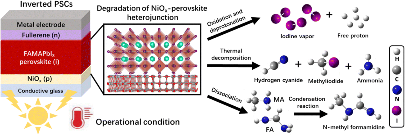 | ||
| Scheme 1 The degradation mechanism of the NiOx–perovskite heterojunction in inverted PSCs under operational conditions (1-sun illumination at elevated temperature) revealed by the time-resolved quadrupole MS findings. | ||
Results and discussion
First, we conducted density functional theory (DFT) calculations to visualize the difference in electronic properties between aprotic TMS+ and protic FA+ and MA+ cations. Fig. 1a shows the calculated electrostatic potential (ESP) of different cations. In the case of MA+, the positive charges (blue ESP region) were concentrated on the protons of the –NH3 group, which provides highly active sites for the deprotonation reaction. Similarly, the positive charges of FA+ were located at the reactive protons on both carbon and nitrogen atoms. By contrast, the positive charges of TMS+ located at the central S atom and the protons of the –CH3 group show a relatively neutral property, which significantly reduces the activity for deprotonation and decomposition reactions. Furthermore, the structure of TMSBr-terminated FAMAPbI3 perovskites on the NiO(001) substrate after a relaxation process based on the DFT method is depicted in Fig. 1a, and it can be found that the suitable effective radius of TMS+ between those of FA+ and MA+ keeps the corner-sharing octahedron ([PbI6]4−) perovskite lattice near the NiO(001) substrate, enabling a good electronic contact for carrier extraction (details of the DFT calculations can be found in the ESI†).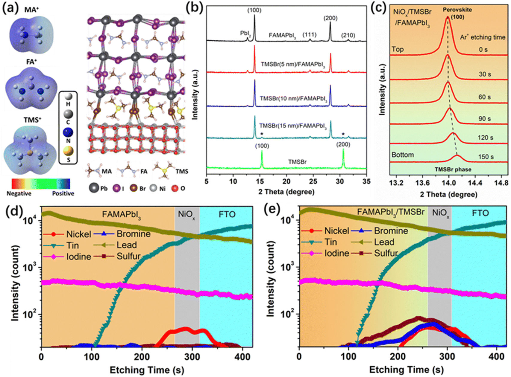 | ||
| Fig. 1 Aprotic TMSBr buffer layers introduced at the NiOx/perovskite interface. (a) Calculated ESP profiles of MA+, FA+, and TMS+ cations, and the geometry-optimized structure of TMSBr-terminated FAMAPbI3 perovskite on the NiO(001) substrate. (b) XRD patterns of the pure FAMAPbI3, the FAMAPbI3 with different thicknesses of TMSBr, and pure TMSBr films coated on the FTO/NiOx substrate. (c) Depth-dependent XRD patterns of the NiOx/TMSBr (10 nm)/FAMAPbI3 film at different Ar+ etching times. (d and e) SIMS profiles of the FAMAPbI3 perovskite films (d) without and (e) with the TMSBr buffer layer on the FTO/NiOx substrate. | ||
We fabricated the NiOx–perovskite heterojunction based on a sequential deposition method. As shown in Fig. S1 (ESI†), the deposition of the compact NiOx layer on the fluorine-doped tin oxide (FTO) glass was based on a spray-pyrolysis technique according to our previous reports.32 Then, the TMSBr layer was coated onto the NiOx substrate by the vapor deposition with a precisely controlled thickness in a high-vacuum chamber. After that, the PbI2 solution and the FAI-MAI mixed solution were deposited sequentially on the NiOx/TMSBr substrate, followed by the annealing process for the solid-phase reaction to form the FAMAPbI3 perovskite films atop the TMSBr buffer layer (details of the fabrication process are shown in the experimental section). It is worth noting that an MACl additive was used to regulate the crystal growth of the precursors to enable a high-quality perovskite film,33 and the X-ray photoelectron spectroscopy (XPS) Cl 2p spectra (Fig. S2, ESI†) indicate that the Cl ions were completely removed from the final perovskite layer after the annealing process. Fig. 1b shows the X-ray diffraction (XRD) patterns of FAMAPbI3 films with different thicknesses of the evaporated TMSBr layer on the NiOx contact. The pristine FAMAPbI3 film showed the diffraction peaks at 12.7°, 14.0°, and 28.1° associated with the PbI2, the (100) and (200) planes of the perovskite crystal with a lattice parameter of 6.32 Å, respectively.34 The diffraction peaks at 15.1° for (100) and 30.3° for the (200) planes of the TMSBr buffer layer correspond to a similar lattice parameter of 5.88 Å,35 which is beneficial for the strain release and carrier extraction at the NiOx/perovskite interface. Besides, the PbI2 peak intensity decreased with the increased TMSBr thickness, indicating that the addition of TMSBr could suppress the formation of a PbI2 phase by minimizing the redox reactions between NiOx and organic iodide salts during the annealing process. The reduced PbI2 content was further confirmed by the scanning electron microscopy (SEM) top-view images of the perovskite films (Fig. S3, ESI†), where nanorod-like PbI2 at the grain boundaries disappeared after 10 nm TMSBr incorporation.36 Therefore, we chose 10 nm TMSBr/FAMAPbI3 (denoted as TMSBr/FAMAPbI3) for the following discussion. To understand how the TMSBr buffer layer affects the lattice structure of the FAMAPbI3 crystal, a 2 keV Ar+ source was used to etch the perovskite surface in order to obtain the XRD signals from the bottom interface (Fig. 1c). We found that the (100) peak shifted from 14.0° to 14.1° after 150 s of the Ar+ sputtering, associated with a lattice contraction effect with TMS+ and Br− incorporation at the bottom interface.
Furthermore, the secondary ion mass spectrometry (SIMS) technique was employed to study the depth elemental profiles of pristine FAMAPbI3 and TMSBr/FAMAPbI3 deposited on the FTO/NiOx substrate (Fig. 1d and e). According to the vertical distribution of nickel, tin, iodine, and lead, we identified the corresponding functional layers of the samples. The sulfur and bromine signals were detected mainly at 200–280 s of the Ar+ etching time, associated with the NiOx surface and the bottom interface of the perovskite layer. Also, weak S and Br signals were found in the bulk of the perovskite layer, suggesting the permeation of TMS+ and Br− into the perovskite layer.
To calculate the stoichiometric ratio of FA+, MA+, and TMS+ cations in the TMSBr/FAMAPbI3 film, we re-dissolved the perovskite films in deuterated dimethyl sulfoxide (DMSO-d6) for the liquid-state proton nuclear magnetic resonance measurement (1H NMR, Fig. S4a, ESI†). A small peak at 2.85 ppm assigned to the methyl group (–CH3) of TMS+ (S(CH3)3+) was found in the TMSBr/FAMAPbI3 sample with two feature peaks associated with the FA+ (![[double bond, length as m-dash]](https://www.rsc.org/images/entities/char_e001.gif) CH–, 7.85 ppm) and MA+ (–CH3, 2.38 ppm).37,38 By comparing the integrated area of the corresponding peaks, we deduced the molar percentage of FA+
CH–, 7.85 ppm) and MA+ (–CH3, 2.38 ppm).37,38 By comparing the integrated area of the corresponding peaks, we deduced the molar percentage of FA+![[thin space (1/6-em)]](https://www.rsc.org/images/entities/char_2009.gif) :MA+:TMS+ to be 78:20:2 in the TMSBr/FAMAPbI3 perovskite bilayer structure. Moreover, to confirm that all the components were dissolved and removed from the NiOx substrate for the liquid-state proton NMR measurement, we performed the XPS measurements on the FAMAPbI3 and TMSBr films on the NiOx substrate before and after dissolving in the DMSO solvent. As demonstrated in Fig. S4b and c (ESI†), the Pb 4f and N 1s signals disappeared completely after washing with DMSO, indicating that the inorganic Pb components and organic FA+ and MA+ sources were removed completely from the substrate. Besides, in the case of the TMSBr films (Fig. S4d, ESI†), the intensity of the S 2p signal also disappeared after the washing process due to the good solubility of the TMS-based salt in pure DMSO.
:MA+:TMS+ to be 78:20:2 in the TMSBr/FAMAPbI3 perovskite bilayer structure. Moreover, to confirm that all the components were dissolved and removed from the NiOx substrate for the liquid-state proton NMR measurement, we performed the XPS measurements on the FAMAPbI3 and TMSBr films on the NiOx substrate before and after dissolving in the DMSO solvent. As demonstrated in Fig. S4b and c (ESI†), the Pb 4f and N 1s signals disappeared completely after washing with DMSO, indicating that the inorganic Pb components and organic FA+ and MA+ sources were removed completely from the substrate. Besides, in the case of the TMSBr films (Fig. S4d, ESI†), the intensity of the S 2p signal also disappeared after the washing process due to the good solubility of the TMS-based salt in pure DMSO.
To understand the effect of TMSBr on the optical property of perovskite films, we measured the UV-vis absorption spectra of the corresponding samples (Fig. S5a, ESI†). The pure FAMAPbI3 film showed the absorption edge at 811 nm, corresponding to a bandgap of 1.53 eV. It can be found that incorporation of TMSBr causes a slight blue shift of the absorption edge, which means that permeation of TMS+ and Br− into the perovskite lattice leads to a larger bandgap. Besides, the steady-state photoluminescence (PL) spectra (Fig. S5b and c, ESI†) of the FAMAPbI3 and TMSBr/FAMAPbI3 deposited on bare glass were measured. A 400 nm wavelength laser with a penetration depth of 100–150 nm in a perovskite absorber was applied as the excitation source.39,40 The TMSBr/FAMAPbI3 film showed the PL peaks at 798 and 791 nm when illumination was on the perovskite side (top side) and the glass side (bottom side), respectively. In contrast, the PL peak of FAMAPbI3 remains unchanged, confirming the distribution of TMS+ and Br− at the bottom side.
Next, to investigate the degradation mechanism, a time-resolved quadrupole MS system was employed to identify the released gas products from the perovskite samples under simulated 1-sun illumination in a high-vacuum chamber with a background pressure of 10−8 Torr, and a thermocouple was used to record the temperature evolution of perovskite films to correlate the partial pressure of released gas products with temperature. Fig. 2a–c show the MS contour plots with the mass-to-charge ratio (m/z) of 1–260 amu for the pristine FAMAPbI3, NiOx/FAMAPbI3, and NiOx/TMSBr/FAMAPbI3 films, and Fig. 2d–f depict the partial pressure changes of the signature degradation products versus illumination time for the corresponding samples. For pristine FAMAPbI3, the released gas products with m/z values of 17, 27, 31, 44, 73, and 128 amu were detected after turning on the light, associated with the NH3, HCN, CH3NH2 (MA gas), CH(N2H3) (FA gas), residual N,N-dimethylformamide (DMF) solvent, and hydrogen iodide (HI), and other signals could be assigned to the fragments induced by the ionization process for mass analysis, including CH3+ (m/z = 15, MA fragment), NH2+ (m/z = 16, MA fragment), CH4N+ (m/z = 30, MA fragment), C2H2N+ (m/z = 40, DMF fragment), and CH2N2+ (m/z = 42, FA fragment).41 The generation of gas-phase FA, MA, and HI is attributed to the reversible dissociation of organic iodide components (denoted as reaction 1, see the degradation dynamics in Fig. 2g) under continuous illumination.42 In general, this dissociation reaction can be accelerated at elevated temperature, as evidenced by the positive correlation between the partial pressure of HI and the temperature (Fig. 2d). Besides, the partial pressure of HCN increased quickly from 1.2 × 10⁻¹¹ mbar to about 4 × 10⁻¹¹ mbar when the temperature was up to 60 °C, attributed to the thermal decomposition of FA molecules to HCN and NH3 (denoted as reaction 2).43 Moreover, the partial pressure of CH3I (m/z = 142) increased by 4 times after 60–70 min of the illumination, which is owing to the reaction between dissociated CH3NH2 and HI to form CH3I and NH3 (denoted as reaction 3) at a temperature over 65 °C.44 In the case of NiOx/FAMAPbI3, a strong iodine signal (m/z = 254) was found with the increased illumination time, together with the higher partial pressures of FA, MA, and free protons than that in the pristine FAMAPbI3 film, which can be attributed to the deprotonation and oxidation reactions between FAI/MAI and NiOx contact (denoted as reaction 4).12 In contrast, the partial pressures of HI and CH3I became much lower in the NiOx/FAMAPbI3 film due to the oxidation of iodide sources. In addition, at a high partial pressure of FA (2.8 × 10⁻¹¹ mbar) and MA (4.5 × 10⁻¹¹ mbar), N-methyl formamidine (CH3NHCH = NH, m/z = 58) was generated after 40 min of illumination, which comes from the condensation reaction between the nucleophilic MA and the electrophilic FA molecules (denoted as reaction 5) that was previously observed in the mixed-cation perovskite precursor solution.45 This condensation product was further verified by the 1H NMR spectrum of the NiOx/FAMAPbI3 film after 2-hour illumination (Fig. S6, ESI†), where two feature peaks of the proton-type N-methyl formamidine at the chemical shift of 2.80 ppm (–CH3) and 7.94 ppm (–NH–) were found.46 From the above analysis, it can be seen that the side reactions (2, 3, and 5) consume more FA and MA components and thus accelerate the degradation of perovskite under operational conditions.
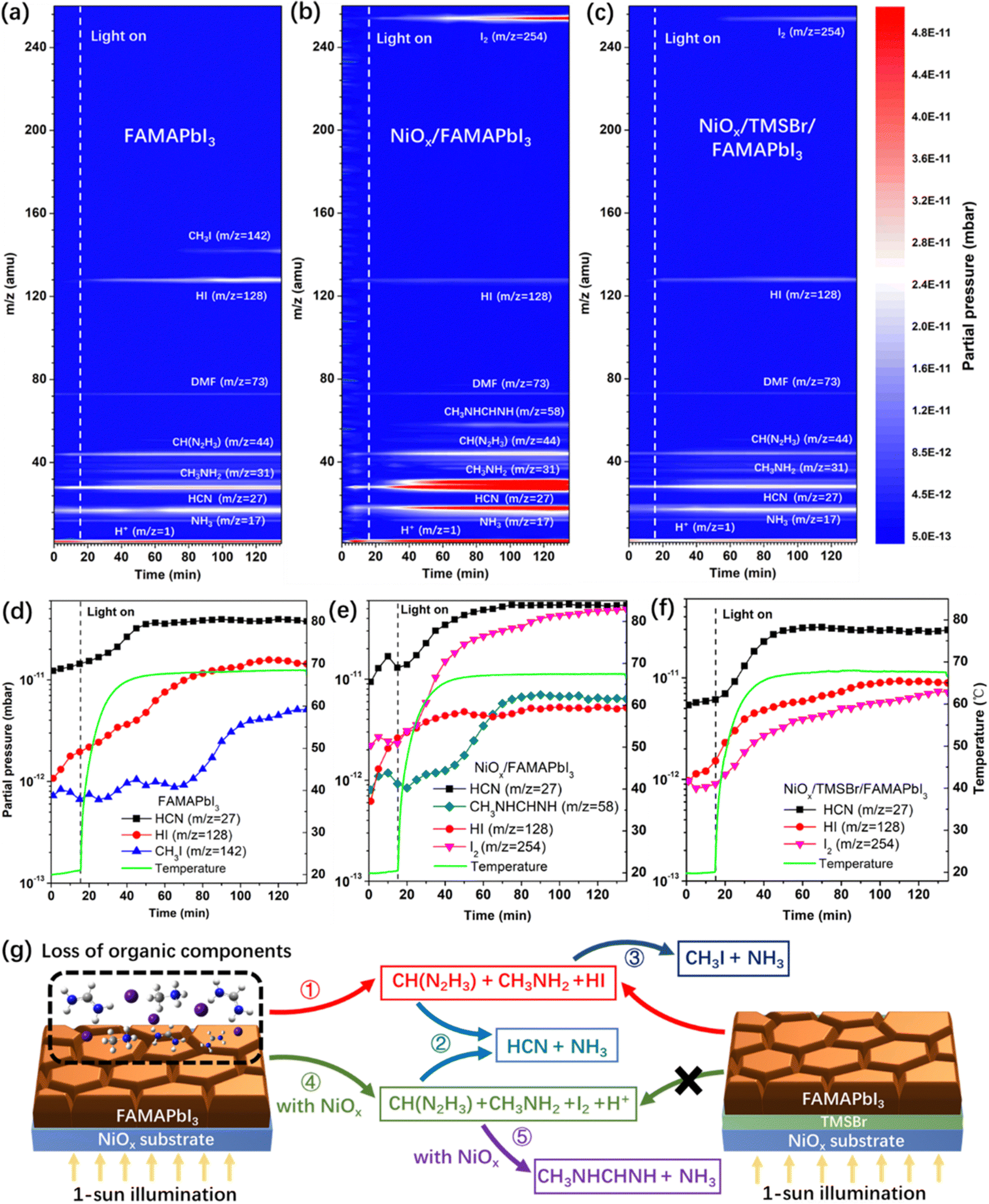 | ||
| Fig. 2 Light-induced degradation dynamics of the NiOx-FAMAPbI3 heterojunction. (a–c) Time-resolved MS contour plots (m/z = 1–260 amu) of (a) pure FAMAPbI3, (b) NiOx/FAMAPbI3, and (c) NiOx/TMSBr/FAMAPbI3 films coated on the FTO substrate, the simulated 1-sun light was applied after 15 min of the MS measurements. (d–f) Partial pressure of the signature degradation products and the sample temperature versus the illumination time for the (d) pure FAMAPbI3, (e) NiOx/FAMAPbI3, and (f) NiOx/TMSBr/FAMAPbI3. (g) Possible degradation mechanism of the FAMAPbI3 perovskite with NiOx contact under 1-sun illumination conditions. | ||
To verify the assignments of gas products in Fig. 2a–c, we also measured the time-resolved MS plots of NiOx/MAI, NiOx/FAI, and NiOx/(MAI + FAI) (with a similar FA/MA ratio to the perovskite) films under operational conditions (Fig. S7a–c, ESI†). For the NiOx/MAI sample, the released products of H+, NH3, CH3NH2, HI, CH3I, and I2 were detected, and the released products were H+, NH3, HCN, CH(N2H3), HI, and I2 for the NiOx/FAI sample. Moreover, the product of N-methyl formamidine was only found in the case of the NiOx/(FAI + MAI) sample, which further confirms the condensation reaction of MA and FA occurring at the NiOx/perovskite interface.
In contrast, we found that the partial pressure of I2 in the NiOx/TMSBr/FAMAPbI3 film was one order of magnitude lower than that in the NiOx/FAMAPbI3 film (Fig. 2f), along with the reduced pressure of MA, FA, and free protons. This result illustrates that the TMSBr buffer layer can efficiently suppress reaction 4 triggered by the NiOx contact, and thus suppress other side reactions (2, 3, and 5) at elevated temperature, as demonstrated in Fig. 2g. To identify the unique role of aprotic TMS+ in suppressing reaction 4, we further measured the time-resolved MS plots of the NiOx/FABr and NiOx/TMSBr samples (Fig. S8a and b, ESI†). The NiOx/FABr showed the degradation products of H+, NH3, HCN, CH(N2H3), and HBr (m/z = 81), while no degradation product was detected in the NiOx/TMSBr sample under continuous illumination. Besides, the cross-section SEM images were used to investigate the impact of released gas products on the morphology of the NiOx/perovskite interface (Fig. S9, ESI†). Some pinholes could be found at the NiOx/FAMAPbI3 interface after 2-hour illumination (MS test), which may retard the charge transfer process in solar cells and could be eliminated by incorporating the TMSBr buffer layer. For a comprehensive comparison, we further studied the degradation process of the tetramethylammonium bromide (TMABr) salt coated on the NiOx substrate under continuous 1-sun illumination. TMABr exhibited an aprotic nature and a molecular structure similar to that of the TMSBr, but the central atom is replaced by nitrogen. As shown in Fig. S8c (ESI†), we found two signals with the m/z ratios of 59 amu and 95 amu in the NiOx/TMABr film after 70 min illumination, associated with the gas products of N(CH3)3 and CH3Br, respectively. This result demonstrates that trimethylsulfonium is better than tetramethylammonium for mitigating the light-induced degradation at the NiOx/perovskite interface due to the higher dissociation energy barrier of the former one.47,48
XPS measurements were also conducted to further investigate the reaction between organic halide salts and NiOx under operational conditions. Fig. 3a and b show the evolution of the Ni 2p core level of the NiOx film coated with FAI and TMSBr under 1-sun illumination, respectively. It can be found that about 11.8 at% of Ni3+ (854.9 eV) was reduced to Ni2+ (853.5 eV) after 2-hour illumination for the NiOx/FAI sample while this change was negligible for NiOx/TMSBr. Besides, the proton-type NiOOH components (856.5 eV) increased from 10.4 at% to 14.3 at% for NiOx/FAI and were kept unchanged for NiOx/TMSBr, further confirming that proton-transfer and redox reactions could be eliminated by the TMSBr buffer layer. Moreover, we tracked the evolution of the N 1s core level to investigate the deprotonation process of FA+ on the NiOx surface (Fig. 3c). It can be seen that about 37 at% of the FA+ cations (400.6 eV) degraded to the neutral FA molecules (399.7 eV) after 2 hours of illumination. In contrast, the peak position and the intensity of the S 2p core level of the TMS+ cations showed a negligible change under the same aging conditions (Fig. 3d), which means that TMS+ could significantly retard the proton-transfer process at the NiOx/perovskite interface.
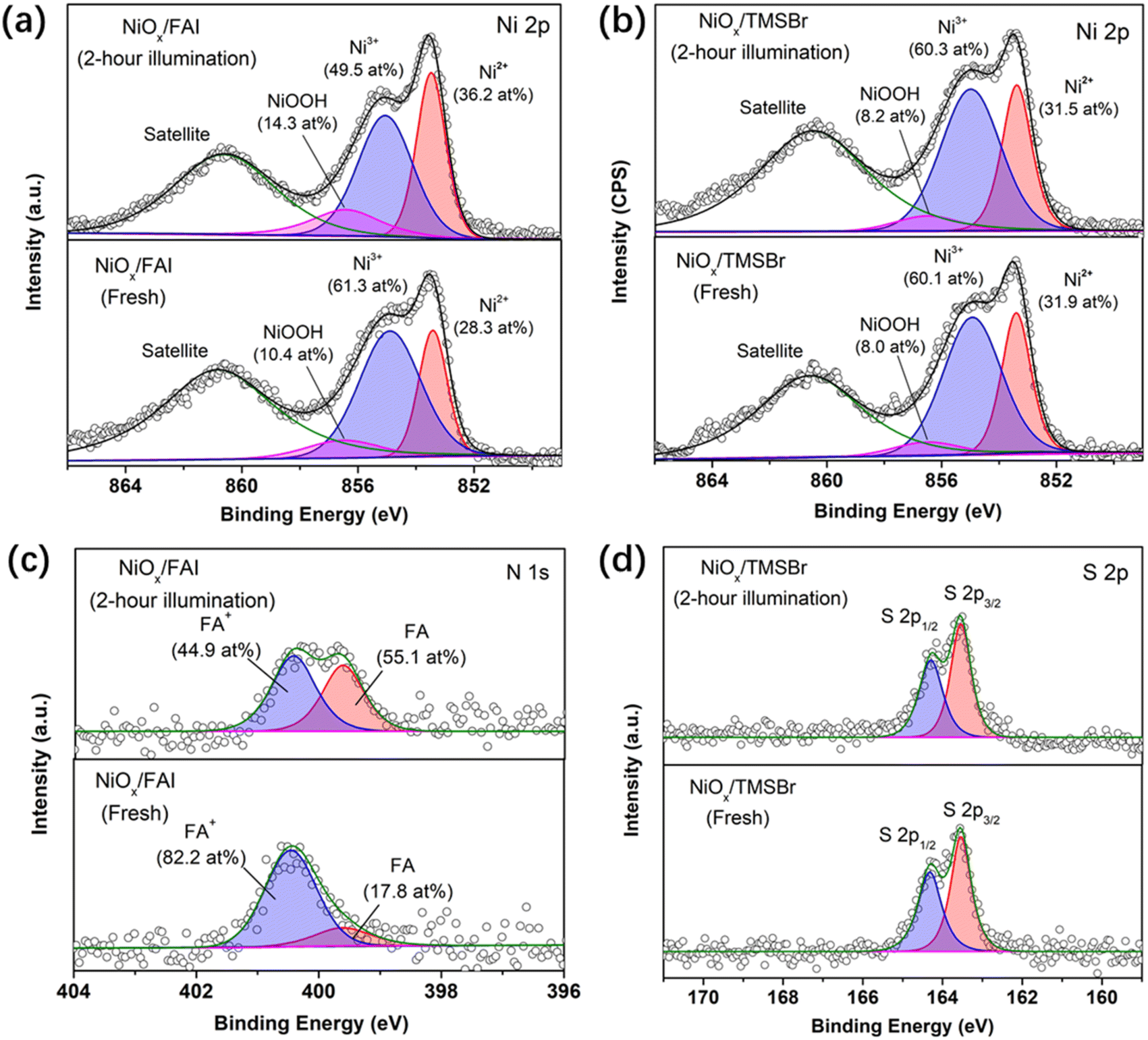 | ||
| Fig. 3 Reaction between NiOx and organic salts identified by the XPS analysis. (a and b) XPS Ni 2p spectra of (a) NiOx/FAI and (b) NiOx/TMSBr films before and after 1-sun illumination for 2 hours, the component at 860.6 eV is assigned to the shake-up satellite peak. (c) XPS N 1s spectra of the NiOx/FAI film before and after 1-sun illumination for 2 hours. (d) XPS S 2p spectra of the NiOx/TMSBr film before and after 1-sun illumination for 2 hours. | ||
Afterwards, we further studied the impact of TMS+ cations on the defect density of the NiOx–perovskite heterojunction. We calculated the trap density in the NiOx–perovskite heterojunction by measuring the dark current profiles of the hole-only device based on the space charge limit current (SCLC) method. Fig. 4a shows the dark current plots of the hole-only devices with a structure of FTO/NiOx/perovskite (without or with TMSBr)/poly(bis(4-phenyl)(2,4,6-trimethylphenyl)amine) (PTAA)/Ag, including an Ohmic regime, a trap-filled limited regime (TFL) and a trap-free space charge limited current (SCLC) regime (Child).49 The trap density can be deduced from the onset voltage of the TFL regime (VTFL), the trap densities for holes were calculated to be 2.72 × 10¹⁶ and 2.02 × 1016 cm−3 for the NiOx/FAMAPbI3 and NiOx/TMSBr/FAMAPbI3 samples, respectively, according to eqn (S1) in the ESI.† Also, we measured the SCLC plots of the electron-only device (FTO/C60/perovskite (without or with TMSBr)/C60/Ag) to track the change of trap densities for electrons. As shown in Fig. S10 (ESI†), the electron-only devices also showed a decrease in trap densities (from 2.48 × 10¹⁶ to 1.98 × 1016 cm−3) after incorporating TMSBr, indicating that passivation by TMSBr can realize a balance between electron and hole transport.
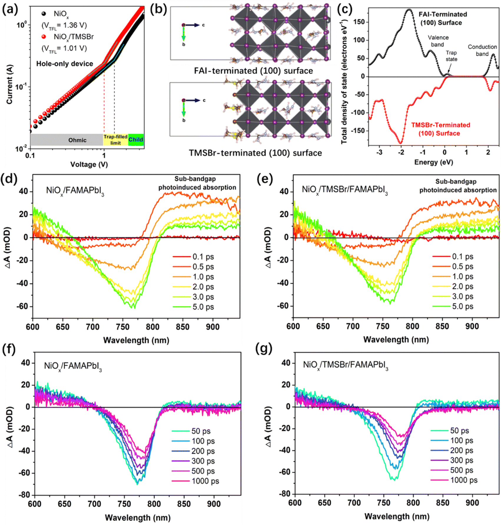 | ||
| Fig. 4 (a) Dark current plots of the hole-only devices with or without TMSBr treatment, three regions can be identified according to different values of the slope n: n = 1 is the Ohmic region, n = 2 is the SCLC region (Child), and n > 2 is the trap-filled limited region. (b) The FAI-terminated and TMSBr-terminated FAPbI3 (100) slabs after relaxation to the minimum energy, the white, brown, blue, yellow, gray, and purple spheres represent H, C, N, S, Pb, and I atoms, respectively. (c) Total density of state distribution plots of the FAI-terminated and TMSBr-terminated FAPbI3 models. (d–g) Delay time-dependent TA spectra (time scale: 0.1–5.0 ps and 50–1000 ps) for the (d and f) NiOx/FAMAPbI3 and (e and g) NiOx/TMSBr/FAMAPbI3 films coated on the glass substrate. | ||
Besides, DFT calculations were conducted to reveal the effect of TMS+ incorporation on the density of state (DOS) distribution of the perovskite lattice. Fig. 4b depicts the geometry-optimized FAI-terminated and TMS-terminated perovskite (100) slabs (a pure FAPbI3 model is used here to simplify the calculation process) and Fig. 4c shows the total DOS distribution plots near the valence and conduction band edges for the (100) slabs. It can be seen that the terminated TMS+ cation with a larger steric hindrance effect than FA+ could reduce the lattice distortion of [PbI6]4− frameworks at the surface (interface), a similar effect induced by the cations with a large steric hindrance (such as the tertiary and quaternary alkyl ammoniums) has also been reported by previous studies.50,51 We found that the TMSBr-terminated (100) slab shows a much lower DOS at the valence band edge compared to the FAI-terminated (100) slab associated with the reduction of the trap density. Besides, (111) and (210) FAPbI3 slabs (Fig. S11, ESI†) were also built to elucidate the impact of the TMSBr terminated layer on the DOS distribution of the perovskite lattice, we found similar trends of reduced DOS near the valence band edge by incorporating the TMSBr terminal layer (Fig. S12, ESI†).
The carrier transport and extraction processes at the heterojunction interface are critical factors to determine the solar cell performance; therefore, we further investigated the carrier dynamics at the NiOx–perovskite heterojunction by femtosecond transient absorption spectroscopy (TAS). As shown in Fig. 4d and e, a unique ground-state bleaching (GSB) peak of FAMAPbI3 perovskite was formed at around 759 nm along with the rapid decay of sub-bandgap photoinduced absorption at the delay time of 0.1–5.0 ps, related to the hot carrier relaxation process.52 A weaker sub-bandgap absorption in the NiOx/TMSBr/FAMAPbI3 film is associated with a lower trap density near the valence or conduction band edge. Besides, we can see a quenching of the GSB peak at the delay time of 50–1000 ps, the quenching rate of the GSB peak signal reflects the carrier transport efficiency from the perovskite to the NiOx contact.53 At the same delay time, the GSB peak intensity of the NiOx/TMSBr/FAMAPbI3 film is much weaker than the original value as well as that of the NiOx/FAMAPbI3 counterpart, indicating a better hole extraction efficiency at the TMSBr-incorporated NiOx/perovskite interface with a lower trap density at the valence band edge. Furthermore, we calculated the decay lifetime of GSB peaks to be 272 ps for the NiOx/FAMAPbI3 sample versus 178 ps for the NiOx/TMSBr/FAMAPbI3 sample, by analyzing the decay kinetics plots (Fig. S13, ESI†). In addition, we found a more obvious red shift of the GSB peak in the NiOx/TMSBr/FAMAPbI3 film, which demonstrates a carrier injection process from the TMSBr-rich phase (with a larger bandgap) to the pure FAMAPbI3 phase.
To study the impact of TMSBr incorporation on the photovoltaic performance of PSCs, we fabricated the inverted planar device with a structure of the FTO/NiOx/TMSBr/perovskite/donor–π–acceptor (D–π–A) passivator/PCBM/BCP/Ag (Fig. 5a). Here, the D–π–A molecule (N,N-dibutylaminophenyl as the electron donor, thiophene as the π-spacer, and cyanoacetic acid as the electron acceptor) with a dipolar electron density distribution was used to passivate the under-coordinated Pb2+ defects on the perovskite top surface, and served as a diffusion barrier to suppress the light-induced iodide migration into the Ag electrode that is another important factor to cause PSC degradation (the schematic illustration is shown in Fig. S14, ESI†), which has been comprehensively studied in our previous works.54,55 The J–V curves of the FAMAPbI3 PSCs (without and with TMSBr) are plotted in Fig. 5b, and the photovoltaic parameters of the champion devices are summarized in Table 1. The control devices give the best PCE of 19.46%, with a VOC of 1.14 V, a short-circuit current density (JSC) of 22.32 mA cm−2, and a fill factor (FF) of 76.48%. In contrast, the TMSBr-treated devices exhibit an enormous improvement in VOC and FF and present the best PCE up to 22.06%, showing a VOC of 1.18 V, a JSC of 22.96 mA cm−2, and a FF of 81.33%. The inset in Fig. 5b shows the cross-sectional SEM images of the TMSBr-treated PSCs, which contain a perovskite absorber with a thickness of 500–550 nm and a 50 nm electron transport layer. The J–V curves and photovoltaic parameters of the champion PSCs with 5 nm and 15 nm TMSBr are also shown in Fig. S15a and b (ESI†), respectively. It can be found that a relatively thicker TMSBr significantly increased the series resistance of the PSCs, resulting in a much lower FF (73.56%) than that of the control device (Table S1, ESI†). In addition, the statistical distribution plots of VOC (Fig. S15c, ESI†) and PCE (Fig. S15d, ESI†) of the devices demonstrate high reproducibility of the evaporated TMSBr buffer layer for producing efficient NiOx-based PSCs.
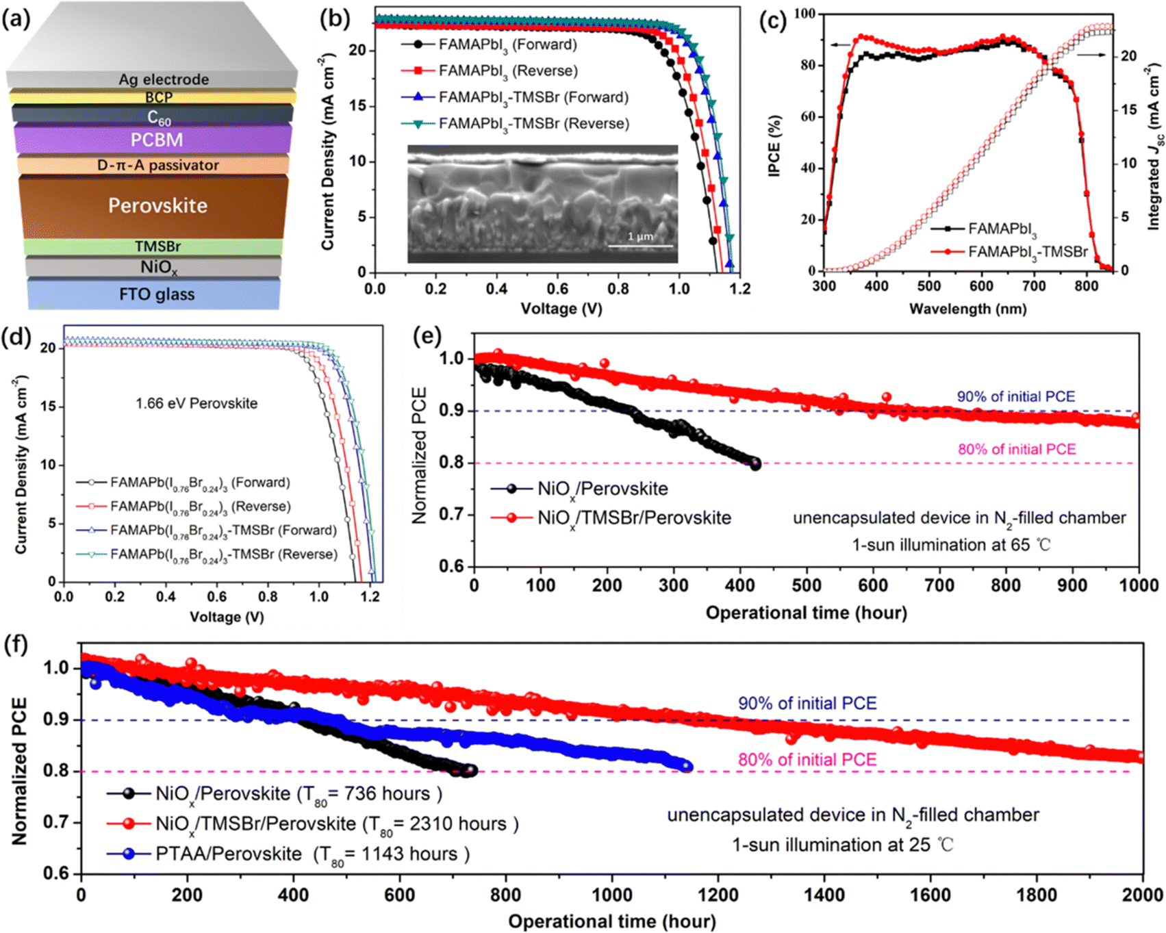 | ||
| Fig. 5 Device performance and stability. (a) Device structure of the inverted PSCs with the TMSBr buffer layer. (b) J–V curves of the inverted PSCs based on the 1.53 eV FAMAPbI3 absorber without and with TMSBr treatment, the inset shows the cross-sectional SEM image of the TMSBr-treated device. (c) IPCE spectra of the inverted PSCs based on the FAMAPbI3 absorber without and with TMSBr treatment. (d) J–V curves of the inverted PSCs based on a 1.66 eV FAMAPb(I0.76Br0.24)3 absorber without and with TMSBr treatment. (e) Operational stability of the PSCs measured under 65 °C at a fixed bias near the maximum power point. (f) Operational stability of the PSCs measured under room temperature (25 °C), these operational stability tests of PSCs represent the performance of the champion devices. | ||
| Perovskite | Scan direction | J SC (mA cm−2) | V OC (V) | FF (%) | PCE (%) |
|---|---|---|---|---|---|
| FAMAPbI3 (1.53 eV) | Forward | 22.37 | 1.12 | 75.02 | 18.79 |
| Reverse | 22.32 | 1.14 | 76.48 | 19.46 | |
| FAMAPbI3-TMSBr | Forward | 22.85 | 1.17 | 80.51 | 21.52 |
| Reverse | 22.96 | 1.18 | 81.33 | 22.06 | |
| FAMAPb(I0.76Br0.24)3 (1.66 eV) | Forward | 20.53 | 1.14 | 75.32 | 17.63 |
| Reverse | 20.45 | 1.16 | 77.21 | 18.32 | |
| FAMAPb(I0.76Br0.24)3-TMSBr | Forward | 20.73 | 1.21 | 78.05 | 19.58 |
| Reverse | 20.62 | 1.22 | 79.59 | 20.02 |
Fig. 5c shows the incident photon-to-current efficiency (IPCE) spectra of the corresponding device, we found that the IPCE increased significantly at the wavelength of 350–450 nm when a TMSBr buffer layer was incorporated. This increase in IPCE was associated with the improvement in carrier extraction efficiency at the illumination side (NiOx/perovskite interface), which further supports the results of the TAS measurements. The integrated JSC values of the PSCs without or with the TMSBr treatment were calculated to be 22.31 and 22.87 mA cm−2, respectively, close to those of the J–V measurements.
Moreover, we extended our strategy to the 1.66 eV wide-bandgap perovskite systems that are frequently used in the top cell of silicon-perovskite tandem solar cells.56,57 We fabricated the wide-bandgap perovskite absorber by doping excess Br− into the FAMAPbI3 system. By controlling the I/Br ratio at around 0.76/0.24 (identified by the XPS I 3d and Br 3d spectra in Fig. S16a, ESI†), the perovskite absorber with an absorption edge at 746 nm (1.66 eV) could be obtained (Fig. S16b, ESI†). Similar to the trend in the FAMAPbI3 system, the incorporation of TMSBr at the NiOx/FAMAPb(I0.76Br0.24)3 perovskite interface reduced the content of the PbI1−xBrx phase (Fig. S16c, ESI†). The SEM top-view images (Fig. S16d and e, ESI†) show that a compact polycrystalline morphology of the FAMAPb(I0.76Br0.24)3 perovskite films with a grain size of 500–1000 nm could be achieved using a sequential deposition method. We further fabricated the 1.66 eV inverted PSCs based on the same device structure to evaluate their photovoltaic performance. Fig. 5d shows the J–V curves of the FAMAPb(I0.76Br0.24)3-based PSCs, and the control devices exhibit the best PCE of 18.32%, with a VOC of 1.16 V, a JSC of 20.45 mA cm−2, and a FF of 77.21%. By contrast, the TMSBr-treated devices give a higher PCE of 20.02%, with a promising VOC up to 1.22 V, a JSC of 20.62 mA cm−2, and a FF of 79.59%. The above results further demonstrate that the TMSBr buffer layer should be a universal passivation strategy to improve the VOC and efficiency of inverted PSCs with a variety of perovskite compositions.
We evaluated the device operational stability under accelerated-ageing conditions according to the International Summit on Organic Photovoltaic Stability (ISOS) protocols using our home-designed test system (Fig. S17, ESI†).58 A bias close to the voltage at the maximum power point (MPP) was applied to track the power output of the corresponding inverted PSCs in the N2-filled chamber with ∼5% relative humidity, and the device temperature during the operation was monitored using a thermocouple. Fig. 5e shows the PCE decay plots of the unencapsulated NiOx/FAMAPbI3 PSCs without and with the TMSBr buffer layer measured under 1-sun illumination at 65 °C (ISOS-L-2I), the PCE of the control device decreased to 80% of its initial value after operation for about 430 hours, while the PCE of TMSBr-stabilized PSCs kept about 88% of the initial value after operation for 1000 hours. Fig. S18 (ESI†) depicts the cross-sectional SEM images of the aged devices after the 65 °C operation test, many pinholes can be found inside the perovskite layer near the NiOx/perovskite interface, which was induced by the I2 vapor and other volatile products that could corrode the perovskite layer,59 as confirmed by the MS results. In contrast, the TMSBr-stabilized device still kept a pinhole-free compact perovskite layer after the operational stability test, which emphasizes the importance of the TMSBr buffer layer in suppressing the multi-step degradation of the NiOx–perovskite heterojunction.
In addition, the PCE decay plots of the unencapsulated devices under 1-sun illumination at room temperature (ISOS-L-1I) were also measured (Fig. 5f), and the decay plots with the real efficiency value are provided in Fig. S19 (ESI†). The T80 value of the TMSBr-stabilized device was estimated to be 2310 hours according to the constant PCE decay rate of 0.009% per hour during the operational process (2000-hour measurement), which is much higher than that of the control device (736 hours) and is among the highest value compared to the state-of-the-art NiOx-based inverted PSCs (the reported operational lifetimes were summarized in Table S2, ESI†). To understand the reproducibility of our stability measurement, we further tracked the efficiency decay profiles of 6 individual cells in one batch under the same condition (1-sun illumination at 25 °C with dry N2 flow) and then extracted the average T80 operational lifetime. As shown in Fig. S20 (ESI†), the T80 lifetime of the NiOx/perovskite PSCs is estimated to be (7.1 ± 0.3) × 100 hours based on calculating the PCE decay rates of each device under 300-hour operation time. By contrast, the NiOx/TMSBr/perovskite PSCs show a much longer T80 lifetime of (22.8 ± 0.4) × 100 hours based on the same calculation method. We also found that the devices in the same group exhibited a similar PCE decay rate and a small deviation of the T80 value, which indicates the high reproducibility of our stability measurement and our solar cells.
As a comparison, the inverted PSCs based on a widely used PTAA hole transport layer without any chemical dopants were fabricated for the operational stability test. According to the PCE decay curves, the PTAA-based device using FAMAPbI3 absorber exhibits a T80 lifetime of 1143 hours, the PCE loss may be caused by the degradation of the conjugated triphenylamine frameworks of PTAA triggered by the high-energy UV light under continuous 1-sun illumination.24 Fig. S21a (ESI†) illustrated the device structure of the PTAA-based device that was similar to the NiOx-based counterpart, which enables the best PCE of about 19.6% (the device parameters were summarized in Table S3 (ESI†), and the IPCE spectrum in Fig. S21b (ESI†) was used for JSC calibration) and exhibited a similar perovskite thickness of 500–550 nm compared to NiOx-based counterpart (Fig. S21c, ESI†). Moreover, we found that the TMSBr buffer layer also improved the operational stability of the wide-bandgap PSCs significantly. As demonstrated in Fig. S22 (ESI†), the TMSBr-stabilized FAMAPb(I0.76Br0.24)3 device retained 97.5% of the initial efficiency after continuous operation at the MPP condition for 500 hours, while the control device retained about 88.9% of the initial efficiency.
Although the TMSBr stabilization strategy endows the NiOx-based PSCs with a significant stability improvement, the devices still undergo a certain efficiency loss during the operation process. To further enhance the operational stability, the following issues need to be addressed: (1) corrosion of the metal rear electrode by the released iodide species from the perovskite layer is a major factor that causes the efficiency loss under operational conditions, and the development of graphene-based electrode materials with both good conductivity and good chemical stability will be a promising way to overcome this problem, which has been an active research topic in recent years;60 (2) light-induced iodide migration into the fullerene-based electron transport layer could retard the electron extraction process and lead to the decay of PCE, thus constructing a compact ion diffusion barrier is also critical for further stability improvement;9 (3) developing the encapsulation materials that can not only block the outside moisture and oxygen but also retard the escape of volatile components under light and thermal stresses is a key strategy to realize a robust operational stability of PSCs under severe weather conditions.61
Conclusions
In summary, we clarified the unique degradation dynamics of a NiOx–perovskite heterojunction under the operational conditions of a device, and a strategy based on the buffer layer with aprotic nature, good photo-thermal stability, and matched lattice parameter with a perovskite absorber was successfully proposed to eliminate the multi-step reactions, enabling a record operational lifetime over 2000 hours for the NiOx-based PSCs. Also, we clarified that the TMSBr buffer layer is a promising passivation route to improve the device's open-circuit voltage, which produces a VOC of 1.18 V for 1.53 eV bandgap PSCs and a VOC of 1.22 V for 1.66 eV bandgap PSCs. Our work provides a novel understanding of the interface chemistry between perovskite and metal oxide layers under operational conditions and could be extended to other compositions or device structures in future studies. Also, our fabrication techniques including the spray pyrolysis and vacuum vapor-deposition methods enable the up-scaling deposition of the uniform NiOx–perovskite heterojunction in inverted PSCs toward efficient and long-term stable large-area solar modules. With respect to the wet deposition technique for large-area solar modules, most of the functional layers used in our inverted structured PSCs, including the hole-selective NiOx layer, perovskite layer, and the electron-selective fullerene layer, can be deposited through the blade coating, slot-die coating or printing technique. On the other hand, the TMSBr layer in this work is very thin (5–10 nm) and may not be straightforwardly printable toward the large-area and uniform film. Therefore, more efforts to study the wet deposition methods of aprotic sulfonium salts, such as the blade coating and slot-die coating, are urgently needed in the future.Author contributions
Y. B. Q. supervised this research project. T. W. and Y. B. Q. conceived the experiments, performed the data analysis, and wrote the manuscript. T. W., L. H., and Y. B. Q. participated in the discussion about the experimental details. T. W. and J. Z. conducted the solar cell fabrication. K. M. helped with the transient absorption spectroscopy measurements. R. Y., K. M., R. K., X. L., S. M., H. S. and C. D. helped with the sample preparation for characterization. T. W., L. K. O., C. Z. and R. Y. conducted the characterization.Conflicts of interest
The authors declare no competing interests.Acknowledgements
This work was supported by funding from the Energy Materials and Surface Sciences Unit of the Okinawa Institute of Science and Technology Graduate University, the OIST R & D Cluster Research Program, the OIST Proof of Concept (POC) Program, and JST A-STEP Grant Number JPMJTM20HS, Japan. We thank the OIST Micro/Nanofabrication Section and Imaging Section for the support. Prof. L. H. thanks the National Natural Science Foundation of China (12074245 and U21A20171) and the JSPS KAKENHI Grant (21H02040).References
- J. J. Yoo, G. Seo, M. R. Chua, T. G. Park, Y. Lu, F. Rotermund, Y. K. Kim, C. S. Moon, N. J. Jeon, J. P. Correa-Baena, V. Bulović, S. S. Shin, M. G. Bawendi and J. Seo, Nature, 2021, 590, 587–593 CrossRef CAS.
- Z. Li, B. Li, X. Wu, S. A. Sheppard, S. Zhang, D. Gao, N. J. Long and Z. Zhu, Science, 2022, 376, 416–420 CrossRef CAS PubMed.
- H. Chen, S. Teale, B. Chen, Y. Hou, L. Grater, T. Zhu, K. Bertens, S. M. Park, H. R. Atapattu, Y. Gao, M. Wei, A. K. Johnston, Q. Zhou, K. Xu, D. Yu, C. Han, T. Cui, E. H. Jung, C. Zhou, W. Zhou, A. H. Proppe, S. Hoogland, F. Laquai, T. Filleter, K. R. Graham, Z. Ning and E. H. Sargent, Nat. Photonics, 2022, 16, 352–358 CrossRef CAS.
- T. Wu, Z. Qin, Y. Wang, Y. Wu, W. Chen, S. Zhang, M. Cai, S. Dai, J. Zhang, J. Liu, Z. Zhou, X. Liu, H. Segawa, H. Tan, Q. Tang, J. Fang, Y. Li, L. Ding, Z. Ning, Y. B. Qi, Y. Zhang and L. Han, Nano-Micro Lett., 2021, 13, 152 CrossRef CAS PubMed.
- Y. Wang, T. Wu, J. Barbaud, W. Kong, D. Cui, H. Chen, X. Yang and L. Han, Science, 2019, 365, 687–691 CrossRef CAS PubMed.
- S. Yang, S. Chen, E. Mosconi, Y. Fang, X. Xiao, C. Wang, Y. Zhou, Z. Yu, J. Zhao, Y. Gao, F. De Angelis and J. Huang, Science, 2019, 365, 473–478 CrossRef CAS PubMed.
- L. Xu, X. Chen, J. Jin, W. Liu, B. Dong, X. Bai, H. Song and P. Reiss, Nano Energy, 2019, 63, 103860 CrossRef CAS.
- T. Wu, X. Liu, X. Luo, H. Segawa, G. Tong, Y. Zhang, L. K. Ono, Y. B. Qi and L. Han, Nano-Micro Lett., 2022, 14, 99 CrossRef CAS.
- E. Bi, W. Tang, H. Chen, Y. Wang, J. Barbaud, T. Wu, W. Kong, P. Tu, H. Zhu, X. Zeng, J. He, S. I. Kan, X. Yang, M. Grätzel and L. Han, Joule, 2019, 3, 2748–2760 CrossRef CAS.
- W. Chen, B. Han, Q. Hu, M. Gu, Y. Zhu, W. Yang, Y. Zhou, D. Luo, F. Z. Liu, R. Cheng, R. Zhu, S. P. Feng, A. B. Djurišić, T. P. Russell and Z. He, Sci. Bull., 2021, 66, 991–1002 CrossRef CAS.
- F. Sadegh, S. Akin, M. Moghadam, R. Keshavarzi, V. Mirkhani, M. A. Ruiz-Preciado, E. Akman, H. Zhang, M. Amini, S. Tangestaninejad, I. Mohammadpoor-Baltork, M. Graetzel, A. Hagfeldt and W. Tress, Adv. Funct. Mater., 2021, 31, 2102237 CrossRef CAS.
- C. C. Boyd, R. C. Shallcross, T. Moot, R. Kerner, L. Bertoluzzi, A. Onno, S. Kavadiya, C. Chosy, E. J. Wolf, J. Werner, J. A. Raiford, C. de Paula, A. F. Palmstrom, Z. J. Yu, J. J. Berry, S. F. Bent, Z. C. Holman, J. M. Luther, E. L. Ratcliff, N. R. Armstrong and M. D. McGehee, Joule, 2020, 4, 1759–1775 CrossRef CAS.
- G. Li, Y. Jiang, S. Deng, A. Tam, P. Xu, M. Wong and H. S. Kwok, Adv. Sci., 2017, 4, 1700463 CrossRef PubMed.
- S. Seo, S. Jeong, C. Bae, N. G. Park and H. Shin, Adv. Mater., 2018, 30, 1801010 CrossRef PubMed.
- S. Wang, Y. Li, J. Yang, T. Wang, B. Yang, Q. Cao, X. Pu, L. Etgar, J. Han, J. Zhao, X. Li and A. Hagfeldt, Angew. Chem., Int. Ed., 2022, 61, 202116534 Search PubMed.
- F. Ma, Y. Zhao, J. Li, X. Zhang, H. Gu and J. You, J. Energy Chem., 2021, 52, 393–411 CrossRef.
- Y. Zheng, B. Ge, L. R. Zheng, Y. Hou, S. Yang and H. G. Yang, J. Mater. Chem. A, 2021, 9, 21792–21798 RSC.
- K. C. Hsiao, B. T. Lee, M. H. Jao, T. H. Lin, C. H. Hou, J. J. Shyue, M. C. Wu and W. F. Su, Chem. Eng. J., 2021, 409, 128100 CrossRef CAS.
- Y. Guo, J. Ma, H. Wang, F. Ye, L. Xiong, H. Lei and Z. Tan, Adv. Mater. Interfaces, 2021, 8, 2100920 CrossRef CAS.
- J. Sun, C. Shou, J. Sun, X. Wang, Z. Yang, Y. Chen, J. Wu, W. Yang, H. Long, Z. Ying, X. Yang, J. Sheng, B. Yan and J. Ye, Sol. RRL, 2021, 5, 2100663 CrossRef CAS.
- J. Zhang, J. Long, Z. Huang, J. Yang, X. Li, R. Dai, W. Sheng, L. Tan and Y. Chen, Chem. Eng. J., 2021, 426, 131357 CrossRef CAS.
- T. Guo, Z. Fang, Z. Zhang, Z. Deng, R. Zhao, J. Zhang, M. Shang, X. Liu, Z. Hu, Y. Zhu and L. Han, J. Energy Chem., 2022, 69, 211–220 CrossRef.
- Z. Li, B. H. Jo, S. J. Hwang, T. H. Kim, S. Somasundaram, E. Kamaraj, J. Bang, T. K. Ahn, S. Park and H. J. Park, Adv. Sci., 2019, 6, 1802163 CrossRef PubMed.
- X. Liu, Y. Cheng, C. Liu, T. Zhang, N. Zhang, S. Zhang, J. Chen, Q. Xu, J. Ouyang and H. Gong, Energy Environ. Sci., 2019, 12, 1622–1633 RSC.
- B. Zhang, J. Su, X. Guo, L. Zhou, Z. Lin, L. Feng, J. Zhang, J. Chang and Y. Hao, Adv. Sci., 2020, 7, 1903044 CrossRef CAS.
- W. Chen, Y. Zhou, G. Chen, Y. Wu, B. Tu, F. Z. Liu, L. Huang, A. M. C. Ng, A. B. Djurišić and Z. He, Adv. Energy Mater., 2019, 9, 1803872 CrossRef.
- J. P. Correa-Baena, Y. Luo, T. M. Brenner, J. Snaider, S. Sun, X. Li, M. A. Jensen, N. T. P. Hartono, L. Nienhaus, S. Wieghold, J. R. Poindexter, S. Wang, Y. S. Meng, T. Wang, B. Lai, M. V. Holt, Z. Cai, M. G. Bawendi, L. Huang, T. Buonassisi and D. P. Fenning, Science, 2019, 363, 627–631 CrossRef CAS PubMed.
- A. Kaltzoglou, C. C. Stoumpos, A. G. Kontos, G. K. Manolis, K. Papadopoulos, K. G. Papadokostaki, V. Psycharis, C. C. Tang, Y. K. Jung, A. Walsh, M. G. Kanatzidis and P. Falaras, Inorg. Chem., 2017, 56, 6302–6309 CrossRef CAS.
- M. M. Rahman, A. Ahmed, C. Y. Ge, R. Singh, K. Yoo, S. Sandhu, S. Kim and J. J. Lee, Sustainable Energy Fuels, 2021, 5, 4327–4335 RSC.
- M. M. Rahman, C. Y. Ge, K. Yoo and J. J. Lee, Mater. Today Energy, 2021, 21, 100803 CrossRef CAS.
- B. Kim, M. Kim, J. H. Lee and S. I. Seok, Adv. Sci., 2020, 7, 1901840 CrossRef CAS PubMed.
- W. Chen, Y. Wu, Y. Yue, J. Liu, W. Zhang, X. Yang, H. Chen, E. Bi, I. Ashraful, M. Gratzel and L. Han, Science, 2015, 350, 944–948 CrossRef CAS PubMed.
- M. Kim, G. H. Kim, T. K. Lee, I. W. Choi, H. W. Choi, Y. Jo, Y. J. Yoon, J. W. Kim, J. Lee, D. Huh, H. Lee, S. K. Kwak, J. Y. Kim and D. S. Kim, Joule, 2019, 3, 2179–2192 CrossRef CAS.
- Q. Jiang, L. Zhang, H. Wang, X. Yang, J. Meng, H. Liu, Z. Yin, J. Wu, X. Zhang and J. You, Nat. Energy, 2016, 2, 16177 CrossRef.
- P. H. Svensson and L. Kloo, Acta Crystallogr. C, 1996, 52, 2580–2581 CrossRef.
- Q. Jiang, Z. Chu, P. Wang, X. Yang, H. Liu, Y. Wang, Z. Yin, J. Wu, X. Zhang and J. You, Adv. Mater., 2017, 29, 1703852 CrossRef.
- W. T. M. Van Gompel, R. Herckens, G. Reekmans, B. Ruttens, J. D’Haen, P. Adriaensens, L. Lutsen and D. Vanderzande, J. Phys. Chem. C, 2018, 122, 4117–4124 CrossRef CAS.
- P. Haiss and K. P. Zeller, Org. Biomol. Chem., 2011, 9, 7748–7754 RSC.
- K. T. Cho, G. Grancini, Y. Lee, E. Oveisi, J. Ryu, O. Almora, M. Tschumi, P. A. Schouwink, G. Seo, S. Heo, J. Park, J. Jang, S. Paek, G. Garcia-Belmonte and M. K. Nazeeruddin, Energy Environ. Sci., 2018, 11, 952–959 RSC.
- T. Wu, D. Cui, X. Liu, X. Meng, Y. Wang, T. Noda, H. Segawa, X. Yang, Y. Zhang and L. Han, Sol. RRL, 2020, 4, 2000240 CrossRef CAS.
- E. J. Juarez-Perez, Z. Hawash, S. R. Raga, L. K. Ono and Y. B. Qi, Energy Environ. Sci., 2016, 9, 3406–3410 RSC.
- A. Mei, Y. Sheng, Y. Ming, Y. Hu, Y. Rong, W. Zhang, S. Luo, G. Na, C. Tian, X. Hou, Y. Xiong, Z. Zhang, S. Liu, S. Uchida, T. W. Kim, Y. Yuan, L. Zhang, Y. Zhou and H. Han, Joule, 2020, 4, 2646–2660 CrossRef CAS.
- E. J. Juarez-Perez, L. K. Ono and Y. B. Qi, J. Mater. Chem. A, 2019, 7, 16912–16919 RSC.
- L. Shi, M. P. Bucknall, T. L. Young, M. Zhang, L. Hu, J. Bing, D. S. Lee, J. Kim, T. Wu, N. Takamure, D. R. McKenzie, S. Huang, M. A. Green and A. W. Y. Ho-Baillie, Science, 2020, 368, eaba2412 CrossRef CAS PubMed.
- X. Wang, Y. Fan, L. Wang, C. Chen, Z. Li, R. Liu, H. Meng, Z. Shao, X. Du, H. Zhang, G. Cui and S. Pang, Chem, 2020, 6, 1369–1378 CAS.
- R. Liu, Z. Li, C. Chen, Y. Rao, X. Sun, L. Wang, X. Wang, Z. Zhou, T. Jiu, X. Guo, S. Frank Liu and S. Pang, ACS Appl. Mater. Interfaces, 2020, 12, 35043–35048 CrossRef CAS PubMed.
- Y. Nakazono, N. Ohmori, E. Araki, M. Hata, T. Hoshino and M. Tsuda, J. Photopolym. Sci. Tec., 1996, 9, 693–696 CrossRef CAS.
- M. Sawicka, P. Storoniak, P. Skurski, J. Błażejowski and J. Rak, Chem. Phys., 2006, 324, 425–437 CrossRef CAS.
- K. Wang, Z. Jin, L. Liang, H. Bian, H. Wang, J. Feng, Q. Wang and S. Liu, Nano Energy, 2019, 58, 175–182 CrossRef CAS.
- H. Chen, Q. Wei, M. I. Saidaminov, F. Wang, A. Johnston, Y. Hou, Z. Peng, K. Xu, W. Zhou, Z. Liu, L. Qiao, X. Wang, S. Xu, J. Li, R. Long, Y. Ke, E. H. Sargent and Z. Ning, Adv. Mater., 2019, 31, 1903559 CrossRef CAS PubMed.
- S. Yang, Y. Wang, P. Liu, Y. B. Cheng, H. J. Zhao and H. G. Yang, Nat. Energy, 2016, 1, 15016 CrossRef CAS.
- S. Narra, E. Jokar, O. Pearce, C. Y. Lin, A. Fathi and E. W. G. Diau, J. Phys. Chem. Lett., 2020, 11, 5699–5704 CrossRef CAS PubMed.
- Y. N. Lu, J. X. Zhong, Y. Yu, X. Chen, C. Y. Yao, C. Zhang, M. Yang, W. Feng, Y. Jiang, Y. Tan, L. Gong, X. Wei, Y. Zhou, L. Wang and W. Q. Wu, Energy Environ. Sci., 2021, 14, 4048–4058 RSC.
- T. Wu, Y. Wang, X. Li, Y. Wu, X. Meng, D. Cui, X. Yang and L. Han, Adv. Energy Mater., 2019, 9, 1803766 CrossRef.
- T. Wu, X. Li, Y. B. Qi, Y. Zhang and L. Han, ChemSusChem, 2021, 14, 4354–4376 CrossRef CAS PubMed.
- Y. H. Lin, N. Sakai, P. Da, J. Wu, H. C. Sansom, A. J. Ramadan, S. Mahesh, J. Liu, R. D. J. Oliver, J. Lim, L. Aspitarte, K. Sharma, P. K. Madhu, A. B. Morales-Vilches, P. K. Nayak, S. Bai, F. Gao, C. R. M. Grovenor, M. B. Johnston, J. G. Labram, J. R. Durrant, J. M. Ball, B. Wenger, B. Stannowski and H. J. Snaith, Science, 2020, 369, 96–102 CrossRef CAS PubMed.
- X. Luo, T. Wu, Y. Wang, X. Lin, H. Su, Q. Han and L. Han, Sci. China: Chem., 2021, 64, 218–227 CrossRef CAS.
- M. V. Khenkin, E. A. Katz, A. Abate, G. Bardizza, J. J. Berry, C. Brabec, F. Brunetti, V. Bulović, Q. Burlingame, A. Di Carlo, R. Cheacharoen, Y. B. Cheng, A. Colsmann, S. Cros, K. Domanski, M. Dusza, C. J. Fell, S. R. Forrest, Y. Galagan, D. Di Girolamo, M. Grätzel, A. Hagfeldt, E. von Hauff, H. Hoppe, J. Kettle, H. Köbler, M. S. Leite, S. Liu, Y. L. Loo, J. M. Luther, C. Q. Ma, M. Madsen, M. Manceau, M. Matheron, M. McGehee, R. Meitzner, M. K. Nazeeruddin, A. F. Nogueira, Ç. Odabaşı, A. Osherov, N. G. Park, M. O. Reese, F. De Rossi, M. Saliba, U. S. Schubert, H. J. Snaith, S. D. Stranks, W. Tress, P. A. Troshin, V. Turkovic, S. Veenstra, I. Visoly-Fisher, A. Walsh, T. Watson, H. Xie, R. Yıldırım, S. M. Zakeeruddin, K. Zhu and M. Lira-Cantu, Nat. Energy, 2020, 5, 35–49 CrossRef.
- S. Wang, Y. Jiang, E. J. Juarez-Perez, L. K. Ono and Y. B. Qi, Nat. Energy, 2017, 2, 16195 CrossRef CAS.
- H. Su, T. Wu, D. Cui, X. Lin, X. Luo, Y. Wang and L. Han, Small Methods, 2020, 4, 2000507 CrossRef CAS.
- Y. Jiang, L. Qiu, E. J. Juarez-Perez, L. K. Ono, Z. Hu, Z. Liu, Z. Wu, L. Meng, Q. Wang and Y. B. Qi, Nat. Energy, 2019, 4, 585–593 CrossRef CAS.
Footnote |
| † Electronic supplementary information (ESI) available. See DOI: https://doi.org/10.1039/d2ee01801b |
| This journal is © The Royal Society of Chemistry 2022 |