
 Open Access Article
 This Open Access Article is licensed under a
 Creative Commons Attribution 3.0 Unported Licence
Performance limitations imposed by the TCO heterojunction in high efficiency perovskite solar cells†
Daniel
Walter‡
 *a,
Jun
Peng‡
abc,
Klaus
Weber
a,
Kylie R.
Catchpole
a and
Thomas P.
White
*a
*a,
Jun
Peng‡
abc,
Klaus
Weber
a,
Kylie R.
Catchpole
a and
Thomas P.
White
*a
aSchool of Engineering, The Australian National University, Canberra, Australian Capital Territory, Australia. E-mail: daniel.walter@anu.edu.au; thomas.white@anu.edu.au
bInstitute of Functional Nano & Soft Materials (FUNSOM), Joint International Research Laboratory of Carbon-Based Functional Materials and Devices, Soochow University, Suzhou, Jiangsu 215123, P. R. China
cJiangsu Key Laboratory of Advanced Negative Carbon Technologies, Soochow University, Suzhou, Jiangsu 215123, P. R. China
First published on 28th October 2022
Abstract
The power conversion efficiency of perovskite solar cells (PSCs) has risen rapidly, but continuing this trend requires a clear view of all possible sources of power loss. Over the past decade in which we have witnessed these remarkable improvements, the transparent conductive oxide (TCO) has been widely treated as an extrinsic element. While it is recognised that the TCO contributes power loss due to finite lateral resistance and optical losses, comparatively little attention has been paid to the influence of the TCO on the electrostatics in other cell layers. However, a recent fill factor (FF) record on a centimetre-scale PSC has refocused attention on how the TCO can play a significant role in the optoelectronic properties across the entire TCO-transport layer-perovskite interface. Primarily, this is the consequence of the Schottky-type heterojunction formed between the TL and TCO layers, which establishes a space-charge region within the TL. Due to the extreme thinness of many TL layers, the space charge region can extend the full width of the TL and even into the perovskite layer itself. In effect, the bulk properties of the TL come to be dominated by the equilibrium conditions of this junction, with the consequence that the TL can be markedly less conductive once in situ within a PSC. This in situ resistance can significantly reduce FF, but without knowledge of this mechanism, the source of resistance and FF loss would be non-obvious. In this contribution, we employ ionic–electronic device models to quantify the TCO-induced in situ conductance of the transport layer and demonstrate its characteristic appearance in the JV curves of high-performance PSCs. We posit that widely used titanium dioxide (TiO2) can be particularly susceptible to a low in situ conductance, which explains the years-long plateau of FFs in TiO2-based PSCs in the low 80%-range. By comparison to inverted PSCs, we illustrate how the TCO influence can explain comparative underperformance of FF relative to open-circuit voltage and photocurrent in state-of-the-art n–i–p PSCs. We hope that by refocusing attention on this factor of PSC design, this work can provide a facile path to plausibly lifting single junction PSCs beyond 26% efficiency.
Broader contextSingle junction, small area perovskite solar cell (PSC) efficiency now sits at a remarkable 25.7%, close to the record for crystalline silicon at 26.6%, and closing in on the theoretical limit of circa 30–31%. Further efficiency gains will be increasingly difficult, motivating a close, careful look at possible sources of power loss in state-of-the-art PSCs. A notable limitation in n–i–p PSCs is fill factor (FF), which has historically lagged improvements in open-circuit voltage and photocurrent. In this work, we draw upon our group's recent FF record >86% to argue that the electrostatics of the transparent conductive oxide (TCO)-transport layer-perovskite interface plays a critical role in determining resistive power losses in the TL, and hence FF. These losses can be much larger than predictions based on TL conductivity alone. Thus, we provide explanations for the generally disappointing fill factors achieved with TiO2-based PSCs and the high FFs achieved in inverted (p–i–n) PSCs. In doing so, we identify transport layer properties that mitigate this performance limit. Ultimately, we argue that future theoretical and experimental work in PSCs must account for the interactions between all layers of the PSC electrodes to push efficiencies to 26% and beyond. |
Introduction
The transparent conductive oxide (TCO) constitutes the sunward-facing electrode of a perovskite solar cell (PSC) in single-junction or tandem configurations and conducts electric charge between the active cell layers and an external circuit. To date, the TCO has been widely treated as a passive cell component that has no direct bearing on charge conductivity within the PSC itself. In theoretical treatments (i.e. numerical device simulations) the influence of the TCO is rarely considered. However, a recent result from our group presents strong evidence that the TCO layer, through the heterojunction it forms with the sunward-facing transport layer (TL) can be influential on both the conductivity of the TL and to a lesser extent on non-radiative recombination within the perovskite layer itself. This result was a certified fill factor (FF) of more than 86% (PCE = 23.3%) on a 1 cm2 n–i–p PSC.1 This FF was an average improvement of ∼6% absolute over a control structure, characterised by a reduction in the series resistance component of the JV curve and a small improvement in open circuit voltage (Fig. 1). Remarkably, the control and high-efficiency devices were distinguished by a single structural change: substitution of a solution processed, lowly doped TiO2 film (ND ≈ 5 × 1014 cm−3) for a heavily doped titanium oxy-nitride (TiOxNy) film (ND ≈ 3 × 1017 cm−3) as the electron transport layer (ETL). Characterisation of these ETL materials showed that the only conclusive difference was the circa three order-of-magnitude increase in n-type ionized dopant density, with no significant change in other relevant properties such as electron affinity, bandgap, electron mobility and the perovskite crystal structure.1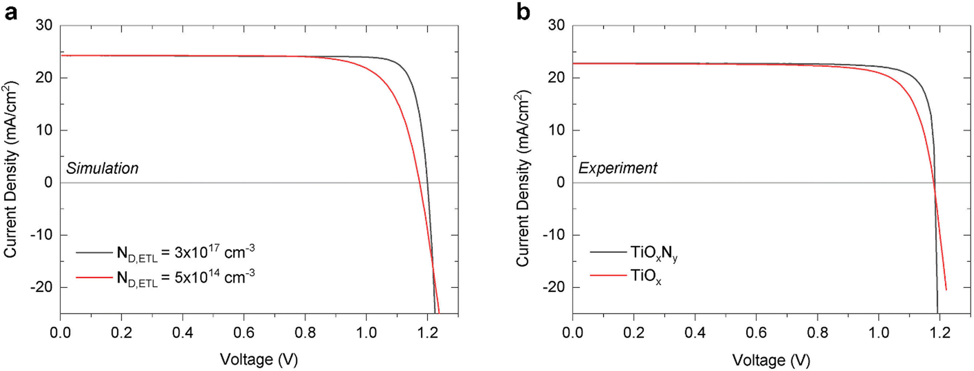 | ||
| Fig. 1 Comparison between simulated (a) and experimental (b) JV curves illustrating the performance improvement following the substitution of TiO2 for TiOxNy In the simulated curves of (a) only ETL doping is varied, taking ionised dopant densities from Hall effect measurements. Reduction in FF and increase in Ohmic series resistance is due to electron depletion in the ETL layer, a consequence of the space charge region of the ETL/TCO heterojunction. Reproduced from ref. 1. | ||
A FF on the order of 86% cannot be achieved unless all other factors of the PSC are highly performant. From this perspective, the lowly-doped, solution-processed TiO2 ETL was a significant bottleneck to performance. The experimental JV characteristics of the TiO2 and TiOxNy cells show that the FF difference is predominantly the result of higher series resistance in the TiO2-based cell, with negligible changes in open-circuit voltage, short-circuit current density or shunt resistance (Fig. 1). However, Hall effect measurements on the TiO2 film external to the PSC quantified conductivity at ∼10−4 S cm−1, for an Ohmic series resistance of ∼50 mΩ cm2 in a 50 nm thick film. At the maximum power point current of approximately 20 mA cm−2, the voltage loss contributed by this resistance is only ∼1 mV, while the experimentally observed difference was ∼80 mV. Thus, the ex situ conductivity cannot explain the restriction placed on FF and PCE, nor the gains realised with TiOxNy. Instead, an explanation that is consistent with these observations is the influence of the TCO layer on the electrostatics of the PSC itself, via a mechanism referred to in the wider thin-film solar cell literature as a “parasitic Schottky junction” (PSJ).2–5
A PSJ is the consequence of the work function difference, Δφ, between the TL and TCO. When in intimate contact, the materials exchange electrons until their Fermi levels are in equilibrium. Given the high dopant density of the TCO, the heterojunction forms an asymmetric space charge region that extends predominantly into the TL. Within the space charge region, majority carriers are depleted up to several orders of magnitude below the nominal density. With typical TL thickness of 50 nm or less, this space charge region can extend the full width of the TL and thus come to completely determine the conductivity of the TL once in place within a PSC. For the following discussion, we define the ex situ conductivity as the conductivity of the film outside of the cell, without the influence of the PSJ space charge region. Conversely, we define in situ conductivity as the conductivity when the TL is in place within the cell, with bulk properties determined by the electrostatic equilibrium of the perovskite–TL–TCO interface. In Fig. 2, we plot the simulated ex situ and in situ conductivity of a 50 nm-thick ETL as a function of dopant density, accounting for the influence of the TCO.
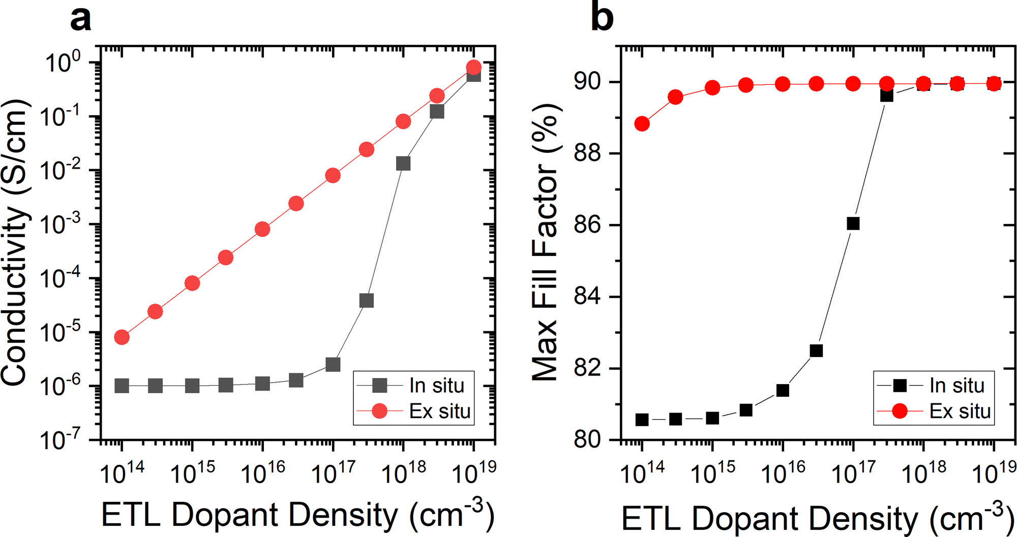 | ||
| Fig. 2 (a) Ex situ conductivity, calculated based on nominal doping density, and in situ conductivity calculated from the equilibrium carrier density at the maximum power point for each cell. At worst, the in situ conductivity is almost four orders of magnitude below the ex situ value. (b) Taking the in situ conductivity calculated in (a), the theoretical maximum fill factor for a 50 nm thick ETL with an electron mobility of 0.5 cm2 V−1 s−1 compared to a device where the ex situ conductivity is maintained once the ETL is in place in the PSC. | ||
The device modelling behind Fig. 2 we will describe in detail in the next section. For now, the key observations are that (1) for all TL dopant densities (ND) conductivity is reduced by the space charge region of the TL/TCO heterojunction, and (2) at lower values of ND, which for the set of parameters in this example is ≲1017 cm−3, conductivity is pinned at a very low level. This has two consequences. Firstly, if the ex situ conductivity of the TL is only marginally sufficient for a high FF solar cell, even a heavily doped transport layer (ND ≳ 1017 cm−3) may be sufficiently depleted to have a measurable impact on FF. This would occur along the range of dopant densities for which the in situ conductivity decreases rapidly as illustrated in Fig. 2b. Secondly, at low ND, the resistance of the TL once in intimate contact with the TCO can place an upper limit on FF. To compute this limit, we used an idealised one-diode equivalent circuit model, which presumes there are no other sources of (non-ideal) power loss in the cell. This computes an upper limit of FF of ≲83% (Fig. 2b). In other words, the in situ conductance of the 50 nm-thick TL is on its own sufficient to reduce FF by ∼7%, corresponding to an absolute efficiency loss of ∼2%. Critically, the cause would not be obvious based on ex situ measurements of the TL conductivity, which would suggest negligible resistance losses.
The influence of the Schottky junction, also referred to as the Schottky barrier, is a known loss mechanism in thin film solar cells and in the last two decades has received attention in the thin film and silicon heterojunction PV literature. Often, this work has focused on the impact of the energy barrier to charge transport, an energy penalty that must be surmounted for charge to flow, with a characteristic ‘S-shape’ to the JV curve. For example, in 2006 the TL/TCO Schottky barrier was called upon by Snaith and Grätzel to explain a low FF, S-shaped JV curve under monochromatic illumination in a dye-sensitized solar cell.3 In an early 2014 review, Green et al. computed an energy band diagram of a complete PSC, identifying an energy barrier to electron flow at the TiO2/FTO interface. However, it was suggested that the absence of obvious characteristics of an energy barrier indicated a smaller barrier in practice than predicted by idealised theory.6 Motivated by the observations of Snaith and Grätzel, one of the first PSC efficiency milestones from Zhou et al. in 20147 explicitly aimed to reduce the energy barrier with an ITO surface treatment prior to depositing TiO2. In 2014, Wojciechowski et al. proposed a low temperature fabrication process that maximised TiO2 doping, again with the intention of addressing in situ resistance.8 In 2015, Chen et al.9 doped a TiO2 layer with Nb to achieve a then record efficiency of 16.2%, recognising also the advantages for minimising PSJ losses. Beyond perovskite photovoltaics, simulations of the TCO heterojunctions in silicon heterojunction solar cells by Zhao et al.5 and Bivour et al.4 demonstrated that the space charge region of the TL/TCO structure could be detrimental to PCE via a reduction in FF.
Yet despite early attention in the PSC literature, in the years that followed only a small number of works explicitly referenced the PSJ and engineered PSC architectures to minimise associated losses.1,10–12 Furthermore, the theory of charge conduction in PSCs, exemplified by numerical device modelling, has almost completely ignored the TCO.13–16 One exception is a study from Sherkar et al, who observed a fill factor dependence on the energy barrier at the TL/TCO interface, but beyond the importance of the TL/TCO work function difference, did not consider the impact on bulk conductivity of the TL and how it may be mitigated.12 The fact that the impact of the PSJ in PSCs has hitherto not been rigorously quantified and characterised may explain why the phenomenon has faded from view, demonstrated by recent record PCEs that approach and exceed 25% but make no mention of this mechanism or explicitly attempt to address it.17–19
We develop a quantitative understanding of the PSJ in PSCs in the following section. One key observation from our analysis of the PSJ—which to our knowledge has not been quantified before in the perovskite literature—is the added influence the TCO can have on electrostatics and recombination within the perovskite layer itself. Where the TL contains insufficient space charge to fully screen the work function of the TCO, the accumulation of electric charge at the near-interface region of the perovskite is influenced by the TCO work function. Several theoretical studies, including our own, have shown that altering the distribution of ionic charge, and concurrently the distribution of electrons and holes, can influence rates of non-radiative recombination, which ultimately explains many manifestations of hysteresis in PSCs.13,15,20,21 In our theoretical exploration of the TCO's influence, we observed that the greater the influence of the TCO on the perovskite layer, the higher the rate of nonradiative recombination at any given defect density due to increased accumulation of minority charge carriers at the TL–TCO interface. This was consistent with our experimental observations in the substitution between TiO2 and TiOxNy,1 which showed an ∼8 mV increase in open circuit voltage. However, the magnitude of this voltage loss is conditional on the perovskite layer's ionic, dopant and recombination-active trap properties. Furthermore, this effect is diminished via bulk and interface passivation, while the TL conductivity loss is not. As a result, in this work we focus on the in situ conductivity losses. This is because the in situ resistance is particularly relevant for the highest performance cells to date, the performance of which suggests strong suppression of non-radiative recombination, exemplified by a recent 24.6% PCE with an open circuit voltage to band gap deficit of ∼300 mV described by Jeong et al.17 Nonetheless, the TCO work function can exacerbate non-radiative recombination in PSCs, and thus should be routinely included in device theory and modelling going forward, especially as TLs become increasingly thin and thus less able to screen the TCO from the perovskite layer.
Finally, PSJ theory suggests that the use of TiO2 transport layers in n–i–p cells may fundamentally limit FF in otherwise ideal PSCs. This is not the consequence of intrinsically low conductivity in TiO2. Early analysis of TiO2 films suggested that their amorphous structure severely limited conductivity, to levels as low as 10−8 S cm−1.9 However, higher conductivities, in the range of 10−6–10−4 S cm−1 are now regularly reported in TiO2 films with and without additives.7–9,22–27 According to the idealised calculations using equivalent circuit modelling (Fig. S1, ESI†), conductivity >3 × 10⁻⁶ S cm−1 predicts negligible series-resistance losses in 50 nm-thick layers. This then begs the question as to why the highest certified FF on solution-processed or spray pyrolysis TiO2 is still only 81.8% as recently reported by Jeong et al.,19 despite significant optimisations in all other aspects of the PSC structure. Indeed, breakthroughs in certified FF have only occurred in n–i–p PSC structures following the move away from TiO2 ETLs. From the perspective of PSJ theory this may be the consequence of a low intrinsic ionised dopant density (<1016 cm−3) in some TiO2 layers, as suggested by several studies,10,24,26,28 for which electron depletion due to the PSJ will be enough to reduce in situ conductivity by several orders of magnitude (Fig. 2). Continued use of such TiO2 films would then require thicknesses <20 nm to ensure negligible FF losses, which can be challenging to achieve with high conformality.
This study therefore emphasizes that by ignoring the electrostatics of the TL/TCO structure, relatively facile efficiency gains—primarily through reduced series resistance and improved FF—may be going unrealised even in state-of-the-art PSC devices. In addition, where structural changes may have mitigated the PSJ to some extent this factor is not recognised, which may lead to misdirected efforts in optimisation. In the following sections, we begin by describing the physics of the PSJ, its characteristic manifestation in the current–voltage (JV) curves of PSCs, and the key material properties that influence the magnitude of the in situ conductance. With reference to original numerical, electronic–ionic device simulations and treatments elsewhere in the thin-film solar cell literature, we discuss relatively straight-forward methods for mitigating PSJ power loss. Subsequently, we consider three groups of experimental data that suggest that PSJ losses may be more prevalent than is fully appreciated: (1) the correlation between ETL material and certified FF records in n–i–p PSCs, (2) a direct comparison between two recent certified small area device records ∼25%, and (3) evidence of ETL depletion from cross-sectional KPFM profiles. To broaden the scope of our analysis, we will conclude by discussing the implications of the PSJ for inverted PSC structures, for which the HTL is the sunward transport layer in contact with the TCO. We consider the extent to which this may explain the generally higher FFs reported on these structures coupled with low open circuit voltages. Ultimately, we make the case that minimising in situ resistance due to the PSJ will be essential to raise single junction PCEs beyond 26%.
Physics of the TL–TCO heterojunction
The influence of mobile ionic defects and hysteresis
The simulations of this work were performed in COMSOL Multiphysics, which simulate all device layers in bulk, including the TCO, using an ionic–electronic semiconductor drift diffusion model as previously described.15,20 These simulations include two mobile ions (anions and cations) of equal concentration. The JV simulations are transient in the reverse direction, with a voltage scan rate of 0.1 mV s−1, chosen to reflect a quasi-steady state (QSS) measurement protocol in which the ions are at steady state at each point in the JV curve. This avoids the influence of JV hysteresis on FF but does capture the influence of the rearrangement of the mobile ion population as the cell moves along the JV curve. In addition, it reflects both the standardized QSS measurement protocol for PSC certification, and practical operating conditions, which stabilize about the maximum power point.We observed that ion concentration in the perovskite absorber had a small influence on PSJ loss in the ETL and the resultant FF, relative to key factors such as ETL dopant density, and the TL/TCO work function difference as we will describe in the next section. The influence of ion concentration and ETL dopant density on FF is presented in the contour plot of Fig. S2 (ESI†). A greater ion concentration (>1017 cm−3) can improve FF by up to approx. 2–3% abs. at any given ETL dopant density. However, in the same device, an increase in ETL dopant density, which reduces PSJ losses, can increase FF by up to 12% abs. at any given mobile ion concentration. Any practical quantity of mobile ions is thus unable to explain, or fully recover, the FF losses due to the PSJ.
Beyond the influence of ions on PSJ FF losses, the rate of non-radiative recombination in a PSC is affected by ion migration in the perovskite absorber.13,14,20 In effect, recombination ‘sensitizes’ the JV characteristics to the movement of ions during the JV scan (among other measurements). However, our device simulations set a low concentration of non-radiative recombination active defects in the perovskite bulk and at the perovskite-transport layer interfaces in order to simulate a high-performance PSC (i.e. Voc ≈ 1.24 V with perovskite bandgap of 1.60 eV). Therefore, our simulations do not predict FF loss due to the influence of ion migration on non-radiative recombination. Instead, our simulations represent high performance, low-hysteresis PSCs and isolate the impact of the PSJ on an otherwise near-lossless device. Given these factors, the following analysis does not consider the influence of mobile ions further, and all simulations use a consistent ion concentration.
The electrostatics of the TL–TCO heterojunction
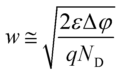
An in situ reduction in TL conductivity induced by the parasitic Schottky junction (PSJ) is driven foremost by the work function difference between the TL and the TCO, Δφ. For this discussion we refer to the resistivity introduced by the space charge region of the PSJ as the in situ resistivity (ISR). For clarity, and for its relevance to our analysis of the efficacy of TiO2 as an electron transport layer (ETL) we will focus on a “standard” n–i–p perovskite/ETL/TCO structure and will return to inverted structures later.In a standard structure, the TCO and the ETL form a heterojunction due to the difference in their work functions, Δφ. The magnitude of Δφ depends on the TL–TCO materials and the chemistry of the interface formed between them. Although a function of the dopant density, TiO2 ETLs have work functions on the order of 4.0–4.4 eV,9,29–31 and for SnO2 approximately 4.5 eV,32,33 while fluorine-doped tin oxide (FTO) and indium-doped tin oxide (ITO) materials have work functions that span the range of 4.4–4.8 eV.34,35 Consequently, we can expect Δφ to range up to 800 meV, although the plausible range is constrained by practical requirements for effective charge transport. As we will see, magnitudes of Δφ < 250 mV can be sufficient to introduce significant ISR. If the TCO work function exceeds that of the ETL, electrons flow from the ETL to the TCO to reach equilibrium, depleting majority charge carriers within the space-charge region of the ETL. In a Schottky-type heterojunction, the high electron density of the TCO means that it cannot sustain net charge in its bulk, resulting in an asymmetric junction in which the space charge falls entirely on the ETL side. Under many configurations of the junction, the space charge region will extend the full width of the ETL. The thickness of this region in the ETL, w, is approximated by
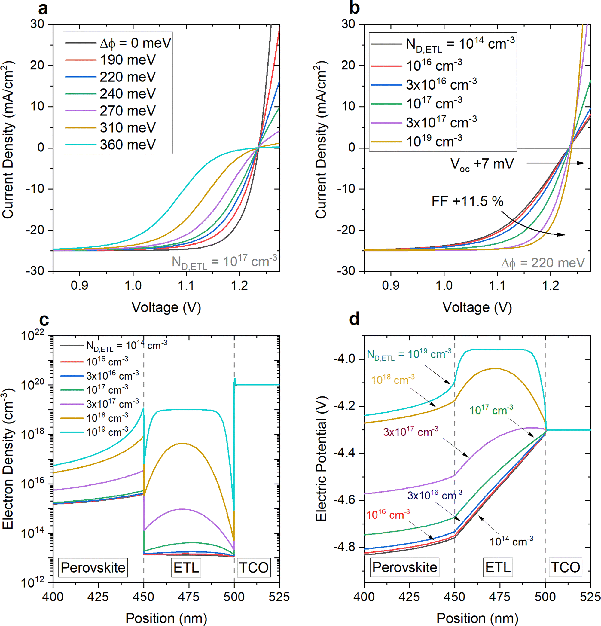 | ||
| Fig. 3 (a) Simulated JV curves as a function of the work function difference between the ETL and ITO layers, Δφ, where ND,ETL = 1017 cm−3. (b) Simulated JV curves as a function of ETL doping when Δφ = 220 meV (defined when ND,ETL = 1017 cm−3). Heavier doping mitigates against electron depletion from the ETL, recovering both voltage and FF. Note truncated x-axis range in (a) and (b), to emphasize differences in the JV curves. (c) Simulated electron density as a function of ETL doping at the maximum power point of the JV curves plotted in (b). Dashed lines show nominal electron density based on ETL dopant density/conductivities calculated from these profiles are presented in Fig. 2a. (d) Simulated electric potential profile across the ETL layer as a function of ETL doping under semiconductor equilibrium conditions, i.e. without illumination or applied bias. | ||
At a fixed ETL dopant density, as Δφ increases from zero (and w expands), the series resistance component of the JV curve increases, and FF and PCE decrease. Then, above a threshold value, which in this example is approximately Δφ = 250 meV, the energy barrier at the TL/TCO interface is sufficient to introduce a clear s-shape to the JV curve. Clearly, we do not see s-shaped curves in well-performing devices. However, the critical observation is that below the “s-shape threshold” there is an intermediate range of Δφ where the JV curves simply exhibit non-zero levels of series resistance, but there is no direct evidence that ISR losses are responsible. Suboptimal TCO/ITO junction properties are therefore not a binary condition, revealed by the presence or absence of an S-shaped JV curve. That ISR losses can occur in this manner may explain why focus on the PSJ has faded in recent years. There are, after all, many possible sources of series resistance in a solar cell.
Because we are interested in cells with resistance losses within the intermediate range below the s-shape threshold, we now take a closer look at a cell in which Δφ = 220 meV (blue curve, Fig. 3a). To illustrate how increasing ND mitigates ISR in the TL, we plot simulated JV curves for a range of ND in Fig. 3b, holding TCO work function constant. The quasi-steady state electron density at the maximum power point of these curves is presented in Fig. 3c. The corresponding equilibrium electric potential profiles, or the relative position of the electron Fermi level, are plotted in Fig. 3d. The relevance of the latter data will be revealed when we consider experimental contact potential difference profiles as evidence of ISR in the next section.
As shown in Fig. 3b and c, ND is a critical factor because it determines the density of ionized dopant defects, which constitute the space charge that screens the ETL bulk (and ultimately, the perovskite) from the work function of the TCO. For Δφ = 220 meV, it is only when ND = 1019 cm−3 that there is sufficient space charge density in the ETL to completely screen the ETL bulk from the TCO, such that the ETL bulk carrier density is unchanged from the nominal value. We note that as ND increases, the Fermi level in the TL rises toward the conduction band minimum, which will increase Δφ. However, our simulations demonstrate that the net change in conductivity is positive with increasing doping. That is, within a limited range of Δφ, the increased TL/TCO energy barrier from increasing ND does not introduce significant resistance to electron flow.
Below ND = 1019 cm−3, the space charge region extends deeper into the TL and the magnitude of electron depletion increases. In this example, for ND > 1017 cm−3, although the free electron density falls below ND, there is still sufficient equilibrium concentration that ISR losses are small, and FF reductions modest. Below 1017 cm−3, however, the low equilibrium electron concentration reduces fill factor significantly, as illustrated in Fig. 2. The ISR thus introduces a disproportionately large performance penalty on ETL materials with low dopant density for any given value of Δφ. The aggregate effect on PCE is captured in Fig. 3b. Electron depletion substantially increases resistance in the ETL and as previously observed, increases rates of non-radiative recombination in the perovskite layer by altering charge accumulation at the perovskite/TL interface. The sum of these effects predicts that across an ETL dopant density of 1014 to 1019 cm−3 FF and PCE can rise by up to approx. 11.5% and 3% absolute, respectively. Although the ex situ conductivity of the TL predicts a small contribution to series resistance, the ISR can lead to a ‘hidden’ source of FF loss that only manifests once the ETL is integrated into the device.
As per the preceding discussion, there are three clear approaches to mitigating ISR: (1) reduce Δφ, (2) increase ETL dopant density, (3) reduce ETL thickness or (4) employ ETL materials with high mobility. The work function difference, Δφ, may be the most difficult to control. The energy barrier that forms in practice between two materials is often determined by interface states that are a product of the two materials and the method of preparation, and are difficult to predict or control a priori.36 Nonetheless, transport layer materials with work functions that are closer to that of ITO or FTO are more likely to exhibit smaller work function differences. As we will discuss in more detail in the next section, this favours for example SnO2 as an ETL material, relatively to TiO2. On the other hand, TCO materials with shallower work functions could reduce Δφ. One example is Zr-Doped Indium Oxide (IZRO), with a reported work function of 4.2 eV.37
Increasing dopant density will also maintain lower ISR for any given value of Δφ, and high doping density TL materials with suitable band alignment vis-à-vis the perovskite absorber, such as SnO2 and TiOxNy, have already been demonstrated in the literature.28,38 As evidence for the efficacy of increasing ND in silicon heterojunction solar cells, Bivour et al. found that increased boron doping of a p-type amorphous silicon transport layer improved FF up to 4% absolute.4 ISR losses have not received ongoing attention in silicon heterojunction photovoltaics, which may be explained by the naturally heavy doping of amorphous and poly silicon, which is typically at the solid solubility limit ≳1020 cm−3.39
Reducing thickness of the TL will reduce the total resistance for any given conductivity, hence mitigating FF losses. The idealised equivalent circuit simulations of Fig. S1 (ESI†) show that for an ETL layer with an in situ conductivity of 10−6 S cm−1, reducing thickness from 50 nm to 20 nm improves the FF potential of the cell from ∼81% to ∼87%, for a gain of approximately 2% (abs) per 10 nm reduction in thickness. However, it is challenging to reduce thickness in solution-processed films such as TiO2 while avoiding pinholes that increase interface recombination and introduce shunts via direct contact between the perovskite and TCO layer.40 This may favour materials or methods of deposition that can produce conformal coverage at very low thicknesses. Furthermore, if using lowly doped ETLs and attempting to mitigate series resistance via a thinner layer, control of thickness will be critical. As previously observed, every 10 nm increase in thickness reduces FF by 2% abs. or PCE by approx. 0.6% abs. This will reduce the degrees of freedom in cell fabrication and may challenge high-throughput industrial manufacturing. By comparison, these fine tolerances will not be present for more heavily doped TLs. Nonetheless, the proven track record of stability and easy integration of TiO2 films into high efficiency PSCs suggests that deposition methods suitable for sub-20 nm thick films may be worth pursuing.
A sufficiently large majority carrier mobility can also overcome low ISR. Our previous simulations used an ETL electron mobility of 0.5 cm2 V−1 s−1, within the typical range quoted for TiO241 and equivalent to that measured in our TiO2 and TiOxNy films. Yet, as the critical property is the total in situ resistance of the transport layer, a larger majority carrier mobility will reduce the ISR for any given magnitude of TL depletion. As an example, in Fig. S3 (ESI†) we plot the achievable fill factor as a function of ETL dopant density and mobility using the idealised equivalent circuit model of Fig. S1 (ESI†) (Δφ = 220 meV). An ETL mobility >3 cm2 V−1 s−1 results in an upper bound on FF of at least 88%—all other factors being equal—relative to approx. 80.5% for a mobility of 0.5 cm2 V−1 s−1. However, the reduction in ISR due to higher mobility can be partially undone by an increase in Δφ, which results in a lower equilibrium electron density (i.e. greater depletion). To quantify this effect, Fig. S4 (ESI†) plots the JV curves and corresponding fill factor for a device in which the ETL electron mobilities are 3 and 100 cm2 V−1 s−1 and ND,ETL = 1017 cm−3. The latter mobility is at the upper end of values measured for PSC-compatible ETL materials.42 Yet even in this case, an increase in Δφ to 320 meV (the approximate threshold at which an s-shape characteristic appears in the JV curve) still produces a fill factor loss of approx. 4% abs. A higher mobility reduces ISR FF loss but does not eliminate the possibility entirely. The broader interdependence of Δφ and ETL mobility on FF is captured in the contour plot of Fig. S5 (ESI†), which illustrates how larger values of Δφ can partially reverse the FF gains of higher ETL mobility. Nonetheless, higher transport layer majority carrier mobility is desirable under any circumstances, which favours ETL materials such as ZnO and SnO2, as we will discuss in the next section.
To conclude this discussion of the PSJ, we consider the other side of the interface: the perovskite–ETL junction. At this interface a heterojunction is formed that can also deplete majority carriers from the ETL. This is a result of the (quasi-)Fermi level for electrons being below that of the ETL, particularly if the perovskite is p-type. In our simulations, we found that electron depletion in the perovskite layer had a smaller impact, relative to the work function difference with the TCO. The impact of the ETL-perovskite heterojunction alone is implicitly demonstrated in the simulated JV curve for Δφ = 0 meV (black curve) in Fig. 3a. This magnitude of Δφ results in negligible electron depletion from the ETL to the TCO, and total FF is predicted to be ∼88%. However, the relative magnitude of these losses is conditional on the perovskite properties, e.g. fixed dopant density, ion concentration, band gap and electron affinity. It is also impacted by the injection level within the perovskite, which determines the quasi-Fermi level for electrons, the exploration of which are beyond the scope of this study.
Evidence for ISR power loss
In the preceding section, we laid out the theoretical basis for the parasitic Schottky junction (PSJ) in a perovskite solar cell. We identified an intermediate range of PSJ-induced TL depletion that increases series resistance and reduces FF without the characteristic s-shaped JV curve that is symptomatic of high energy barriers to charge carrier flow. Now, we consider evidence from the literature, both direct and circumstantial, that ETL depletion may be occurring in even state-of-the-art n–i–p PSC structures.Power losses due to ISR may be apparent in the historical trend in certified FFs from state-of-the-art PSCs. In Fig. 6, we plot the FF taken from both certified efficiency records reported in the solar cell efficiency tables and other notable certified JV measurements, all of which were recorded on an n–i–p structure.43 Between 2017 and 2019 FF plateaued at approximately 80%, even as open circuit voltage continued to improve. After 2019, FF increased stepwise by roughly 4% absolute and has continued to improve by over 6% absolute with our result in late 202128 (Fig. 4). Clearly, there are many structural and compositional differences between these cells. However, one change correlated with the step change in FF is a shift from TiO2 to tin oxide (SnO2) and eventually TiOxNy, as the ETL material. This invites the question as to whether the improvement in FF from TiO2 to SnO2 is due to the same reduction in ISR we observed with the TiO2 to TiOxNy substitution. Measurements of TiO2ND < 1016 cm−3![[thin space (1/6-em)]](https://www.rsc.org/images/entities/char_2009.gif) 1,10,26,44 could make TiO2 highly susceptible to ISR, limiting FF to the low 80 s in otherwise high-performance cells (Fig. 2). This is consistent with the plateau in certified fill factors around 80%. Indeed, if we consider progress in TiO2-based PSCs since 2019, certified FFs have still only reached 81.8%, in this case in a device that currently matches the world record in certified PCE of 25.2%,19 indicative of extremely high performance in all other factors of the cell.
1,10,26,44 could make TiO2 highly susceptible to ISR, limiting FF to the low 80 s in otherwise high-performance cells (Fig. 2). This is consistent with the plateau in certified fill factors around 80%. Indeed, if we consider progress in TiO2-based PSCs since 2019, certified FFs have still only reached 81.8%, in this case in a device that currently matches the world record in certified PCE of 25.2%,19 indicative of extremely high performance in all other factors of the cell.
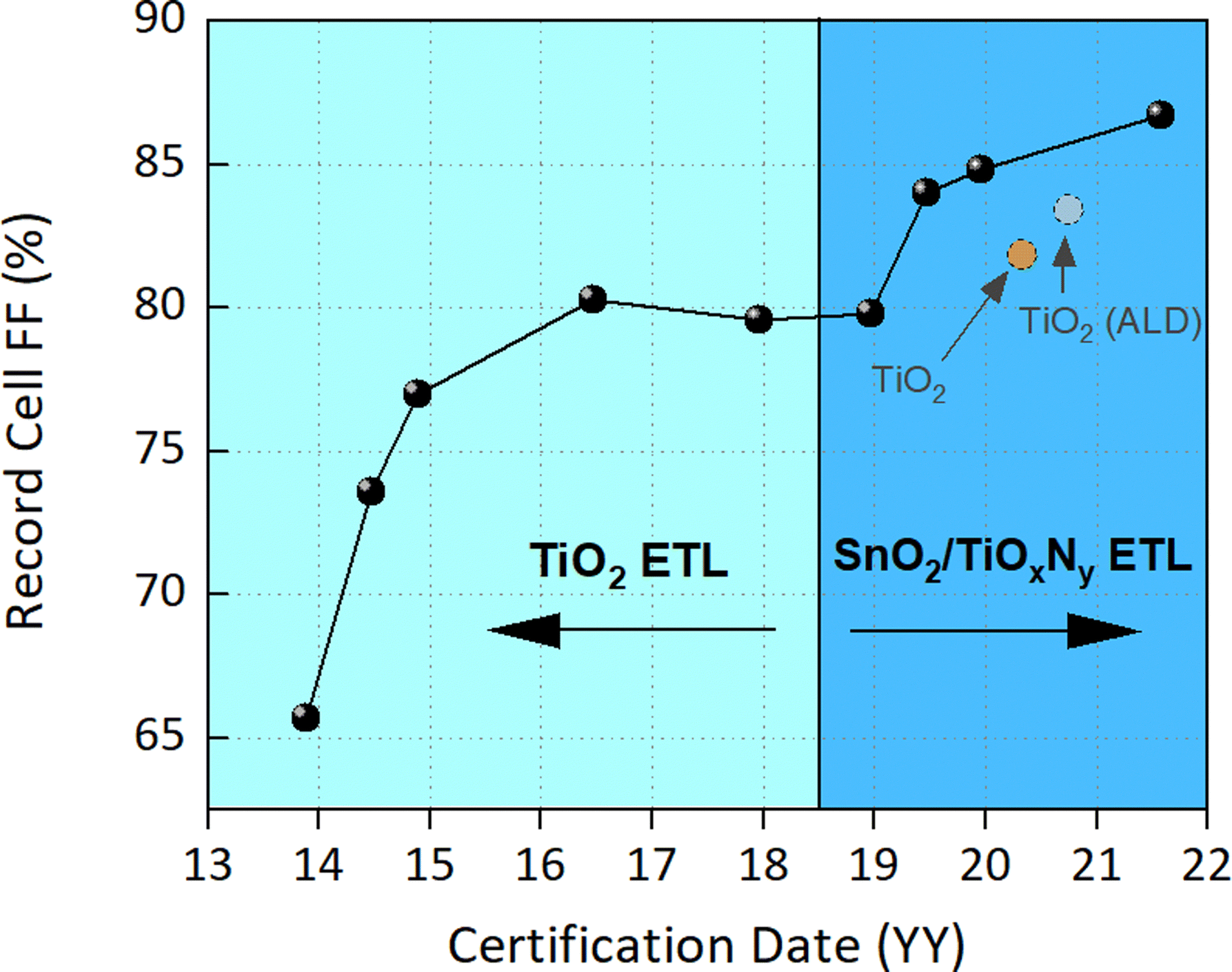 | ||
| Fig. 4 (a) Certified FFs taken from efficiency tables and other notable certified results, published according to the date of certification.18,75–79 All cells are n–i–p structures, and the transition from TiO2 to SnO2 and TiOxNy ETL materials coincides with a step-change increase in FF. The certified result from ANU, plotted independently, was fabricated on ALD TiO2, for which we have measured doping levels in the range of 1017–1019 cm−3.54 Also plotted is the current certified record FF for a PSC fabricated on non-ALD TiO2.19 | ||
From the perspective of ISR, SnO2 offers several advantages over TiO2. Foremost, measured dopant densities, with and without additives, are consistently in the range of 1017 to 1018 cm−3,27,45,46 of a similar magnitude to TiOxNy. In addition, SnO2 is often deposited at thicknesses ≤30 nm45–47 and electron mobility is reported to be as high as ∼200–400 cm2 V−1 s−1.48,49 The larger work function of SnO2 also reduces the possible magnitude of Δφ. Thus, in minimising ISR, SnO2 is advantaged along several dimensions: heavier doping results in a higher in situ equilibrium electron concentration (Fig. 3c), while lower thickness, higher electron mobility and a deeper work function relative to TiO2 greatly increases the likelihood of low in situ resistances to a level that could pose no fundamental restriction on overall FF.
An interpretation, therefore, of the global trend in certified FF presented in Fig. 4 is an unrecognised mitigation of PSJ resistive losses in the ETL of n–i–p PSC structures, achieved by a transition from TiO2 to SnO2. As further evidence, we consider in detail two recent certified efficiencies on small area cells. In late 2020, Jeong et al. reported a PCE of 24.6%, on a low-bandgap dual cation perovskite17 with a remarkable ∼300 mV bandgap to open-circuit voltage deficit. The reported voltage is more than 98% of the Shockley–Queisser limit for the given bandgap energy and indicates that non-radiative recombination in the device is extremely low, both in the perovskite bulk and at the interfaces. Optimization of the HTL material maximised PCE primarily through improved FF. Despite this, the certified FF, at 79.7%, is ∼10% absolute below the theoretical limit for the measured voltage. If non-radiative recombination cannot explain this deficit, and HTL optimisation reduces the likelihood that the positive terminal is contributing significant FF loss, we are left to propose other sources. The characteristic of the JV curve for this cell (Fig. 5) is consistent with significant series resistance (compare with Fig. S1, ESI†). One candidate is Ohmic resistance in the TCO. However, the cell area is approximately 3 × 3 mm2, which predicts a relative (not absolute) PCE loss of at most 1% in the FTO layer, presuming a sheet resistance of 10 Ω □−1 using the analytical model of Jacobs et al.50 We then consider the negative terminal: the cell was fabricated on an FTO substrate with a spray pyrolysis deposited TiO2 ETL. As we previously discussed, a low TL dopant density and the predicted range of Δφ may make this TCO/TL structure susceptible to high ISR. Therefore, a plausible explanation for the unusually low FF relative to the open circuit voltage is the ISR of the TiO2 layer, with maximum power point resistive voltage losses exacerbated by the high (∼26 mA cm−2) photocurrent.
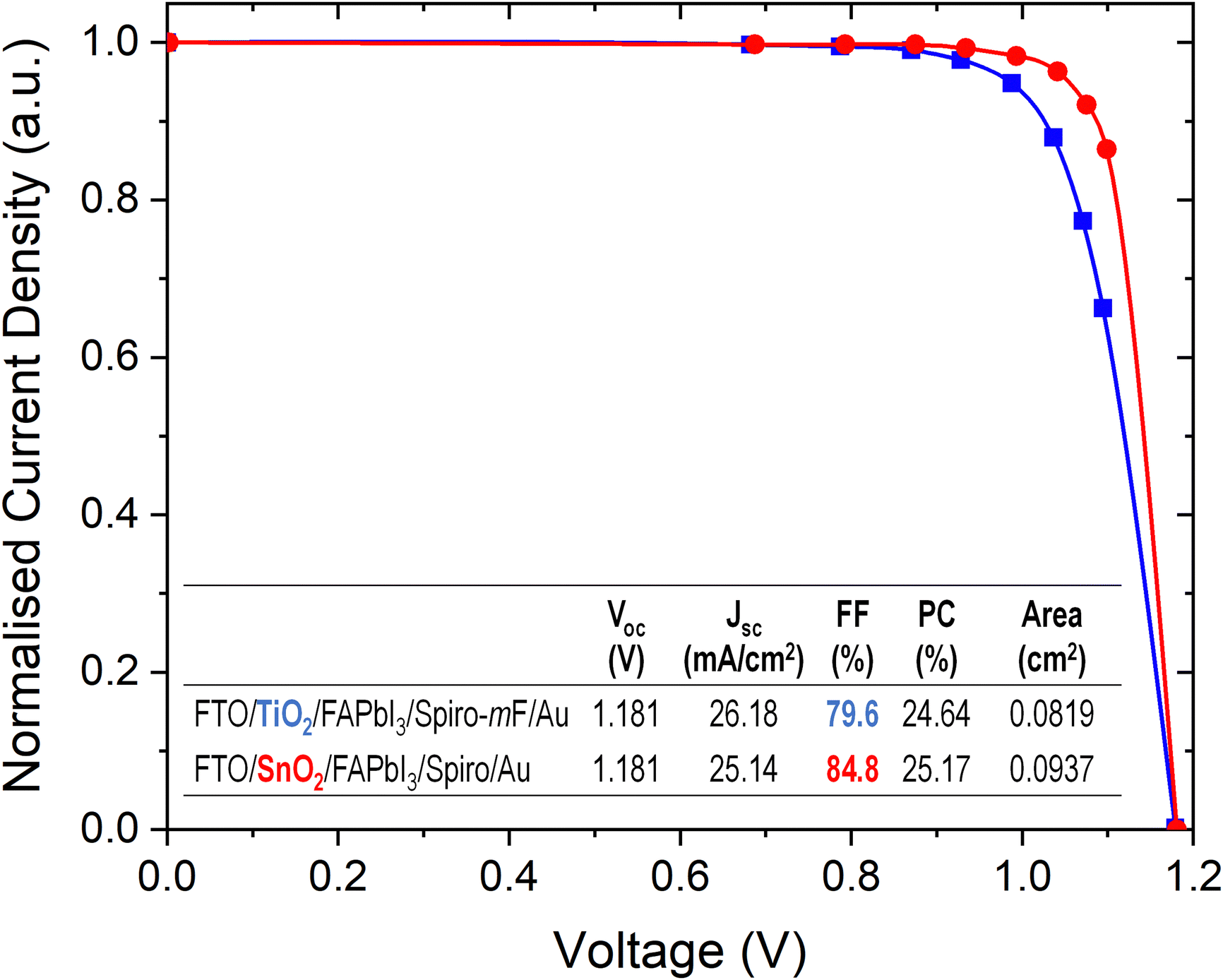 | ||
| Fig. 5 Certified QSS JV data of champion cell from Jeong et al.19 and Yoo et al.18 Data has been digitized and current density normalised for direct comparison. The gradient of the voltage/current relationship between Vmpp and Voc (∼1000–1180 mV) is indicative of non-ideal series resistance. The cell of Jeong et al. is fabricated on an FTO/TiO2 substrate, which our analysis suggests may be highly susceptible to power loss due to the TCO/ETL parasitic Schottky junction. By comparison, the certified performance from Yoo et al. has achieved a FF 5% absolute greater on a structure based on a FTO/SnO2 interface. | ||
A comparison to a more recent report by Yoo et al.18 illustrates the magnitude of the ISR power loss that may have occurred in the cells of Jeong et al. Yoo et al. achieved a certified small area efficiency of 25.2%, in which a key structural change was SnO2 as the ETL. This cell had a lower photocurrent (25 mA cm−2), and a higher voltage to bandgap energy deficit (389 mV with aperture mask) than Jeong et al. yet reported a larger certified FF by 5.2% absolute. The improvement in PCE was thus entirely a result of improved FF. A comparison of the JV curves (Fig. 5) shows that this improvement was driven by a reduction in series resistance. The SnO2 layer—which was optimised to maximise doping density as indicated by UPS data—may therefore be the source of this gain through minimizing ISR. Although Yoo et al. ascribed much of the performance enhancement to improvement of the conductivity and conformality of the SnO2, they did not consider the possibility that PSJ losses were being mitigated. Conversely, Jeong et al. may have fabricated a highly efficient device constrained by resistance losses in the ETL, as with control samples in our recent work before the incorporation of TiOxNy. If we just consider the ex situ conductivity of TiO2 compared to SnO2, we do not predict the magnitude of FF increase between these two structures. A straight-forward calculation shows that if a more heavily doped ETL layer (≥1017 cm−3) were incorporated into the cell structure of Jeong et al. to achieve FF on par with the certified value from our recent device (>86%), while maintaining the outstanding open-circuit voltage and photocurrent, then PCE would comfortably exceed 26%. This would put perovskite solar cell performance on the same level as the current record in silicon solar cells.51 TL ISR may therefore be one of the last major unrecognised sources of significant power loss in state-of-the-art PSC structures.
Before we continue to our final line of evidence of ISR losses in the PSCs, we note that Mott–Schottky measurements of TiO2 have suggested that the ionised dopant density may be on the order of 1019 cm−3,2,52 for which our theoretical treatment predicts low ISR. The wide range of reported ionised dopant densities in TiO2 films may be a function of how the material is fabricated.53 Notably, we have previously quantified via Hall effect measurements an ionised dopant density in ALD-processed TiO2 in the range of 1017–1019 cm−3.54 This material we incorporated into a 1 cm2 PSC, which recorded a certified FF of 83.9%.55 However, beyond direct measurements of TiO2ND < 1016 cm−3,1,10,26 there are indirect indications of low ionised dopant density in TiO2 materials used in PSCs. First is a series of injection-dependent conductivity measurements of TiO2 performed by Leijtens et al.24 using pulsed laser excitation. These data showed a strong injection-level dependence of conductivity and mobility in TiO2 across a carrier density range of ∼2 × 10¹⁶–3 × 1017 cm−3, which is inconsistent with an intrinsic dopant density >1019 cm−3. This was observed for TiO2 materials with and without conductivity-enhancing additives.
The second line of evidence of low ionised dopant density in TiO2 comes from data that also suggest heavy electron depletion and increased ISR in TiO2 ETLs more generally. These data are cross-sectional contact potential difference (CPD) profiles measured using Kelvin force probe microscopy (KPFM) techniques, which we interpret with the aid of the simulated electric potential profiles of Fig. 3d. CPD measurements capture the spatial distribution of the relative surface potential across a perovskite solar cell with high spatial resolution. Cross section KPFM measurements are technically challenging, but in recent years several groups have published high resolution CPD profiles of complete PSCs.56–60 These data provide arguably the clearest view into charge distribution in PSCs, and as they capture the potential profile across full devices can reveal the equilibrium distribution of electric charge, and hence the in situ space charge within the ETL.
CPD profiles taken from TiO2/perovskite/spiro PSCs are presented in Fig. 6. These profiles show, in principle, the relative position of the local work function (WF) as the Kelvin probe scans across the cell cross-section, although we must assume that the surface potentials are uniformly indicative of the bulk potential across all layers. By comparing the gradient of the CPD across the TiO2 layer to the simulated profiles of Fig. 3d, we see that the shallow (quasi-linear) curvature of the profile across the TiO2 layer in all measurements is consistent with low space charge density, ρ, and hence low ND (as per Gauss’ law, ∇2V = −ρ/ε). Per the simulated electric potential profiles, if the TiO2 were doped ≥1018 cm−3, we expect to see an exposed space charge density capable of screening the TiO2 bulk from TCO work function, and hence a bulk potential in the TiO2 layer that lies closer to the intrinsic work function. As presented, the CPD profiles are instead consistent with the simulated profiles where ND < 1016 cm−3. In addition, the measured profiles are consistent with the space charge region extending the full width of the TiO2 layer, with implications for bulk non-radiative recombination as discussed in the previous section.
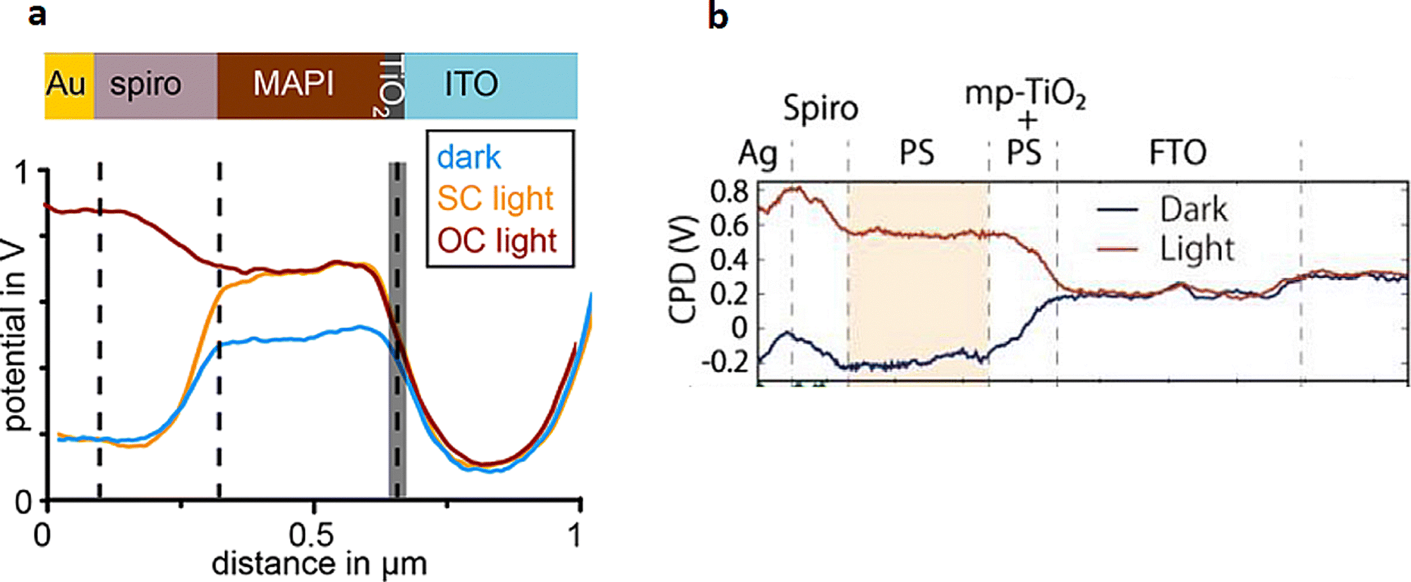 | ||
| Fig. 6 Contact potential difference profiles take from KPFM measurements of PSC cross sections. In both cases, the electric potential across the TiO2 layer is consistent with low ionised dopant density and significant depletion from the TiO2 layer (compare to simulation results of Fig. 3d). (a) Reprinted with permission from Hermes et al., J. Phys. Chem. Lett. 2018, 9 (21), 6249–6256. Copyright 2018 American Chemical Society,58 (b) Reprinted from Cai et al.57 | ||
Implications for inverted PSCs
The preceding discussion of n–i–p PSCs has suggested that the PSJ in a TiO2/TCO layer structure may introduce series resistance that places a fundamental limit on FF, which is circumstantially consistent with historical trends in the certified state-of-the-art performance records in n–i–p PSCs. The obvious comparison is inverted structures, which have repeatedly reported uncertified FF > 84%61–64 with at least two reports of FF ≥ 86%.63,64 As seen from the perspective of PSJ theory, a key difference between standard and inverted structures is the material that contacts the TCO.In inverted structures, majority charge carriers can also be depleted from the TCO-adjacent hole transport layer and consequently there is the same dependence on doping density (NA), Δφ and thickness to mitigate ISR losses. A common HTL for inverted PSCs with FF > 84% is PEDOT:PSS.61–63 The doping density, NA, of PEDOT:PSS typically exceeds >1019 cm−365 and thickness is approximately 40 nm. The work function of PEDOT:PSS at 4.7–5.4 eV66 predicts a similar magnitude (although opposite sign) of Δφ as compared to TiO2/TCO structures, up to 1.0 eV. Beyond PEDOT:PSS, a notable recent FF of 86.2% is described by Cao et al.64 on a 20 nm NiOx HTL. Although dopant densities and hence work function vary with preparation method, NiOx has been reported with doping densities in the range of 1016–1019 cm−3,67 and a work-function ∼5.0 eV.68 These HTL materials benefit from reduced thickness and increased ionised dopant density, relative to the TiO2/TCO structure in n–i–p PSCs. Consequently, inverted cells may have generally achieved higher FF due to widely used HTL materials being both comparatively thin and heavily doped relative to TiO2, mitigating the ISR.
In this context, it is interesting to note that while inverted cells have achieved FFs greater than n–i–p PSCs, the open circuit voltage and hence PCE is typically lower. For example, Chiang et al.63 reported 86% FF with 1060 mV Voc, Wu et al.62 reported 85% FF and 1030 mV Voc, while the recent 86.2% FF of Cao et al.64 achieved a comparatively modest 1120 mV Voc. In each case, low voltages reduced overall solar cell efficiency. An explanation for the counter-intuitive correlation between FF and open circuit voltage comes from PSJ theory. Firstly, however, we must recognise that FF is a function of both the open circuit voltage and the short circuit current density and the voltage and current density at the maximum power point. In our simulations, we observed that if most non-radiative recombination takes place at a TL interface, then the reduction in maximum power point and open circuit voltage is approximately proportional over a wide range of interface defect concentrations (Fig. 7). In addition, there is minimal influence on the internal quantum efficiency and short circuit current. Consequently, the open circuit and maximum power point voltages fall due to increased recombination, while fill factor remains relatively unchanged.
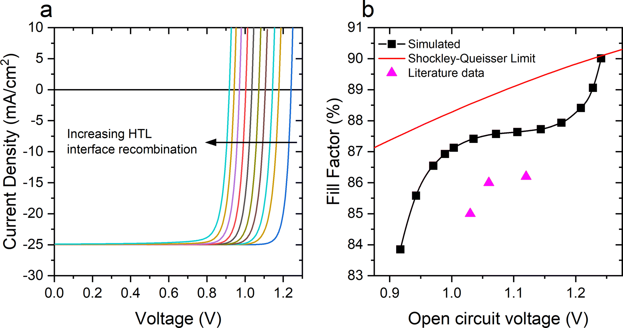 | ||
| Fig. 7 Simulated FF potential for a PSC in which only non-radiative recombination is the limiting factor on performance (i.e. no majority carrier depletion and increased ISR in TL). (a) Simulated JV curves vs. an increasing density of recombination-active (midgap) defects at the HTL interface. (b) FF as a function of the open-circuit voltage, extracted from the simulated JV curves of (a). The FF varies by only 0.5% abs. between open circuit voltages of 1.0–1.2 V due to the approximately proportional reduction in Voc and Vmpp as HTL interface defect density increases. The nuance of the relationship between Voc and Vmpp is beyond the scope of our discussion here. Instead, these results demonstrate that relatively low voltage is compatible with high FF so long as there is high charge carrier collection efficiency, e.g. by avoiding TL series resistance induced by the PSJ. Literature data on Voc-FF in inverted cells are plotted alongside simulated data.62–64 The relationship between voltage and FF are suggestive of very low resistance losses, including PSJ losses in these inverted cell architectures. | ||
However, for high FFs to be achieved under low voltages, charge transport resistance across the whole device must be very low. Resistance within the perovskite bulk is expected to be minimal, owing to high perovskite diffusion lengths relative to the absorber thickness, which is suggested by multiple measurements of the electronic quality of perovskite films.64,69,70 Indeed the 86.2% FF of Cao et al. was supported by optimisation of electron and hole mobility in the perovskite layer. In addition, resistance in the transport layers must also be very low. Hence, meaningful ISR would make the combination of low open circuit voltage and high FF extremely difficult to achieve.
To test this notion, we simulated the JV characteristics of a PSC in which high TL doping (NA = 1019 cm−3) and high perovskite mobility (μe = μh = 15 cm2 V−1 s−1 as per Cao et al.) ensured negligible resistance losses in the cell, most notably the absence of HTL ISR. We varied recombination at the perovskite–HTL interface by adjusting the interfacial recombination-active defect density. As recombination increased and voltage fell, the theoretically achievable FF remained relatively constant at ≳87% across a range of Voc from 1000–1200 mV (Fig. 7). The nuances of the injection-dependent recombination dynamics are beyond the scope of our discussion, but these simulations nonetheless illustrate that FF ≳ 87% can be achieved in PSCs with voltages as low as 1000 mV, provided no other sources of resistive power loss are present. Therefore, the combination of high FF and low voltage in inverted cells is evidence that these structures are less susceptible to TL ISR losses.
Finally, we must acknowledge that all the calculations in this work have assumed that resistive power losses at the dark side of the cell are very low. In principle, the Schottky junction that can lead to majority carrier depletion at the TL–TCO interface can also occur at the metalized side of the PSC. Referring to the FF gains from the incorporation of TiOxNy, cell performance suggests that in this structure resistance losses introduced by the HTL must be relatively small. It is possible that the practical Δφ of the TL–Au interface is negligible, potentially a consequence of Fermi-level pinning as is widely observed for metal contacts.36 Evidence for low Δφ may be observed in the CPD profile of Fig. 6a, which shows flat band conditions across the interface between SPIRO:OMeTAD HTL and the Au electrode.
Recommendations for future characterisation
Our theoretical treatment, as with all numerical perovskite solar cell simulations to date, has assumed idealised alignment of energy bands in the cell.71 However, interface states that are unique to the combination of materials can lead to Fermi level pinning, which result in a built-in potential that differs from idealised predictions using data measured on films in isolation.36 Furthermore, other effects such as ion migration into the transport layers,72,73 interfacial dipoles74 and surface morphology55 can influence the energy landscape of the junction. Therefore, even with accurate quantification of the band structure of the TL, reliable predictions of the TCO/TL interface properties will be challenging a priori.Nonetheless, our simulations have shown that the predicted range of work function differences between the TL and TCO makes space charge in the TL highly probable, with uncertainty existing only in the magnitude of the majority carrier depletion and the corresponding increase in ISR. Therefore, in characterising TL materials intended for the TL/TCO interface, we recommend routinely quantifying properties that minimise the likelihood of significant ISR for any eventual potential difference between the TCO and the TL, in addition to direct quantification of the current–voltage properties of the TCO/TL junction itself. For the TL, dopant density and majority carrier mobility are two critical parameters as they determine the susceptibility of the material to an in situ reduction in conductivity at any given Δφ. As the method of fabrication and the inclusion of additives can have a significant influence of dopant density, this may require measurements taken in-house that reflect the specific composition employed, as opposed to relying on literature data.
The work function difference, Δφ, also plays an important role. Consequently, it may be necessary to quantify the current–voltage properties of the TL/TCO interface using dedicated test structures. In Fig. S6 (ESI†) we plot simulated current–voltage curves for a TL/TCO structure, where each interface is contacted via an Ohmic electrode. These simulations demonstrate the mild rectification predicted for conditions in which Δφ falls within the sub s-shape range we previously identified, appearing as a resistance to current flow that is asymmetric with polarity across the TL/TCO interface. To reiterate, where Δφ is sufficiently large such that the TL/TCO is strongly rectifying against current flow from the cell—a result of a large built-in potential in the junction—the JV characteristics of the cell will exhibit an s-shape that clearly identifies a structural problem.
Conclusion
Achieving maximum efficiency in single junction or tandem perovskite solar cells will require a clear view of all possible sources of power loss. In this work, we considered the impact of the Schottky-type heterojunction formed between the TCO and the adjacent transport layer (TL) on the in situ conductivity of the TL. Using numerical ionic–electronic device modelling, we illustrated how majority carrier depletion of the transport layer can result in increased series resistance that would be unexpected based on an ex situ quantification of transport layer conductivity. In addition, where the depletion region extends the full width of the TL, the TCO work function can increase non-radiative recombination rates within the perovskite itself, reducing cell voltage. Critical is the observation that the resistive power loss due to this junction does not need to have the characteristic “s-shape” that is symptomatic of high energy barriers to majority carrier flow at the TL–TCO interface. While the intrinsic conductivity of a transport layer is clearly still an important factor, it is ultimately the conductivity of the transport layer once in electrostatic equilibrium with the TCO that determines the achievable fill factor of a perovskite solar cell.Factors that minimise the width of the depletion region in the TL will reduce majority carrier depletion and in situ resistance, namely an increase in TL doping and a decrease in the work function difference between the two layers. In addition, significant reductions in thickness to <20 nm will reduce overall resistance in otherwise heavily depleted layers but come with practical challenges that may instead favour the use of heavily doped or high mobility materials. As a case study, we considered the widely used electrode structure fabricated from TCO/TiO2 layers. Hall effect measurements and CPD profiles of PSCs taken from literature suggest that TiO2 can have intrinsically low ionised dopant densities <1016 cm−3. Thus, majority carrier depletion can reduce in situ conductivity and plausibly restrict maximum FF to the low 80 s in cells with ETL films of typical 50 nm thickness. This prediction is circumstantially consistent with the years-long plateau of circa 80% in certified FF on TiO2 PSCs, with the highest certified FF of non-ALD TiO2-based PSCs having only recently reached 81.8%.19 A step change in certified FFs in record n–i–p PSCs coincided with the transition to SnO218 and TiOxNy1 ETLs. From the perspective of the PSJ, SnO2 and TiOxNy benefit from high ionised dopant densities, while SnO2 exhibits a higher majority carrier mobility and a deeper work function relative to TiO2. Going forward, the continued use of TiO2 will likely require significantly thinner layers <20 nm that do not compromise uniform coverage or exploration of deposition methods that can reliably produce high ionised dopant densities, as may be the case for ALD TiO2.54 By considering recent records in PSC performance, we illustrate how mitigation of TCO-induced ETL depletion could increase PCEs above 26%.
In the context of inverted PSCs, we suggest that repeated reports of FFs >84%, including two reports >86%, may in part be the result of reduced susceptibility of common HTL materials to TCO-induced in situ resistance. A major factor distinguishing inverted cell structures is the material that contacts the TCO, with high performance HTLs such as PEDOT:PSS and NiOx mitigating in situ resistance through generally higher ionised dopant densities and thinner layers. This comparison further emphasizes TiO2 as a weak link in PSC design.
We conclude with three important points. Firstly, the magnitude of the power loss introduced by the TCO/TL junction is dependent on material properties—such as the ionised dopant density of the TL—that are not routinely quantified. This work has demonstrated the possible extent of these losses based on a plausible range of material parameters. But given the potential for significant resistance in non-ideal TL/TCO structures, we suggest routine characterisation of TL dopant density, majority carrier mobility and the current-voltage properties of the resultant TL/TCO structure. Secondly, for device modelling to be representative of the electrostatics of complete PSCs, the TCO must be incorporated into PSC theory. Finally, mitigation of in situ depletion of the TCO-adjacent transport layer is necessary but not sufficient to achieve high PCEs. All other factors of the cell must be highly performant. Our argument is that the TL/TCO heterojunction can introduce significant and often unrecognised sources of power loss in state-of-the-art PSCs, constraining otherwise high-performance cells.
Author contributions
D. W. constructed and performed numerical simulations and prepared manuscript. JP performed key data analysis, experimental work and contributed to manuscript. K. W., K. R. C. and T. W. all contributed to theoretical discussion and manuscript preparation.Conflicts of interest
There are no conflicts to declare.Acknowledgements
This work was supported by the Australian Government through the Australian Renewable Energy Agency and the Australian Research Council. Responsibility for the views, information or advice expressed herein is not accepted by the Australian Government. D. W. and J. P. acknowledge the financial support of Postdoc Fellowships from the Australian Centre for Advanced Photovoltaics. T. P. W. is the recipient of an Australian Research Council Future Fellowship (project number FT180100302) funded by the Australian Government. This research/project was undertaken with the assistance of resources and services from the National Computational Infrastructure (NCI), which is supported by the Australian Government.Notes and references
- J. Peng, F. Kremer, D. Walter, Y. Wu, Y. Ji, J. Xiang, W. Liu, T. Duong, H. Shen, T. Lu, F. Brink, D. Zhong, L. Li, O. Lee Cheong Lem, Y. Liu, K. J. Weber, T. P. White and K. R. Catchpole, Nature, 2022, 601, 573–578 CrossRef CAS.
- K. Wojciechowski, S. D. Stranks, A. Abate, G. Sadoughi, A. Sadhanala, N. Kopidakis, G. Rumbles, C.-Z. Li, R. H. Friend, A. K.-Y. Jen and H. J. Snaith, ACS Nano, 2014, 8, 12701–12709 CrossRef PubMed.
- H. J. Snaith and M. Grätzel, Adv. Mater., 2006, 18, 1910–1914 CrossRef.
- M. Bivour, C. Reichel, M. Hermle and S. W. Glunz, Sol. Energy Mater. Sol. Cells, 2012, 106, 11–16 CrossRef.
- L. Zhao, C. L. Zhou, H. L. Li, H. W. Diao and W. J. Wang, Phys. Status Solidi A, 2008, 205, 1215–1221 CrossRef.
- G. Kron, T. Egerter, J. H. Werner and U. Rau, J. Phys. Chem. B, 2003, 107, 3556–3564 CrossRef CAS.
- H. Zhou, Q. Chen, G. Li, S. Luo, T. Song, H.-S. Duan, Z. Hong, J. You, Y. Liu and Y. Yang, Science, 2014, 345, 542–546 CrossRef CAS.
- K. Wojciechowski, M. Saliba, T. Leijtens, A. Abate and H. J. Snaith, Energy Environ. Sci., 2014, 7, 1142–1147 RSC.
- W. Chen, Y. Wu, Y. Yue, J. Liu, W. Zhang, X. Yang, H. Chen, E. Bi, I. Ashraful, M. Grätzel and L. Han, Science, 2015, 350, 944–948 CrossRef CAS.
- X. Yin, Y. Guo, Z. Xue, P. Xu, M. He and B. Liu, Nano Res., 2015, 8, 1997–2003 CrossRef CAS.
- T. Wu, C. Zhen, H. Zhu, J. Wu, C. Jia, L. Wang, G. Liu, N.-G. Park and H.-M. Cheng, ACS Appl. Mater. Interfaces, 2019, 11, 19638–19646 CrossRef CAS.
- T. S. Sherkar, C. Momblona, L. Gil-Escrig, H. J. Bolink and L. J. A. Koster, Adv. Energy Mater., 2017, 7, 1602432 CrossRef.
- S. van Reenen, M. Kemerink and H. J. Snaith, J. Phys. Chem. Lett., 2015, 6, 3808–3814 CrossRef CAS PubMed.
- G. Richardson, S. E. J. O’Kane, R. G. Niemann, T. A. Peltola, J. M. Foster, P. J. Cameron and A. B. Walker, Energy Environ. Sci., 2016, 9, 1476–1485 RSC.
- D. A. Jacobs, H. Shen, F. Pfeffer, J. Peng, T. P. White, F. J. Beck and K. R. Catchpole, J. Appl. Phys., 2018, 124, 225702 CrossRef.
- N. E. Courtier, J. M. Cave, J. M. Foster, A. B. Walker and G. Richardson, Energy Environ. Sci., 2019, 12, 396–409 RSC.
- M. Jeong, I. W. Choi, E. M. Go, Y. Cho, M. Kim, B. Lee, S. Jeong, Y. Jo, H. W. Choi, J. Lee, J.-H. Bae, S. K. Kwak, D. S. Kim and C. Yang, Science, 2020, 369, 1615–1620 CrossRef CAS PubMed.
- J. J. Yoo, G. Seo, M. R. Chua, T. G. Park, Y. Lu, F. Rotermund, Y.-K. Kim, C. S. Moon, N. J. Jeon, J.-P. Correa-Baena, V. Bulović, S. S. Shin, M. G. Bawendi and J. Seo, Nature, 2021, 590, 587–593 CrossRef CAS PubMed.
- J. Jeong, M. Kim, J. Seo, H. Lu, P. Ahlawat, A. Mishra, Y. Yang, M. A. Hope, F. T. Eickemeyer, M. Kim, Y. J. Yoon, I. W. Choi, B. P. Darwich, S. J. Choi, Y. Jo, J. H. Lee, B. Walker, S. M. Zakeeruddin, L. Emsley, U. Rothlisberger, A. Hagfeldt, D. S. Kim, M. Grätzel and J. Y. Kim, Nature, 2021, 592, 381–385 CrossRef PubMed.
- D. Walter, A. Fell, Y. Wu, T. Duong, C. Barugkin, N. Wu, T. White and K. Weber, J. Phys. Chem. C, 2018, 122, 11270–11281 CrossRef.
- N. Mozaffari, D. Walter, T. P. White, A. D. Bui, G. D. Tabi, K. Weber and K. R. Catchpole, Solar RRL, 2022, 6, 2200355 CrossRef.
- B.-X. Chen, H.-S. Rao, W.-G. Li, Y.-F. Xu, H.-Y. Chen, D.-B. Kuang and C.-Y. Su, J. Mater. Chem. A, 2016, 4, 5647–5653 RSC.
- J. H. Heo, H. J. Han, D. Kim, T. K. Ahn and S. H. Im, Energy Environ. Sci., 2015, 8, 1602–1608 RSC.
- T. Leijtens, J. Lim, J. Teuscher, T. Park and H. J. Snaith, Adv. Mater., 2013, 25, 3227–3233 CrossRef CAS PubMed.
- C. Liang, P. Li, Y. Zhang, H. Gu, Q. Cai, X. Liu, J. Wang, H. Wen and G. Shao, J. Power Sources, 2017, 372, 235–244 CrossRef CAS.
- J. Peng, T. Duong, X. Zhou, H. Shen, Y. Wu, H. K. Mulmudi, Y. Wan, D. Zhong, J. Li, T. Tsuzuki, K. J. Weber, K. R. Catchpole and T. P. White, Adv. Energy Mater., 2017, 7, 1601768 CrossRef.
- C. Wang, C. Xiao, Y. Yu, D. Zhao, R. A. Awni, C. R. Grice, K. Ghimire, I. Constantinou, W. Liao, A. J. Cimaroli, P. Liu, J. Chen, N. J. Podraza, C.-S. Jiang, M. M. Al-Jassim, X. Zhao and Y. Yan, Adv. Energy Mater., 2017, 7, 1700414 CrossRef.
- J. Peng, F. Kremer, D. Walter, Y. Wu, Y. Ji, W. Liu, J. Xiang, H. Shen, T. Lu, F. Brink, D. Zhong, Y. Liu, K. J. Weber, T. P. White and K. R. Catchpole.
- R. D. Chavan, P. Yadav, A. Nimbalkar, S. P. Bhoite, P. N. Bhosale and C. Kook Hong, Sol. Energy, 2019, 186, 156–165 CrossRef CAS.
- X.-X. Gao, Q.-Q. Ge, D.-J. Xue, J. Ding, J.-Y. Ma, Y.-X. Chen, B. Zhang, Y. Feng, L.-J. Wan and J.-S. Hu, Nanoscale, 2016, 8, 16881–16885 RSC.
- M. Kim, I. Choi, S. J. Choi, J. W. Song, S.-I. Mo, J.-H. An, Y. Jo, S. Ahn, S. K. Ahn, G.-H. Kim and D. S. Kim, Joule, 2021, 5, 659–672 CrossRef.
- S. Lee, S. Kim, S. Shin, Z. Jin and Y.-S. Min, J. Ind. Eng. Chem., 2018, 58, 328–333 CrossRef.
- L. Xiong, Y. Guo, J. Wen, H. Liu, G. Yang, P. Qin and G. Fang, Adv. Funct. Mater., 2018, 28, 1802757 CrossRef.
- A. Andersson, N. Johansson, P. Bröms, N. Yu, D. Lupo and W. R. Salaneck, Adv. Mater., 1998, 10, 859–863 CrossRef.
- N. Balasubramanian and A. Subrahmanyam, J. Electrochem. Soc., 1991, 138, 322 CrossRef CAS.
- R. T. Tung, Appl. Phys. Rev., 2014, 1, 011304 Search PubMed.
- E. Aydin, M. De Bastiani, X. Yang, M. Sajjad, F. Aljamaan, Y. Smirnov, M. N. Hedhili, W. Liu, T. G. Allen, L. Xu, E. Van Kerschaver, M. Morales-Masis, U. Schwingenschlögl and S. De Wolf, Adv. Funct. Mater., 2019, 29, 1901741 CrossRef.
- Q. Jiang, X. Zhang and J. You, Small, 2018, 14, 1801154 CrossRef.
- K. C. Fong, T. C. Kho, W. Liang, T. K. Chong, M. Ernst, D. Walter, M. Stocks, E. Franklin, K. McIntosh and A. Blakers, Sol. Energy Mater. Sol. Cells, 2018, 186, 236–242 CrossRef CAS.
- A. Kogo, Y. Sanehira, Y. Numata, M. Ikegami and T. Miyasaka, ACS Appl. Mater. Interfaces, 2018, 10, 2224–2229 CrossRef CAS.
- H. Tang, K. Prasad, R. Sanjinès, P. E. Schmid and F. Lévy, J. Appl. Phys., 1994, 75, 2042–2047 CrossRef CAS.
- C. Altinkaya, E. Aydin, E. Ugur, F. H. Isikgor, A. S. Subbiah, M. De Bastiani, J. Liu, A. Babayigit, T. G. Allen, F. Laquai, A. Yildiz and S. De Wolf, Adv. Mater., 2021, 33, 2005504 CrossRef CAS.
- M. A. Green, E. D. Dunlop, J. Hohl-Ebinger, M. Yoshita, N. Kopidakis and X. Hao, Prog. Photovoltaics Res. Appl., 2021, 29, 657–667 CrossRef.
- H. Liu, J. Tang, I. J. Kramer, R. Debnath, G. I. Koleilat, X. Wang, A. Fisher, R. Li, L. Brzozowski, L. Levina and E. H. Sargent, Adv. Mater., 2011, 23, 3832–3837 CAS.
- L. Kavan, L. Steier and M. Grätzel, J. Phys. Chem. C, 2017, 121, 342–350 CrossRef CAS.
- B. Roose, C. M. Johansen, K. Dupraz, T. Jaouen, P. Aebi, U. Steiner and A. Abate, J. Mater. Chem. A, 2018, 6, 1850–1857 RSC.
- Q. Jiang, L. Zhang, H. Wang, X. Yang, J. Meng, H. Liu, Z. Yin, J. Wu, X. Zhang and J. You, Nat. Energy, 2016, 2, 1–7 Search PubMed.
- H. J. Snaith and C. Ducati, Nano Lett., 2010, 10, 1259–1265 CrossRef CAS PubMed.
- W. Ke, D. Zhao, A. J. Cimaroli, C. R. Grice, P. Qin, Q. Liu, L. Xiong, Y. Yan and G. Fang, J. Mater. Chem. A, 2015, 3, 24163–24168 RSC.
- D. A. Jacobs, K. R. Catchpole, F. J. Beck and T. P. White, J. Mater. Chem. A, 2016, 4, 4490–4496 RSC.
- K. Yoshikawa, H. Kawasaki, W. Yoshida, T. Irie, K. Konishi, K. Nakano, T. Uto, D. Adachi, M. Kanematsu, H. Uzu and K. Yamamoto, Nat. Energy, 2017, 2, 17032 CrossRef CAS.
- L. Kavan and M. Grätzel, Electrochim. Acta, 1995, 40, 643–652 CrossRef CAS.
- B. Roose, S. Pathak and U. Steiner, Chem. Soc. Rev., 2015, 44, 8326–8349 RSC.
- H. Shen, S. T. Omelchenko, D. A. Jacobs, S. Yalamanchili, Y. Wan, D. Yan, P. Phang, T. Duong, Y. Wu, Y. Yin, C. Samundsett, J. Peng, N. Wu, T. P. White, G. G. Andersson, N. S. Lewis and K. R. Catchpole, Sci. Adv., 2018, 4, eaau9711 CrossRef CAS PubMed.
- J. Peng, D. Walter, Y. Ren, M. Tebyetekerwa, Y. Wu, T. Duong, Q. Lin, J. Li, T. Lu, M. A. Mahmud, O. L. C. Lem, S. Zhao, W. Liu, Y. Liu, H. Shen, L. Li, F. Kremer, H. T. Nguyen, D.-Y. Choi, K. J. Weber, K. R. Catchpole and T. P. White, Science, 2021, 371, 390–395 CrossRef CAS.
- V. W. Bergmann, Y. Guo, H. Tanaka, I. M. Hermes, D. Li, A. Klasen, S. A. Bretschneider, E. Nakamura, R. Berger and S. A. L. Weber, ACS Appl. Mater. Interfaces, 2016, 8, 19402–19409 CrossRef.
- M. Cai, N. Ishida, X. Li, X. Yang, T. Noda, Y. Wu, F. Xie, H. Naito, D. Fujita and L. Han, Joule, 2018, 2, 296–306 CrossRef.
- I. M. Hermes, Y. Hou, V. W. Bergmann, C. J. Brabec and S. A. L. Weber, J. Phys. Chem. Lett., 2018, 9, 6249–6256 CrossRef.
- C.-S. Jiang, M. Yang, Y. Zhou, B. To, S. U. Nanayakkara, J. M. Luther, W. Zhou, J. J. Berry, J. van de Lagemaat, N. P. Padture, K. Zhu and M. M. Al-Jassim, Nat. Commun., 2015, 6, 8397 CrossRef.
- S. A. L. Weber, I. M. Hermes, S.-H. Turren-Cruz, C. Gort, V. W. Bergmann, L. Gilson, A. Hagfeldt, M. Graetzel, W. Tress and R. Berger, Energy Environ. Sci., 2018, 11, 2404–2413 RSC.
- K. Wang, C. Liu, P. Du, J. Zheng and X. Gong, Energy Environ. Sci., 2015, 8, 1245–1255 RSC.
- C.-G. Wu, C.-H. Chiang, Z.-L. Tseng, M. K. Nazeeruddin, A. Hagfeldt and M. Grätzel, Energy Environ. Sci., 2015, 8, 2725–2733 RSC.
- C.-H. Chiang and C.-G. Wu, ACS Nano, 2018, 12, 10355–10364 CrossRef CAS.
- Q. Cao, Y. Li, H. Zhang, J. Yang, J. Han, T. Xu, S. Wang, Z. Wang, B. Gao, J. Zhao, X. Li, X. Ma, S. M. Zakeeruddin, W. E. I. Sha, X. Li and M. Grätzel, Sci. Adv., 2021, 7, eabg0633 CrossRef CAS.
- E. Jin Bae, Y. Hun Kang, K.-S. Jang and S. Yun Cho, Sci. Rep., 2016, 6, 18805 CrossRef.
- A. M. Nardes, M. Kemerink, M. M. de Kok, E. Vinken, K. Maturova and R. A. J. Janssen, Org. Electron., 2008, 9, 727–734 CrossRef CAS.
- H. Sun, S.-C. Chen, P.-J. Chen, S.-L. Ou, C.-Y. Liu and Y.-Q. Xin, Ceram. Int., 2018, 44, 3291–3296 CrossRef CAS.
- M. D. Irwin, D. B. Buchholz, A. W. Hains, R. P. H. Chang and T. J. Marks, Proc. Natl. Acad. Sci. U. S. A., 2008, 105, 2783–2787 CrossRef CAS.
- S. D. Stranks, G. E. Eperon, G. Grancini, C. Menelaou, M. J. P. Alcocer, T. Leijtens, L. M. Herz, A. Petrozza and H. J. Snaith, Science, 2013, 342, 341–344 CrossRef CAS.
- I. L. Braly, D. W. deQuilettes, L. M. Pazos-Outón, S. Burke, M. E. Ziffer, D. S. Ginger and H. W. Hillhouse, Nat. Photonics, 2018, 12, 355 CrossRef CAS.
- R. L. Anderson, IBM J. Res. Dev., 1960, 4, 283–287 CAS.
- Z. Li, C. Xiao, Y. Yang, S. P. Harvey, D. Hoe Kim, J. A. Christians, M. Yang, P. Schulz, S. U. Nanayakkara, C.-S. Jiang, J. M. Luther, J. J. Berry, M. C. Beard, M. M. Al-Jassim and K. Zhu, Energy Environ. Sci., 2017, 10, 1234–1242 RSC.
- R. A. Z. Razera, D. A. Jacobs, F. Fu, P. Fiala, M. Dussouillez, F. Sahli, T. C. J. Yang, L. Ding, A. Walter, A. F. Feil, H. I. Boudinov, S. Nicolay, C. Ballif and Q. Jeangros, J. Mater. Chem. A, 2019, 8, 242–250 RSC.
- Q. Chen, C. Wang, Y. Li and L. Chen, J. Am. Chem. Soc., 2020, 142, 18281–18292 CrossRef PubMed.
- J. Burschka, N. Pellet, S.-J. Moon, R. Humphry-Baker, P. Gao, M. K. Nazeeruddin and M. Grätzel, Nature, 2013, 499, 316–319 CrossRef.
- W. S. Yang, J. H. Noh, N. J. Jeon, Y. C. Kim, S. Ryu, J. Seo and S. I. Seok, Science, 2015, 348, 1234–1237 CrossRef.
- W. S. Yang, B.-W. Park, E. H. Jung, N. J. Jeon, Y. C. Kim, D. U. Lee, S. S. Shin, J. Seo, E. K. Kim, J. H. Noh and S. I. Seok, Science, 2017, 356, 1376–1379 CrossRef.
- E. H. Jung, N. J. Jeon, E. Y. Park, C. S. Moon, T. J. Shin, T.-Y. Yang, J. H. Noh and J. Seo, Nature, 2019, 567, 511–515 CrossRef CAS PubMed.
- Q. Jiang, Z. Chu, P. Wang, X. Yang, H. Liu, Y. Wang, Z. Yin, J. Wu, X. Zhang and J. You, Adv. Mater., 2017, 29, 1703852 CrossRef PubMed.
Footnotes |
| † Electronic supplementary information (ESI) available. See DOI: https://doi.org/10.1039/d2ee01742c |
| ‡ Denotes equal contribution. |
| This journal is © The Royal Society of Chemistry 2022 |