
 Open Access Article
 This Open Access Article is licensed under a
 Creative Commons Attribution 3.0 Unported Licence
Light-induced beneficial ion accumulation for high-performance quasi-2D perovskite solar cells†
Xiaomei
Lian‡
a,
Lijian
Zuo‡
*ab,
Bowen
Chen‡
c,
Biao
Li‡
d,
Haotian
Wu
a,
Shiqi
Shan
a,
Gang
Wu
 a,
Xuegong
Yu
*d,
Qi
Chen
*c,
Liwei
Chen
c,
Deren
Yang
bd,
David
Cahen
*ef and
Hongzheng
Chen
*a
a,
Xuegong
Yu
*d,
Qi
Chen
*c,
Liwei
Chen
c,
Deren
Yang
bd,
David
Cahen
*ef and
Hongzheng
Chen
*a
aState Key Laboratory of Silicon Materials, MOE Key Laboratory of Macromolecular Synthesis and Functionalization, Department of Polymer Science and Engineering, Zhejiang University, Hangzhou 310027, P. R. China. E-mail: zjuzlj@zju.edu.cn; hzchen@zju.edu.cn
bZhejiang University-Hangzhou Global Scientific and Technological Innovation Center, Hangzhou 310014, P. R. China
ci-Lab, CAS Center for Excellence in Nanoscience, Suzhou Institute of Nano-Tech and Nano-Bionics, Chinese Academy of Sciences, Suzhou 215123, P. R. China. E-mail: qchen2011@sinano.ac.cn
dState Key Laboratory of Silicon Materials, School of Materials Science and Engineering, Zhejiang University, Hangzhou 310027, P. R. China. E-mail: yuxuegong@zju.edu.cn
eBar Ilan Institute for Nanotechnology & Advanced Materials, BINA & Chemistry Department, Bar Ilan University, Ramat Gan, 5290002, Israel
fDepartment of Molecular Chemistry and Materials Science, Weizmann Institute of Science, Rehovot, 7610001, Israel. E-mail: david.cahen@weizmann.ac.il
First published on 29th April 2022
Abstract
Ion migration and subsequent accumulation at interfaces, driven by the built-in potential (Vbi), are intrinsic properties of halide perovskite solar cells (PVSCs), which mostly decrease the device performance. To address this issue, we constructed favorable ion accumulation in perovskite solar cells via illumination to improve the performance of the quasi-2D PVSCs. This design dramatically improves the photo-carrier collection and enables significant device performance improvement from 14.6% to 19.05%, one of the best results for quasi-2D PVSCs. We argue that the light-triggered favorable ion accumulation originates from (1) the photo-induced quasi-Fermi level splitting that compensates the Vbi, so as to avoid the ion accumulation that decreases Vbi, and (2) the light-intensity-distribution-induced uneven ion potential further drives the segregation of mobile ions towards favorable ion accumulation, decreasing any I− gradient between the anode and cathode. Our work provides insight into the fundamental understanding of ion accumulation in perovskite-based optoelectronic devices and paves the way to more stable, high-performance PVSCs.
Broader contextIon migration and subsequent accumulation at interfaces appear to be intrinsic to halide perovskites and are ubiquitous in perovskite-based optoelectronic devices, e.g., perovskite solar cells (PVSCs). In particular, the ion accumulation driven by the built-in potential (Vbi) of PVSCs generally induces an electric potential gradient that opposes Vbi, and decreases the overall device performance by reducing the charge-collection efficiency. To address this issue, we constructed favorable ion accumulation via illumination, which induces an electric field in line with Vbi and enables significant improvement in the device performance from 14.6% to 19.0%, representing one of the best results for quasi-2D PVSCs. We proposed that, with illumination, the photo-induced quasi-Fermi level splitting can be responsible for formation of the favorable ion accumulation. Our work provides insight into the fundamental understanding of ion accumulation in perovskite-based optoelectronic devices and should pave the way toward high-performance PVSCs with self-recovery merits for long-term stability. |
Introduction
Perovskite solar cells (PVSCs) show great promise as a sustainable and renewable source of electrical energy in the future,1,2 owing to their extraordinary optoelectronic properties.3–8 The power conversion efficiency (PCE) of champion PVSCs has soared to over 25%,9 which approaches that of, admittedly much larger area, laboratory champion crystalline silicon-based solar cells.10 On the one hand, aided by a partial ionic nature, the PVSCs can be easily solution-processed, at low temperature, to form high-quality polycrystalline thin films, features that are helpful for low-cost roll-to-roll production.11,12 On the other hand, the migration of protons and halide ions has been reported, with direct isotope-tracing evidence for the former.13 It has been argued that the latter can be detrimental to device performance,13–15 cause hysteresis16–18 and lead to instability19,20 issues.In a typical high-quality PVSC, the low doping density (due to low defects) of the halide perovskite enables the work function difference between the cathode and anode to determine the built-in potential (Vbi),21,22 which imposes an electrostatic potential gradient across the semiconductor. Although a Vbi is present during charge generation as a driving force for charge extraction, it acts on all electrically charged species and thus also on ions, which can lead to ion accumulation at interfaces, as these interfaces in electronic devices are electronically conductive, but ionically blocking. Thus, mobile cations can accumulate at the anode and mobile anions at the cathode. Following Le Chatelier's principle, this kind of ion accumulation induces an electrical potential gradient (or electric field) that opposes Vbi, thus reducing the charge-collection efficiency (termed as “unfavorable” ion accumulation and abbreviated as “N”).23,24 Besides, if, during voltage scanning for measuring the current density–voltage (J–V) characteristics, ion accumulation occurs, a time lag between the ion migration velocity and the scan speed can cause hysteresis.23,25 Also, interfacial chemical reactions can be affected by ion accumulation and subsequent electrical potential changes,26,27 which can affect the PVSC performance.
The typical strategies to resolve the above issue have focused on suppressing ion migration in the halide perovskite film.28–30 For example, the incorporation of an alkali iodide like RbI or the guanidinium cation in MAPbI3 have been reported to increase the activation energy for iodide migration, and adding Rb+ or guanidinium to the reaction mix indeed resulted in a dramatically improved device efficiency and stability.31–34 Improving halide perovskite film morphology yielded similar observations.28,35,36 Low-dimension, i.e., n < 3, halide perovskites have given results that are consistent with higher ion-migration activation energies than their 3D analogs. Indeed, in such perovskites, negligible effects of what is normally ascribed to ion migration were observed, in particular concerning the device stability.37–43 Beyond the efforts to suppress the ion migration and mitigate the subsequent “unfavorable” ion accumulation, ion accumulation has been invoked to explain the generation, via electrical poling, of device polarity for a device with electrodes of similar work functions,23,44,45 as well as a switchable photovoltaic effect.46–48 Electrical poling could even generate the giant photovoltaic effect on a lateral device, where the device exhibits a huge electric potential under open-circuit conditions (eVOC) that is several times larger than the device's bandgap (Eg).49 As a result, it would be desirable to construct ion accumulation that induces an electric potential difference in the same direction as Vbi to improve the device performance (termed as “favorable ion accumulation” abbreviated as “P”). However, such favorable ion accumulation has never been reported in PVSCs, to the best of our knowledge.
Here, we present a comprehensive study of PVSCs exposed to different external influences to induce ion migration/accumulation. Our results clearly demonstrate the favorable formation of ion accumulation with light-activation in PVSCs, based on the quasi-2D GA0.2BA1.8MA5Pb6I19 halide perovskite, which features a periodic structure consisting of 3D components and 2D spacers as a crystalline bulk (Fig. 1a). The corresponding PVSCs deliver an optimal PCE of 19.05%, which represents one of the best among quasi-2D PVSCs. Besides, these PVSCs show improved stability, and modulating the ion accumulation of “aged” devices (after long-term dark storage at temperatures >RT) via light activation can restore the device performance for long-term stability. We propose that the mechanism underlying the light-induced favorable ion accumulation is associated with the light-induced quasi-Fermi level splitting and the uneven light-intensity-distribution-induced ion potential difference.
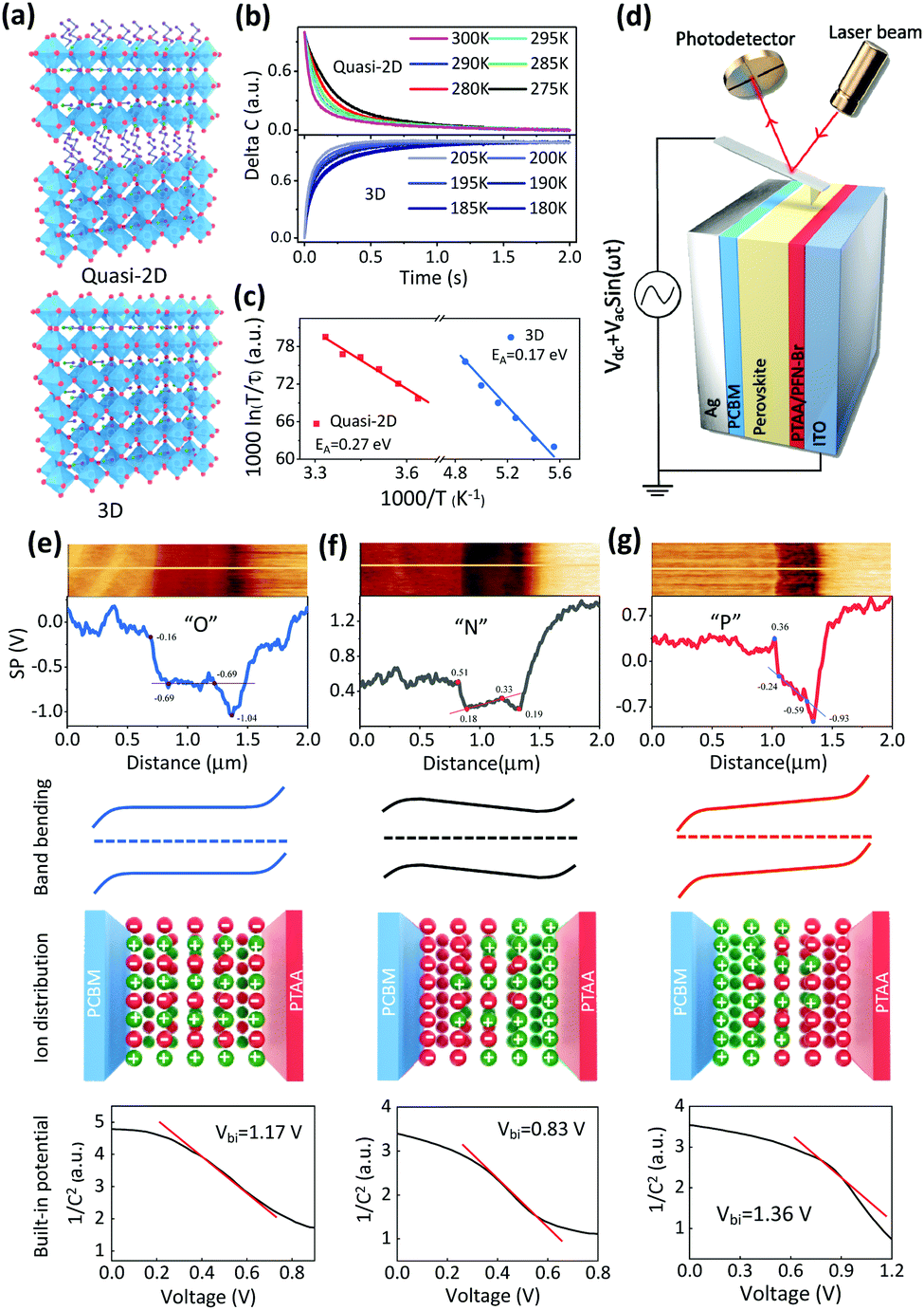 | ||
| Fig. 1 Ion migration and accumulation in quasi-2D and 3D PVSCs. (a) Crystal structures of the quasi-2D BA2MAn−1PbnI3n+1 perovskite and 3D MAPbI3 perovskite. (b and c) Results of TID measurements for quasi-2D PVSC and 3D PVSCs: (b) capacitance transients from anion migration (drift), and (c) Arrhenius fitting results of anion migration. (d) Schematic illustration of SKPM measurements. (e–g) From top to bottom: surface potential image by SKPM mapping, line-cutting profile of surface potential distribution (along the white line in the SKPM mapping images), schematic diagram of band bending derived from the surface potential profile, schematic diagram of the ion distribution profile, and Mott–Schottky characterization, i.e., (1/C2)–V plot for the quasi-2D GA0.2BA1.8MA5Pb6I19 PVSC with (e) “O” (no ion accumulation), (f) “N” (unfavorable ion accumulation) and (g) “P” (favorable ion accumulation). | ||
Results and discussion
Ion migration
First, the ion migration behavior of the quasi-2D GA0.2BA1.8MA5Pb6I19 perovskite is studied and compared with that of the 3D MAPbI3 perovskite (Fig. 1a). Halide perovskites can be made with different dimensionalities.50,51 Basically, the 3D perovskite structure is a corner-sharing octahedral inorganic structure that extends in three dimensions. In particular, the …Pb–I–Pb–I… connection is not disrupted in any direction. In the 2D perovskites, the corner-sharing octahedra are connected in 2 dimensions, i.e., in a single plane, with the direction vertical to the 2D plane interrupted by large 2D spacer molecules that hold the structure together via van der Waals interactions. In a pure 2D perovskite, the octahedral plane consists of one layer of octahedra. Quasi-2D perovskites also have a 2D structure, but the 2D plane is composed of more than one layer of octahedra in the Z direction. Here we focus on quasi-2D perovskites, given their high lattice formation and ion migration activation energies. These features slow down the ion migration due to external stresses in the corresponding perovskite solar cells, enabling the study of ion-migration effects. Over the years, these materials and procedures for fabricating devices with them have been optimized by us.2,7,52–54 X-ray diffraction (XRD) patterns of 3D and quasi-2D PVSC are shown in Fig. S1 (ESI†). The 2θ peaks at 14.1° and 28.4° correspond to the (110) and (220) lattice planes, respectively, of the 3D MAPbI3 perovskite. The peaks at 14.1° and 28.4° correspond to the (111) and (202) lattice planes, respectively, of the quasi-2D GA0.2BA1.8MA5Pb6I19 perovskite.The transient ion-drift (TID) method,55,56 which is well-established to measure ion migration, as reported previously,55–58 is used to characterize ion migration within the perovskite films.57,58 The TID method enables us to derive from its results the basic ion-migration parameters, such as the ion diffusion coefficient and the activation energy. Moreover, the charge of the migrating ion species can be determined. More details about this characterization method can be found in the Experimental section in the ESI.†![[thin space (1/6-em)]](https://www.rsc.org/images/entities/char_2009.gif) 57Fig. 1b shows the temperature-dependent capacitance variation of quasi-2D and 3D PVSCs. Ion migration is a thermally activated process. Because an activation energy must be overcome, the response speed increases with increasing temperature, as measured in TID. The change in response is found to follow an Arrhenius relation. However, for MAPbI3, ion migration becomes experimentally measurable at 180 K, and a much higher temperature, up to 270 K, is required to activate ion migration for the quasi-2D GA0.2BA1.8MA5Pb6I19 perovskite. This finding agrees with the less mobile nature of ions in the quasi-2D perovskite compared with the 3D analog. Fig. 1c and Fig. S2 (ESI†) show Arrhenius fits, based on different ion-migration species, i.e., 0.17 eV and 0.25 eV, which, in our case, can be assigned to I− and MA+ of MAPbI3 (Table S1, ESI†), respectively, based on previous work.57,59 Interestingly, for the 2D GA0.2BA1.8MA5Pb6I19 PVSC (Fig. 1b and c, and Fig. S3 and Table S1, ESI†), only anion migration is detected, with a migration activation energy of 0.27 eV, which is slightly higher than that (0.25 eV) of its 3D analogue. This higher anion-migration activation energy is attributed to the higher formation energy of the quasi-2D than the 3D perovskites, which has been attributed to changes in van der Waals interactions between the [PbI6] units and the organic cations.60,61 As a result, I− migration in a 2D perovskite requires more energy than in 3D MAPbI3.37,60,62 It is also worth noting that, due to the considerable stability at room temperature for 2D PVSCs (Fig. S4, ESI†), even though the high temperature will increase ion migration, as extrapolated from TID results at higher temperatures, this will not affect the corresponding results.
57Fig. 1b shows the temperature-dependent capacitance variation of quasi-2D and 3D PVSCs. Ion migration is a thermally activated process. Because an activation energy must be overcome, the response speed increases with increasing temperature, as measured in TID. The change in response is found to follow an Arrhenius relation. However, for MAPbI3, ion migration becomes experimentally measurable at 180 K, and a much higher temperature, up to 270 K, is required to activate ion migration for the quasi-2D GA0.2BA1.8MA5Pb6I19 perovskite. This finding agrees with the less mobile nature of ions in the quasi-2D perovskite compared with the 3D analog. Fig. 1c and Fig. S2 (ESI†) show Arrhenius fits, based on different ion-migration species, i.e., 0.17 eV and 0.25 eV, which, in our case, can be assigned to I− and MA+ of MAPbI3 (Table S1, ESI†), respectively, based on previous work.57,59 Interestingly, for the 2D GA0.2BA1.8MA5Pb6I19 PVSC (Fig. 1b and c, and Fig. S3 and Table S1, ESI†), only anion migration is detected, with a migration activation energy of 0.27 eV, which is slightly higher than that (0.25 eV) of its 3D analogue. This higher anion-migration activation energy is attributed to the higher formation energy of the quasi-2D than the 3D perovskites, which has been attributed to changes in van der Waals interactions between the [PbI6] units and the organic cations.60,61 As a result, I− migration in a 2D perovskite requires more energy than in 3D MAPbI3.37,60,62 It is also worth noting that, due to the considerable stability at room temperature for 2D PVSCs (Fig. S4, ESI†), even though the high temperature will increase ion migration, as extrapolated from TID results at higher temperatures, this will not affect the corresponding results.
Ion accumulation
The profile of ion accumulation in a quasi-2D GA0.2BA1.8MA5Pb6I19 PVSC was studied. Within this perovskite the most probable migrating ion is I−, given that only anion migration is detected as shown in Fig. 1c. Regarding anion accumulation, it has not yet been possible to observe it directly (using an isotope tracer), but even minimal migration leading to ion accumulation at interfaces will induce a significant change in the electrostatic potential.21 The accumulation of mobilized ions tends to affect the space charge region, change the internal electric field, and, via a change in the electrostatic potential profile, affect the electron's electrochemical potential across the PVSCs. Conversely, changes in the electrochemical potential of the electrons are a reasonable way to follow the effects of ion accumulation in PVSCs. Therefore, scanning Kelvin probe microscopy (SKPM) (Fig. 1d) is selected to record the electrochemical potential differences of the electrons, and, in that way, to map ion accumulation in quasi-2D PVSCs via the device's vertical cross-section (Fig. 1e–g and Fig. S5, ESI†) under different external stresses.Without any stressing, the quasi-2D PVSCs exhibit strong band bending of +0.53 eV and +0.35 eV at the cathode (PC61BM/perovskite) and anode (PTAA/perovskite) interfaces, respectively (Fig. 1e). By contrast, the perovskite bulk region of the PVSC exhibits a constant electrochemical potential (or flat band). These results suggest that no ion accumulation occurs (abbreviated as “O”) in quasi-2D PVSCs without any post-treatment, which we ascribe to the low ion mobility in quasi-2D perovskites. After thermal stressing, ion migration occurs, and ion accumulation due to the Vbi becomes pronounced. As a result, the band bending of quasi-2D PVSCs at perovskite/cathode and PTAA/anode interfaces decreases significantly to +0.33 eV and +0.14 eV, respectively (Fig. 1f). Moreover, the electrochemical potential is no longer flat in the perovskite bulk region, but increases by −0.15 eV, thus reducing the effective Vbi by +0.56 eV. This observation is consistent with an increasing gradient of anions from anode to cathode interfaces, and/or vice versa for cations (Fig. 1f).
We then studied the effect of simultaneous heat (373 K) plus light co-activation (white light from a Xe lamp with an intensity of 0.12 mW cm−2) on the ion migration and accumulation behavior of quasi-2D PVSCs. As shown in Fig. 1g, the band bending changed to around +0.60 and +0.34 eV at the cathode and anode interfaces, respectively. Interestingly, the electron electrochemical potential in the bulk perovskite shows a gradient from the cathode to the anode of around +0.35 eV, which is of the same polarity as the Vbi. This indicates an increasing gradient of anions from cathode to anode interfaces, and vice versa for cations (Fig. 1g). As a result, the built-in potential of the quasi-2D PVSC after light activation is significantly increased by +0.41 eV. To the best of our knowledge, this is the first example of such favorable ion accumulation attained in PVSCs. Fig. 1e–g also show the Mott–Schottky analyses of capacitance–voltage measurements, and the fitting results are shown in Fig. S6 (ESI†). We find that the slope of the Mott–Schottky plots has a trend of “P” < “O” < “N” and the measured dopant concentrations have a trend of “N” < “O” < “P”. The built-in potentials for the PVSCs with “O”, “N”, “P” are 1.17 V, 0.83 V, 1.36 V, respectively. These results are consistent with the results from SKPM measurements, and agree with our interpretation of changes in the built-in potential due to different types of ion accumulation.
Device performance
Fig. 2a shows the J–V characteristic curves of the quasi-2D PVSCs with a planar heterojunction structure54 after the different treatments, and the corresponding device parameters are summarized in Table 1. The optimal quasi-2D PVSCs with “O” show a PCE of 14.61% with a VOC of 1.17 V, an FF of 0.76, and a JSC of 16.33 mA cm−2, which is consistent with previous reports.2,63 However, the best quasi-2D PVSCs with “N” yield a significantly poorer efficiency of 4.31%, a VOC of 1.02 V, an FF of 0.65, and a JSC of 6.50 mA cm−2. The drop in device performance with “N” is consistent with the literature reports.46,57 Encouragingly, with “P”, the optimal quasi-2D PVSCs exhibit a significantly improved PCE of up to 19.05%, a VOC of 1.25 V, an FF of 0.80, and a JSC of 19.06 mA cm−2. This represents one of the best results among quasi-2D PVSCs. After stopping the thermal–light co-treatment, the PCE shows almost no change over 7.5 days, indicating the good device stability (Fig. S7, ESI†). The significant variation in device performance with the different ion accumulation statuses is further confirmed by the statistic histogram of the efficiencies (average PCE values of 13.17 ± 0.85%, 3.58 ± 0.58% and 18.46 ± 0.31% for PVSCs with “O”, “N” and “P”, respectively), for more than 30 devices for each treatment (Fig. 2b). Notably, the efficiency distribution becomes much narrower after the post-treatments, especially after thermal–light co-activation. As a result, we conclude that ion accumulation can significantly affect the performance of PVSCs. The stability of the devices with “P”, operating at their MPP (maximum power point), is shown in Fig. S8 (ESI†). The PCE remained stable during the measurements, indicating good operational stability. Interestingly, for another 2D device, based on the (3AMP)(MA0.75FA0.25)3Pb4I13 perovskite (Fig. S9, ESI†), we find that the thermal–light co-treatment improved device performance and the PCE increases from 17.18% to 18.94%, indicating the potential of thermal–light co-treatment to be applied to other stable perovskites.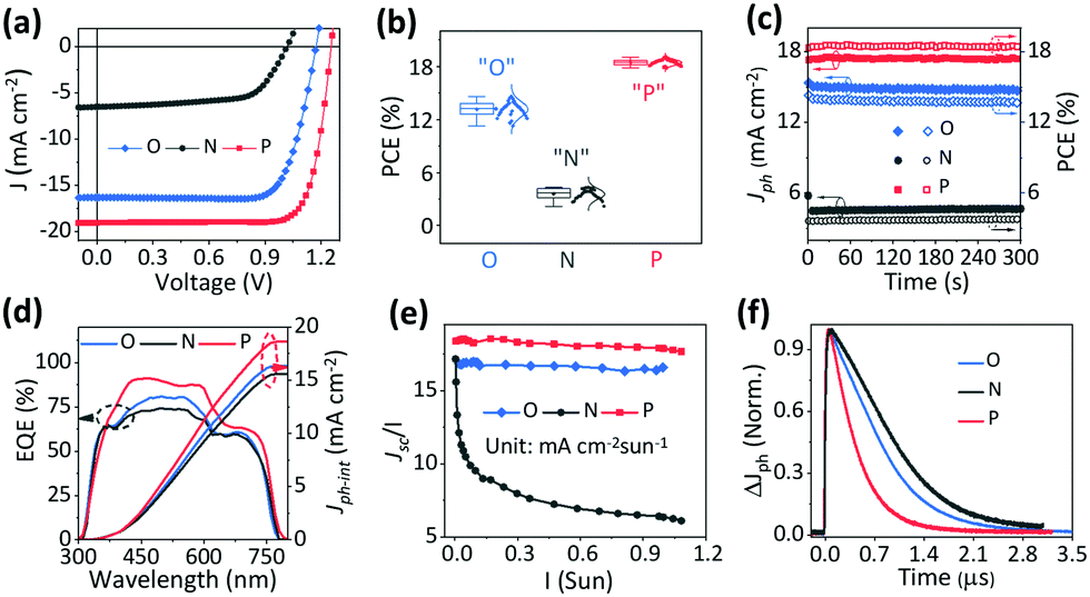 | ||
| Fig. 2 Device performance variation of quasi-2D PVSCs with different types of ion accumulation: “O” no treatment, no ion accumulation; “N” thermal treatment, unfavorable ion accumulation; and “P” thermal + light treatment, favorable ion accumulation. (a) J–V characteristic curves, (b) PCE histograms of 30 devices, (c) stabilized photocurrent measurements and PCE output at the maximum power point, (d) EQE spectra and integrated photocurrent curves, (e) carrier generation efficiency under different light intensities, and (f) TPC decay kinetics. | ||
| Ion accumulation | V OC (V) | J SC (mA cm−2) | FF | PCEmax/ave (%) | J ph-int (mA cm−2) |
|---|---|---|---|---|---|
| “O” | 1.17 | 16.33 | 0.76 | 14.61/13.17 ± 0.85 | 16.33 |
| “N” | 1.02 | 6.50 | 0.65 | 4.31/3.58 ± 0.58 | 15.58 |
| “P” | 1.25 | 19.06 | 0.80 | 19.05/18.46 ± 0.31 | 18.68 |
The quasi-2D PVSCs with “O”, “N” and “P” show steady-state output power efficiencies of 13.75%, 3.70%, and 18.43% (Fig. 2c and Table S2, ESI†), respectively, which is consistent with those from J–V measurements. Besides, negligible hysteresis is observed (Fig. S10 and Table S3, ESI†) in the quasi-2D PVSCs with “O” and “P”, which we ascribe to the low mobility of ions at room temperature. Moreover, the large hysteresis index (HI) for the quasi-2D device with “N”, possibly due to the poor charge extraction, makes the device performance more sensitive to ion accumulation. This behavior can be compared with that of a 3D perovskite-based PV device (Fig. S11 and Table S3, ESI†) that exhibits a much larger HI of 14.5% than the quasi-2D devices with “O” and “P”. With “O”, the quasi-2D PVSCs show a peak EQE of 80.86% at 500 nm, with a relatively weak response from 620 nm to 770 nm (Fig. 2d). With “N”, the EQE peak decreases to 73.85%, while the response from 620 nm to 770 nm is largely intact. For quasi-2D PVSCs with “P”, the EQE response dramatically increases over the entire absorbing region. The corresponding integrated photocurrents (Jph-int) are 16.33, 15.58, and 18.68 mA cm−2 for the quasi-2D PVSCs with “O”, “N”, and “P”, respectively. Since the quasi-2D PVSC exhibits the same optical absorption profile due to the same device structure, the above results indicate that the internal carrier dynamics can be greatly affected by the ion accumulation. The whole set of measurements completes the internal check on the device performance, and is consistent with ion accumulation being able to greatly affect the device performance, by changing the electrostatic potential profile and, via this, affecting the carrier dynamics.
Carrier dynamics
X-ray diffraction (XRD) patterns of the quasi-2D PVSCs with “O”, “N”, “P” are shown in Fig. S12 and Table S4 (ESI†); they show negligible differences. Therefore, any variation of the device performance is not due to any change in the perovskite crystal structure.2,60 Furthermore, we studied the light-intensity-dependent charge-extraction efficiency under short-circuit conditions. The charge collection efficiency can be assessed fairly by studying the JSC ∝ Iα at different I, where I is the light intensity. As shown (Fig. S13, ESI†), the α values are 0.99, 0.83, and 1.00 for quasi-2D PVSCs with “O”, “N”, and “P”, respectively. The α value of 0.83 for PVSCs with unfavorable ion accumulation fits with reduced charge extraction at high photo-carrier concentrations. The α values of the “O” and “P” are almost similar and are close to 1, and all the carriers are swept out before recombination at high photo-carrier concentrations. The plots of JSC/I against I in Fig. 2e, derived from Fig. S13 (ESI†), show the light-intensity-dependent carrier-generation difference between “P” and, to a slightly lesser extent also “N”, on the one hand, and “O”, on the other hand. This behavior confirms the photocarrier generation property variation for different types of ion accumulation. In “O”, JSC/I decreased rapidly with the increasing light intensity due to severe biomolecular recombination as shown in Fig. S13 (ESI†), and this accounts for the mismatch between Jph-int and JSC from the J–V curve.Furthermore, transient photocurrent (TPC) measurements were carried out to directly examine the effect of different types of ion accumulation behavior on the charge extraction. TPC measurements record the photocurrent decay under short-circuit conditions, where most of the photocarriers are expected to be swept out of the device, driven by the Vbi, and, consequentially, the transit time can be derived to assess the carrier extraction of the PVSCs. As shown in Fig. 2f, the quasi-2D PVSCs with “N”, “O”, and “P” exhibit a gradually reduced carrier transit time, demonstrating improved charge-collection properties. These can be attributed to the change in the driving force (Vbi) as a result of the different ion accumulation conditions, which strongly affect the carrier generation and charge extraction and, thus, JSC and FF values.64,65
Electrical poling
The most direct way to construct ion migration/accumulation is via electrical poling, which adds an external electrical potential difference to Vbi. With different magnitudes and polarities of the applied poling voltages, i.e., −1.12 V, 0.0 V, 0.7 V, 1.12 V, and 2.0 V, the quasi-2D PVSCs are electrically poled during thermal activation to construct different ion-accumulation profiles in the perovskite, to look for correlations with the device performance (Fig. S14, ESI†). Considering the Vbi of PVSCs, the ion accumulation in the PVSCs should be determined by the net internal voltage (Vint = Vpoling − Vbi) within the quasi-2D PVSCs. With the electrical poling voltage increasing from −1.12 V to 2.0 V, Vint gradually increases from −2.3 to 0.8 V, and the corresponding ion accumulation is expected to gradually turn from “N” to “P”. The device performance variation after different electrical poling conditions also exhibits large differences, as shown in Fig. S15 (ESI†); a summary is given in Fig. 3a and Table S5 (ESI†).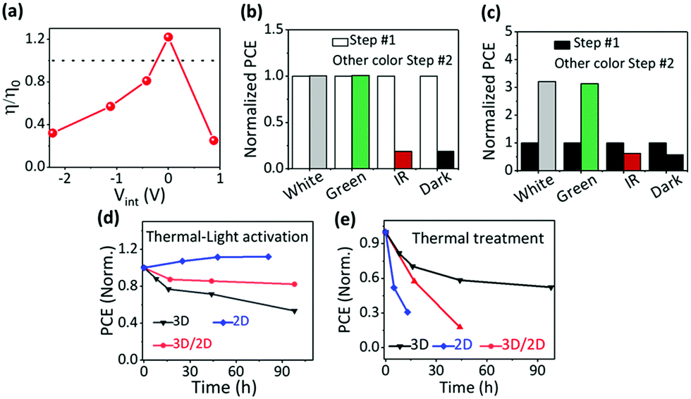 | ||
| Fig. 3 Device light-to-electrical power efficiency variation of quasi-2D PVSCs under different external stresses: (a) as a function of the thermal–electrical poling voltage (dotted line: η/η0 = 1, the control PCE); (b) for different thermal–light co-treatments during the second phase (Step #2) after thermal–light co-treatment (Step #1); and (c) for different thermal–light co-treatments during the second phase (Step #2) after thermal treatment in the dark (Step #1). Efficiency variation of 3D MAPbI3, quasi-2D and 3D/2D heterojunction PVSCs with different post-treatments: (d) thermal–light activation, and (e) thermal treatment in the dark. | ||
With the Vint gradually increasing from −2.3 to 0 V, the change in the device performance gradually changes from negative (worse) to positive (better). The straightforward correlation between Vint and the device performance variation presents strong support for the effect, on device performance, of ion accumulation in the perovskite. The performance, compared with the as-prepared device, increases by 22% with Vint ≈ 0 V (i.e., Vpoling = Vbi), and the improved device performance (best efficiency 13.46%) is much lower than that obtained with thermal–light activation (Fig. 2b); this performance is, however, well within the range of “O” devices, suggesting that we do not get to a “P” state. A drop in the device performance is observed with a Vint of 0.8 V, possibly due to electrochemical reactions at the electrode interfaces, which induced permanent degradation.26,27 These results confirm that ion accumulation indeed affects the device performance.
Effect of photon energy
Considering that white light involves photons of different energies, we study the effect of the incident photon energy (or the activation light wavelength) on the device performance of quasi-2D PVSCs in the “P” state. Since adding light to thermal activation gave a more reproducible device performance with a narrower PCE distribution (Fig. 2b), we performed post-treatments (white light) on the quasi-2D PVSCs first (Step #1) in order to precisely evaluate the effects of the subsequent thermal–light co-treatments (Step #2), i.e., 525 ± 5 nm (green light), 895 ± 45 nm (IR), white light, and dark conditions. The quasi-2D PVSCs with green-light or white-light illumination show almost no change in PCE after the Step #2 treatment (Fig. 3b and Fig. S16, Table S6, ESI†). With IR illumination the PCE decreased rapidly, similar to the case with thermal annealing in the dark. In the parallel group with thermal annealing in the dark as the first treatment step, and with subsequent different thermal–light co-treatments (second step), the quasi-2D PVSCs exhibit a significant increase in PCE after green- or white-light activation (Fig. 3c and Fig. S17, Table S7, ESI†), although the device performance becomes worse after IR stressing, and is similar to that in the dark (“O”). These results imply that the device performance is switchable with different post-treatments. Based on the results from the TID and SKPM experiments (Fig. 1) we ascribe these differences to the different effects of ion migration. Considering that the absorption edge of the quasi-2D PVSCs is around 770 nm (Fig. S18, ESI†), we conclude that supra-band-gap light activation is key to generating the “P” state. In addition, the increase in the quasi-2D PVSC device conversion efficiency upon light activation after thermal degradation indicates that light-activation-induced ion accumulation can potentially enable the long-term stability of PVSCs. As shown in Fig. S19 and Table S8 (ESI†), after storage in the dark at 85 °C for 105 h, the PCE decreased rapidly from 16.73% to 1.60%. After subsequent thermal–light activation (100 °C) for 25 h, the PCE returned to 16.22%, close to its original value.Effect of ion migration
Different perovskite structures exhibit different types of ion migration behavior (Fig. 1), and the effects of the perovskite type on the ion accumulation and the device performance after the same post-treatments mentioned above were studied to unravel the effect of ion migration on the ion accumulation and subsequent device performance. The external stressing conditions, i.e., none, thermal and thermal–light co-activation, seem to have little effect on the electric potential profile of MAPbI3 PVSCs (Fig. S20, ESI†). This observation can be satisfactorily explained by facile ion migration of MAPbI3 at room temperature, which will allow ions to re-arrange to minimize the effects of ion accumulation. As a result, the device performance of PVSCs with thermal or thermal–light co-activation does not show much difference (Fig. 3d and e, and Fig. S21 and Table S9, ESI†), and the decrease in device efficiency compared with that without any treatment can be attributed to the thermally induced decomposition of the perovskite films and/or their interfaces with the contacting films.66–68Keeping in mind the large difference between ion migration of 3D MAPbI3 and the quasi-2D perovskite film, here we also studied the effect of 3D and 2D composite films with a planar tandem structure (or the so called 3D/2D heterojunction) on the device performance of PVSCs with different post-treatments. In the 3D/2D perovskite, ion migration at the cathode interface is less facile than in the bulk (MAPI3), which can be attributed to the 2D component; upon thermal treatment in the dark, the interface at the cathode (PCBM) is expected to drive the PVSC made with the 3D/2D into the “N” state, which switches to “P” with thermal–light activation, while the ion accumulation in the 3D MAPbI3 part, adjacent to the interface with the anode (PTAA), remains unaffected, as verified in Fig. S20 (ESI†). As shown in Fig. 3d and e and Fig. S22 (ESI†), the 3D/2D heterojunction PVSCs show only a very slight efficiency decrease with thermal–light co-activation, but a more severe one with thermal treatment in the dark. Because ion migration in the 2D perovskites is less facile than in 3D perovskites, the ion accumulation status driven under the different external stresses can be retained for a long time for 2D or quasi-2D perovskite layers, while it will relax within seconds or less for 3D perovskite layers (because of the lack of kinetic stabilization). Thus, even though after thermal-treatment unfavorable ion accumulation (“N”) forms, this will quickly relax to the original state for the 3D perovskite layer, and thus will have little effect on the J–V measurements for the device. For the quasi-2D perovskite layer, the “N” state can be retained, due to the slower kinetics, and this will ruin the device performance. Similar results can be expected and are observed for the thermal–light co-treatment (forming “P”). As a result, compared with the quasi-2D devices, the 3D devices show the best performance after heat treatment, but the worst after thermal–light co-treatment, while the quasi-2D or the 2D/3D structure will retain the favorable ion accumulation feature. Interestingly, the extent of 3D/2D PVSC efficiency variation lies between those of 3D and quasi-2D PVSCs. Therefore, we conclude that perovskite composition or the ion migration behavior indeed affect the ion accumulation and device performance of PVSCs, and ion accumulation in every part of the PVSCs, i.e., the halide perovskite bulk and its interfaces with the cathode and anode, affects the device performance.
Mechanism
By increasing the temperature of the perovskite, in the dark, ion migration in the quasi-2D perovskite is activated. The band bending structures in the dark and under illumination are shown in Fig. 4a, and have been well studied and established. The band bending structure will affect the ion migration and accumulation via the electrostatic potential profile, due to the formation of a space-charge region and charge diffusion. The anion (I−) tends to migrate toward the cathode (to the left in Fig. 4a), which is Ag in our case, due to Vbi as illustrated in Fig. 4a, and ion accumulation occurs. As a result, the “N” state forms according to Le Chatelier's principle. The accumulation of I− at the perovskite/PCBM interface might cause a chemical reaction between I− and Ag to form AgI, which will cause irreversible device degradation. Notably, the “N” state that forms under thermal treatment will be “frozen” at room temperature, thus forming a relatively stable ion-accumulation status (on the time scales of our experiments) due to the low ion migration of quasi-2D PVSCs. As a result, the effect of post-treatment on the ion accumulation status becomes valid only in perovskites with low ion-migrating properties, as confirmed above (Fig. 1, Fig. 3d and e, and Fig. S22, ESI†).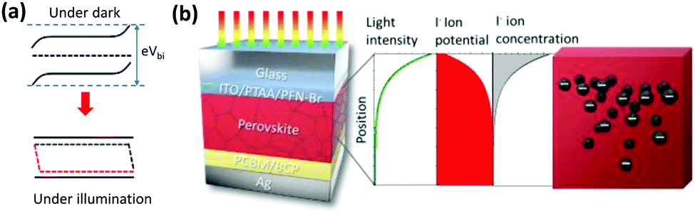 | ||
| Fig. 4 Proposed mechanism underlying different types of ion accumulation formed using different post-treatments. (a) Schematic diagrams of the band bending of quasi-2D PVSCs in the dark and when illuminated. (b) Schematic diagram of the device structure (left) and the light-intensity distribution, ion-potential distribution, and ion-concentration distribution (as plots and as a cartoon) in quasi-2D PVSCs (right). | ||
We can propose a possible mechanism for the formation of the “P” state in quasi-2D PVSCs with thermal and light co-treatment. On the one hand, upon light absorption with supra-band-gap photons, photo-carriers are generated, which results in quasi-Fermi level splitting due to the existence of unbalanced charge-carrier densities (Fig. 4a). Under open-circuit conditions, the quasi-Fermi level splitting screens the Vbi, and results in a quasi-flat-band structure (Fig. 4a).69 As a result, the ion migration or accumulation driven by Vbi or formation of the “N” state can be avoided, and this constitutes an important step to transition from “N” to “P” with light activation. On the other hand, the light-intensity distribution in PVSCs is not even, but decays exponentially, according to the Lambert–Beer law (Fig. 4b). The uneven light-intensity distribution induces an ion potential difference,70–72 which serves as another driving force to form the “P” state. In this case, I− tends to migrate toward the anode, which is the ITO, and less I− accumulates near the Ag cathode, mitigating the chemical reaction and suppressing the degradation. A similar phenomenon has also been reported in previous work,73 where a light-induced I− concentration re-distribution was observed in a MAPbI3 perovskite film.
Conclusions
In summary, by using different external stressing conditions, i.e., thermal, light, a bias or combinations of these, we are able to tailor the ion accumulation in PVSCs to arrive at a “favorable” ion accumulation, where an electric field is generated with the same polarity as the built-in potential of PVSCs. Such ion accumulation significantly improves the device performance from 14.61% to 19.05%, which we ascribe to an improvement in the carrier dynamics, and is one of the best efficiency results for quasi-2D PVSCs. The results of further studies on the effects of electrical poling, the wavelength of the exciting light and extension to more perovskite systems are in agreement with the ion-accumulation effects on the device performance. The different types of ion accumulation that explain our results fit well with ion migration under a built-in potential, quasi-Fermi level splitting and potential differences that are due to the gradient in the absorbed light intensity in the perovskite, as well as in the direction between the contacts.Author contributions
X. Lian, L. Zuo, B. Chen, and B. Li contributed equally to this work. H. Chen, L. Zuo and D. Cahen supervised the project. X. Lian carried out the experiments and performed PVSC fabrication and characterization. H. Wu performed J–V measurements for 2D PVSCs supervised by G. Wu. S. Shan performed 3D PVSC fabrication. B. Li, X. Yu, and D. Yang carried out TID measurements and analysis. B. Chen, Q. Chen and L. Chen conducted SKPM measurements and analyzed the data. X. Lian, L. Zuo, H. Chen, and D. Cahen wrote the paper. All authors discussed results, read, and commented on the manuscript.Conflicts of interest
There are no conflicts to declare.Acknowledgements
H. Chen and D. Cahen acknowledge support of a joint National Natural Science Foundation of China, NSFC − Israel Science Foundation, ISF, program, grants NSFC 51961145301 and ISF 3098/19. We further thank NSFC for support via grants (51620105006, 52173185, 62025403, 51973184 and 61721005, 22022205). We also acknowledge gratefully the “Pioneering” and “Leading Goose” R&D Program of Zhejiang (2022C01104), research start-up fund from Zhejiang University, Qizhen Research Fund from Zhejiang University (K20220132), technical support on SKPM measurements from Nano-X, SINANO and the National Key Research and Development Program of China (no. 2019YFA0705900).Notes and references
- J. Chen, L. Zuo, Y. Zhang, X. Lian, W. Fu, J. Yan, J. Li, G. Wu, C. Li and H. Chen, Adv. Energy Mater., 2018, 8, 1800438 CrossRef.
- X. Lian, J. Chen, M. Qin, Y. Zhang, S. Tian, X. Lu, G. Wu and H. Chen, Angew. Chem., Int. Ed., 2019, 58, 9409–9413 CrossRef CAS PubMed.
- C. S. Ponseca, Jr., T. J. Savenije, M. Abdellah, K. Zheng, A. Yartsev, T. Pascher, T. Harlang, P. Chabera, T. Pullerits, A. Stepanov, J. P. Wolf and V. Sundstrom, J. Am. Chem. Soc., 2014, 136, 5189–5192 CrossRef PubMed.
- L. Zuo, Z. Gu, T. Ye, W. Fu, G. Wu, H. Li and H. Chen, J. Am. Chem. Soc., 2015, 137, 2674–2679 CrossRef CAS PubMed.
- G. E.-E. Samuel, D. Stranks, G. Grancini, C. Menelaou, M. J.-P. Alcocer, T. Leijtens, L. M. Herz, A. Petrozza and H. J. Snaith, Science, 2013, 342, 341–344 CrossRef PubMed.
- G. Xing, N. Mathews, S. Sun, S. S. Lim, Y. M. Lam, M. Gratzel, S. Mhaisalkar and T. C. Sum, Science, 2013, 342, 344–347 CrossRef CAS PubMed.
- X. Zhang, G. Wu, W. Fu, M. Qin, W. Yang, J. Yan, Z. Zhang, X. Lu and H. Chen, Adv. Energy Mater., 2018, 8, 1702498 CrossRef.
- Y. Zhang, J. Chen, X. Lian, M. Qin, J. Li, T. R. Andersen, X. Lu, G. Wu, H. Li and H. Chen, Small Methods, 2019, 3, 1900375 CrossRef CAS.
- NREL, https://www.nrel.gov/pv/cell-efficiency.html.
- P. K. Nayak, S. Mahesh, H. J. Snaith and D. Cahen, Nat. Rev. Mater., 2019, 4, 269–285 CrossRef CAS.
- Y. Deng, E. Peng, Y. Shao, Z. Xiao, Q. Dong and J. Huang, Energy Environ. Sci., 2015, 8, 1544–1550 RSC.
- Y. Hu, Y. Chu, Q. Wang, Z. Zhang, Y. Ming, A. Mei, Y. Rong and H. Han, Joule, 2019, 3, 2076–2085 CrossRef CAS.
- D. R. Ceratti, A. Zohar, R. Kozlov, H. Dong, G. Uraltsev, O. Girshevitz, I. Pinkas, L. Avram, G. Hodes and D. Cahen, Adv. Mater., 2020, 32, 2002467 CrossRef CAS PubMed.
- E. Mosconi and F. De Angelis, ACS Energy Lett., 2016, 1, 182–188 CrossRef CAS.
- H. Zhang, X. Fu, Y. Tang, H. Wang, C. Zhang, W. W. Yu, X. Wang, Y. Zhang and M. Xiao, Nat. Commun., 2019, 10, 1088 CrossRef CAS PubMed.
- H. J. Snaith, A. Abate, J. M. Ball, G. E. Eperon, T. Leijtens, N. K. Noel, S. D. Stranks, T. W. Wang, K. Wojciechowski and W. Zhang, J. Phys. Chem. Lett., 2014, 5, 1511–1515 CrossRef CAS PubMed.
- W. Tress, N. Marinova, T. Moehl, S. M. Zakeeruddin, M. K. Nazeeruddin and M. Grätzel, Energy Environ. Sci., 2015, 8, 995–1004 RSC.
- J. Yan, W. Qiu, G. Wu, P. Heremans and H. Chen, J. Mater. Chem. A, 2018, 6, 11063–11077 RSC.
- A. R. Bowring, L. Bertoluzzi, B. C. O'Regan and M. D. McGehee, Adv. Energy Mater., 2018, 8, 1702365 CrossRef.
- C.-H. Li, M.-Y. Liao, C.-H. Chen and C.-C. Chueh, J. Mater. Chem. A, 2020, 8, 4294–4302 CAS.
- Y. B. Yuan, Q. Wang, Y. C. Shao, H. D. Lu, T. Li, A. Gruverman and J. S. Huang, Adv. Energy Mater., 2016, 6, 1501803 CrossRef.
- M. Stolterfoht, C. M. Wolff, J. A. Márquez, S. Zhang, C. J. Hages, D. Rothhardt, S. Albrecht, P. L. Burn, P. Meredith, T. Unold and D. Neher, Nat. Energy, 2018, 3, 847–854 CrossRef CAS.
- S. Meloni, T. Moehl, W. Tress, M. Franckevicius, M. Saliba, Y. H. Lee, P. Gao, M. K. Nazeeruddin, S. M. Zakeeruddin, U. Rothlisberger and M. Graetzel, Nat. Commun., 2016, 7, 10334–10342 CrossRef CAS PubMed.
- A. Pockett, G. E. Eperon, N. Sakai, H. J. Snaith, L. M. Peter and P. J. Cameron, Phys. Chem. Chem. Phys., 2017, 19, 5959–5970 RSC.
- D. Y. Son, S. G. Kim, J. Y. Seo, S. H. Lee, H. Shin, D. Lee and N. G. Park, J. Am. Chem. Soc., 2018, 140, 1358–1364 CrossRef CAS PubMed.
- C. Besleaga, L. E. Abramiuc, V. Stancu, A. G. Tomulescu, M. Sima, L. Trinca, N. Plugaru, L. Pintilie, G. A. Nemnes, M. Iliescu, H. G. Svavarsson, A. Manolescu and I. Pintilie, J. Phys. Chem. Lett., 2016, 7, 5168–5175 CrossRef CAS PubMed.
- A. Guerrero, J. You, C. Aranda, Y. S. Kang, G. Garcia-Belmonte, H. Zhou, J. Bisquert and Y. Yang, ACS Nano, 2016, 10, 218–224 CrossRef CAS PubMed.
- J. M. Azpiroz, E. Mosconi, J. Bisquert and F. De Angelis, Energy Environ. Sci., 2015, 8, 2118–2127 RSC.
- B. Chen, P. N. Rudd, S. Yang, Y. Yuan and J. Huang, Chem. Soc. Rev., 2019, 48, 3842–3867 RSC.
- R. A. Belisle, K. A. Bush, L. Bertoluzzi, A. Gold-Parker, M. F. Toney and M. D. McGehee, ACS Energy Lett., 2018, 3, 2694–2700 CrossRef CAS.
- D. W. Ferdani, S. R. Pering, D. Ghosh, P. Kubiak, A. B. Walker, S. E. Lewis, A. L. Johnson, P. J. Baker, M. S. Islam and P. J. Cameron, Energy Environ. Sci., 2019, 12, 2264–2272 RSC.
- Y. Hu, E. M. Hutter, P. Rieder, I. Grill, J. Hanisch, M. F. Aygüler, A. G. Hufnagel, M. Handloser, T. Bein, A. Hartschuh, K. Tvingstedt, V. Dyakonov, A. Baumann, T. J. Savenije, M. L. Petrus and P. Docampo, Adv. Energy Mater., 2018, 8, 1703057 CrossRef.
- J. P. Correa-Baena, et al. , Science, 2019, 363, 627 CrossRef CAS PubMed.
- M. Abdi-Jalebi, Z. Andaji-Garmaroudi, S. Cacovich, C. Stavrakas, B. Philippe, J. M. Richter, M. Alsari, E. P. Booker, E. M. Hutter, A. J. Pearson, S. Lilliu, T. J. Savenije, H. Rensmo, G. Divitini, C. Ducati, R. H. Friend and S. D. Stranks, Nature, 2018, 555, 497–501 CrossRef CAS PubMed.
- S. G. Motti, D. Meggiolaro, A. J. Barker, E. Mosconi, C. A.-R. Perini, J. M. Ball, M. Gandini, M. Kim, F. De Angelis and A. Petrozza, Nat. Photonics, 2019, 13, 532–539 CrossRef CAS.
- X. Zheng, Y. Hou, C. Bao, J. Yin, F. Yuan, Z. Huang, K. Song, J. Liu, J. Troughton, N. Gasparini, C. Zhou, Y. Lin, D.-J. Xue, B. Chen, A. K. Johnston, N. Wei, M. N. Hedhili, M. Wei, A. Y. Alsalloum, P. Maity, B. Turedi, C. Yang, D. Baran, T. D. Anthopoulos, Y. Han, Z.-H. Lu, O. F. Mohammed, F. Gao, E. H. Sargent and O. M. Bakr, Nat. Energy, 2020, 5, 131–140 CrossRef CAS.
- Y. Lin, Y. Bai, Y. Fang, Q. Wang, Y. Deng and J. Huang, ACS Energy Lett., 2017, 2, 1571–1572 CrossRef CAS.
- Z. R. Huang, A. H. Proppe, H. R. Tan, M. I. Saidaminov, F. R. Tan, A. Y. Mei, C. S. Tan, M. Y. Wei, Y. Hou, H. W. Han, S. O. Keley and E. H. Sargenet, ACS Energy Lett., 2019, 4, 1521–1527 CrossRef CAS.
- H. Lai, D. Lu, Z. Xu, N. Zheng, Z. Xie and Y. Liu, Adv. Mater., 2020, 32, 2001470 CrossRef CAS PubMed.
- Z. Xu, D. Lu, X. Dong, M. Chen, Q. Fu and Y. Liu, Adv. Mater., 2021, 33, 2105083 CrossRef CAS PubMed.
- H. Ren, S. Yu, L. Chao, Y. Xia, Y. Sun, S. Zuo, F. Li, T. Niu, Y. Yang, H. Ju, B. Li, H. Du, X. Gao, J. Zhang, J. Wang, L. Zhang, Y. Chen and W. Huang, Nat. Photonics, 2020, 14, 154–163 CrossRef CAS.
- X. Lian, H. Wu, L. Zuo, G. Zhou, X. Wen, Y. Zhang, G. Wu, Z. Xie, H. Zhu and H. Chen, Adv. Funct. Mater., 2020, 30, 2004188 CrossRef CAS.
- H. Wu, X. Lian, J. Li, Y. Zhang, G. Zhou, X. Wen, Z. Xie, H. Zhu, G. Wu and H. Chen, J. Mater. Chem. A, 2021, 9, 12566–12573 RSC.
- G. Xing, B. Wu, S. Chen, J. Chua, N. Yantara, S. Mhaisalkar, N. Mathews and T. C. Sum, Small, 2015, 11, 3606–3613 CrossRef CAS PubMed.
- T. Y. Yang, G. Gregori, N. Pellet, M. Gratzel and J. Maier, Angew. Chem., Int. Ed., 2015, 54, 7905–7910 CrossRef CAS PubMed.
- W. Nie, J. C. Blancon, A. J. Neukirch, K. Appavoo, H. Tsai, M. Chhowalla, M. A. Alam, M. Y. Sfeir, C. Katan, J. Even, S. Tretiak, J. J. Crochet, G. Gupta and A. D. Mohite, Nat. Commun., 2016, 7, 11574–11582 CrossRef CAS PubMed.
- Z. Xiao, Y. Yuan, Y. Shao, Q. Wang, Q. Dong, C. Bi, P. Sharma, A. Gruverman and J. Huang, Nat. Mater., 2015, 14, 193–198 CrossRef CAS PubMed.
- N.-G. Park, Nat. Mater., 2015, 14, 140–141 CrossRef CAS PubMed.
- T. L. Yongbo Yuan, Q. Wang, J. Xing, A. Gruverman and J. Huang, Sci. Adv., 2017, 3, 1602164 CrossRef PubMed.
- D. H. Cao, C. C. Stoumpos, O. K. Farha, J. T. Hupp and M. G. Kanatzidis, J. Am. Chem. Soc., 2015, 137, 7843–7850 CrossRef CAS PubMed.
- F. Zhang, H. Lu, J. Tong, J. J. Berry, M. C. Beard and K. Zhu, Energy Environ. Sci., 2020, 13, 1154–1186 RSC.
- X. Lian, J. Chen, Y. Zhang, M. Qin, T. R. Andersen, J. Ling, G. Wu, X. Lu, D. Yang and H. Chen, J. Mater. Chem. A, 2019, 7, 19423–19429 RSC.
- X. Lian, J. Chen, Y. Zhang, S. Tian, M. Qin, J. Li, T. R. Andersen, G. Wu, X. Lu and H. Chen, J. Mater. Chem. A, 2019, 7, 18980–18986 RSC.
- Z. S. Yang, L. G. Yang, G. Wu, M. Wang and H. Z. Chen, Acta Chim. Sin., 2011, 69, 627–632 CAS.
- A. M.-T. Heiser, Appl. Phys. A: Solids Surf., 1993, 57, 325–328 CrossRef.
- A. Zamouche, T. Heiser and A. Mesli, Appl. Phys. Lett., 1995, 66, 631–633 CrossRef CAS.
- M. H. Futscher, J. M. Lee, L. McGovern, L. A. Muscarella, T. Wang, M. I. Haider, A. Fakharuddin, L. Schmidt-Mende and B. Ehrler, Mater. Horizons, 2019, 6, 1497–1503 RSC.
- M. H. Futscher, M. K. Gangishetty, D. N. Congreve and B. Ehrler, J. Chem. Phys., 2020, 152, 0442021 CrossRef PubMed.
- B. Li, C. Kan, P. Hang, Y. Fang, L. Zuo, L. Song, Y. Zhang, D. Yang and X. Yu, Phys. Status Solidi RRL, 2021, 15, 2100225 CrossRef CAS.
- X. Zhang, X. D. Ren, B. Liu, R. Munir, X. J. Zhu, D. Yang, J. B. Li, Y. C. Liu, D. M. Smilgies, R. P. Li, Z. Yang, T. Q. Niu, X. L. Wang, A. Amassian, K. Zhao and S. Z.-F. Liu, Energy Environ. Sci., 2017, 10, 2095–2102 RSC.
- L. N. Quan, M. Yuan, R. Comin, O. Voznyy, E. M. Beauregard, S. Hoogland, A. Buin, A. R. Kirmani, K. Zhao, A. Amassian, D. H. Kim and E. H. Sargent, J. Am. Chem. Soc., 2016, 138, 2649–2655 CrossRef CAS PubMed.
- J. Cho, J. T. DuBose, A. N.-T. Le and P. V. Kamat, ACS Mater. Lett., 2020, 2, 565–570 CrossRef CAS.
- M. Long, T. Zhang, D. Chen, M. Qin, Z. Chen, L. Gong, X. Lu, F. Xie, W. Xie, J. Chen and J. Xu, ACS Energy Lett., 2019, 4, 1025–1033 CrossRef CAS.
- M. Stolterfoht, C. M. Wolff, Y. Amir, A. Paulke, L. Perdigón-Toro, P. Caprioglio and D. Neher, Energy Environ. Sci., 2017, 10, 1530–1539 RSC.
- B. Qi and J. Wang, Phys. Chem. Chem. Phys., 2013, 15, 8972–8982 RSC.
- W. Chen, H. Chen, G. Xu, R. Xue, S. Wang, Y. Li and Y. Li, Joule, 2019, 3, 191–204 CrossRef CAS.
- W. Ligang, Z. Huanping, H. Junnan, H. Bolong, S. Mingzi, D. Bowei, Z. Guanghaojie, H. Yuan, C. Yihua, L. Liang, X. Ziqi, L. Nengxu, L. Zheng, C. Qi, S. Ling-Dong and Y. Chun-Hua, Science, 2019, 363, 265–270 CrossRef PubMed.
- K. Domanski, E. A. Alharbi, A. Hagfeldt, M. Grätzel and W. Tress, Nat. Energy, 2018, 3, 61–67 CrossRef CAS.
- P. Caprioglio, M. Stolterfoht, C. M. Wolff, T. Unold, B. Rech, S. Albrecht and D. Neher, Adv. Energy Mater., 2019, 9, 1901631 CrossRef.
- J. F. Guillemoles and D. Cahen, Ionics, 1996, 2, 143–154 CrossRef CAS.
- F. Varsano, D. Cahen, F. Decker, J. F. Guillemoles and E. Masetti, J. Electrochem. Soc., 1998, 145, 4212–4218 CrossRef CAS.
- F. Varsano, E. Masetti, J. F. Guillemoles, F. Decker and D. Cahen, Ionics, 1997, 3, 420–426 CrossRef CAS.
- D. W. deQuilettes, W. Zhang, V. M. Burlakov, D. J. Graham, T. Leijtens, A. Osherov, V. Bulovic, H. J. Snaith, D. S. Ginger and S. D. Stranks, Nat. Commun., 2016, 7, 11683–11691 CrossRef CAS PubMed.
Footnotes |
| † Electronic supplementary information (ESI) available. See DOI: https://doi.org/10.1039/d2ee01097f |
| ‡ These authors contributed equally to this work. |
| This journal is © The Royal Society of Chemistry 2022 |