
 Open Access Article
 This Open Access Article is licensed under a Creative Commons Attribution-Non Commercial 3.0 Unported Licence
The role of high-energy phonons in electron–phonon interaction at conducting surfaces with helium-atom scattering
G.
Benedek
 ab,
J. R.
Manson
ac and
Salvador
Miret-Artés
*ad
ab,
J. R.
Manson
ac and
Salvador
Miret-Artés
*ad
aDonostia International Physics Center (DIPC), Paseo Manuel de Lardizabal, 4, 20018 Donostia-San Sebastian, Spain
bDipartimento di Scienza dei Materiali, Università di Milano-Bicocca, Via Cozzi 55, 20125 Milano, Italy
cDepartment of Physics and Astronomy, Clemson University, Clemson, South Carolina 29634, USA
dInstituto de Física Fundamental, Consejo Superior de Investigaciones Científicas, Serrano 123, 28006 Madrid, Spain. E-mail: s.miret@iff.csic.es
First published on 13th September 2022
Abstract
In previous works it has been shown that the Debye–Waller (DW) exponent for Helium atom specular reflection from a conducting surface, when measured as a function of temperature in the linear high-temperature regime, allows for the determination of the surface electron–phonon coupling. However, there exist a number of experimental measurements that exhibit non-linearities in the DW exponent as a function of the surface temperature. Such non-linearities have been suggested as due to vibrational anharmonicity or a temperature dependence of the surface carrier concentration. In this work, it is suggested, on the basis of a few recent experimental data, that the deviations from linearity of the DW exponent temperature-dependence, as observed for conducting surfaces or supported metal overlayers with the present high-resolution He-atom scattering, permit to single out the specific role of high-energy phonons in the surface electron–phonon mass-enhancement factor.
1 Introduction
In 1929 Otto Stern with his helium-atom scattering (HAS) experiments from a crystal surface filled two needs with one deed: proving the quantum particle-wave duality for atoms and the ordered structure of crystal surfaces. The development of supersonic monochromatic (ΔE < 0.5 meV) He-beam spectrometers paved the way to high-resolution momentum-resolved spectroscopy of surface dynamics on the atomic scale. More needs fulfilled and envisaged by Stern! Unlike thermal neutrons and X-rays, thermal neutral He atoms probe the surface ∼0.3 nm away from the first atomic plane, and exchange energy and momentum with the solid atoms only via the interposed electrons. Thus, phonons are detected via the electron–phonon (e–ph) interaction, and not just at the surface, but possibly as deep below the surface as the range of that interaction. This sort of quantum sonar allows for the direct measurement of the e–ph coupling strength for each individual phonon (mode-λ spectroscopy),1 and for ultimately answering the question about phonon-mediated pairing in (2D-) superconductors: whos doing the job? The venerable concept of Debye–Waller (DW) factor, by which Piet Debye (1913) and Ivar Waller (in his 1923 thesis) correctly attributed to thermal vibrations the attenuation of Roentgen rays, in the case of HAS from conducting surfaces presently allows for a direct measurement of the e–ph mass-enhancement factor λ – a basic parameter for conducting materials.2 This is made possible by the theoretical demonstration that the linear decay of the DW exponent 2W(T) with the surface temperature T is approximately proportional to λ, with the proportionality constant estimated from known parameters of the surface.In the last decade, measurements of the HAS-DW factor 2W(T) = ln[I00(T)/I00(0)] associated with the specular scattering intensity I00(T) have provided, through the temperature dependence, reliable values of λ for a variety of surfaces, ranging from those of ordinary metals3 and metal overlayers4 to the surface of topological5–7 and multidimensional8 materials, 2D superconductors9,10 and graphene.11 The new potentialities of HAS spectroscopy have been reviewed in a recent Perspective.12 There is, however, a substantial difference between the temperature dependence of the DW exponent for the direct collision of the probe particles with the atomic nuclei or cores, as for thermal neutron or X-ray scattering (and also for atom scattering from an insulating surface), and that of the DW exponent for atom scattering from a conducting surface. While in the former cases the scattering particles directly probe the thermal vibrations of the atoms, where the low-energy phonons play a major role, in the latter the scattering atoms probe the charge density oscillations induced by the atomic vibrations, and therefore weighted by the electron–phonon coupling, which is generally stronger for the high-energy phonons. In the former cases, the temperature dependence of the DW exponent is generally well accounted for by a Debye model for lattice dynamics, due to the prominence of low-energy acoustic modes, while for HAS from a conducting surface the high-energy phonons, e.g., the optical phonon branches occurring for polyatomic surface unit cells, are expected to play a detectable effect in the measured 2W(T). If only acoustic modes were important, the DW exponent would be perfectly linear in T for T well above the Debye temperature. A deviation from linearity, e.g., an increase in the slope of 2W(T) versus T above a certain temperature Th is a signature that high-energy phonons of energy about kBTh are being involved, and the size of such deviation depends on their electron–phonon coupling.
High-resolution HAS (or even better 3He spin-echo) measurements of 2W(T) can therefore allow to weight the electron–phonon coupling of high-energy phonons as compared to low-energy phonons, where by high- versus low-energy we may intend optical vs. acoustic phonons, or substrate vs. overlayer phonons (or vice versa), in case a soft (hard) overlayer on a hard (soft) substrate surface is considered. In this work, we analyse some significant HAS data for polyatomic conducting surfaces and overlayers, demonstrating the specific role of high-energy phonons in the measured mass-enhancement factor λ.
This work is organized as follows. In Section 2, a brief account of the DW factor evaluated in terms of the electron–phonon interaction is provided. In Section 3, several examples of the DW exponent displaying a non-linear behavior with the surface temperature from He atom scattering data are analyzed and discussed. First, some conductor surfaces with more than one atom per unit cell and a clear separation between high-energy optical phonons and low-energy phonons (whether acoustic or optical) such as Sb(111) and Bi(111). Second, a similar analysis is carried out for a polyatomic conducting surface like that of Sb2Te3 (111). And third, this analysis is extended to the case of soft metal overlayers on a stiffer substrate. An interesting question is whether the electron–phonon interaction of the metal overlayer, basically related to its electron band-structure at the Fermi level, receives a contribution from the stiffer, high-energy phonons borrowed from the substrate. The temperature dependence of the HAS DW exponent measured for Cs(110) ultrathin films on a Cu(111) overlayer for a growing number n of Cs atomic layers, and similarly for Pb(111) ultrathin films also on a Cu(111) substrate shows that this is the case. Finally, in Section 4 some conclusions are presented and new directions along this line are pointed out.
2 Debye–Waller factor evaluated in terms of the electron–phonon interaction
In the case of atom-surface scattering in the quantum mechanical limit, and in particular for He atom scattering, the thermal attenuation of all quantum features is governed by a Debye–Waller (D–W) factor of the form exp{−2W(kf,ki,T)} where ki and kf are the incident and final wave vectors of the He atom projectile. This implies that, for example, the intensity of a diffraction peak is expressed as the multiplicative factor13,14I(T) = I0![[thin space (1/6-em)]](https://www.rsc.org/images/entities/char_2009.gif) exp{−2W(kf,ki,T)}, exp{−2W(kf,ki,T)}, | (1) |
The exponent of the Debye–Waller factor is expressed as
| 2W(kf,ki,T) = 〈(Δk·u)2〉T, | (2) |
It has long been recognized that when atoms scatter from surfaces, and in particular for He atom scattering, the atoms do not scatter from the atomic cores but rather scatter from the electron cloud that extends outward above the terminal layer of the target crystal.13 The collision of the projectile atom with the electron cloud then senses the surface cores and their vibrations through the e–ph interaction. The relation of He atom scattering to the e–ph coupling constant was first rigorously demonstrated in the inelastic spectra of He reflected from multiple layers of Pb adsorbed on a Cu(111) substrate.1,15 There it was shown that the intensity of the inelastic scattering features due to excitation of a surface phonon mode having frequency ωQ,ν is directly proportional to the mode components λQ,ν of the e–ph coupling constant λ. In the above the frequency of a surface phonon mode ωQ,ν depends on its parallel wave vector Q and branch index ν. The e–ph coupling constant λ of Eliashberg is related to the average over the mode components according to 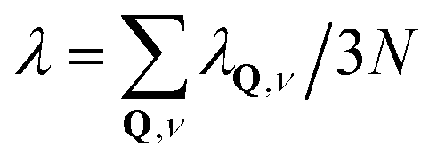 where N is the total number of atoms in the target and 3N is the total number of phonon modes.16
More recently, this inelastic theory has been more fully developed to include elastic as well as inelastic scattering where it is shown that a general expression for the DW exponent in terms of the e–ph interaction appears as2
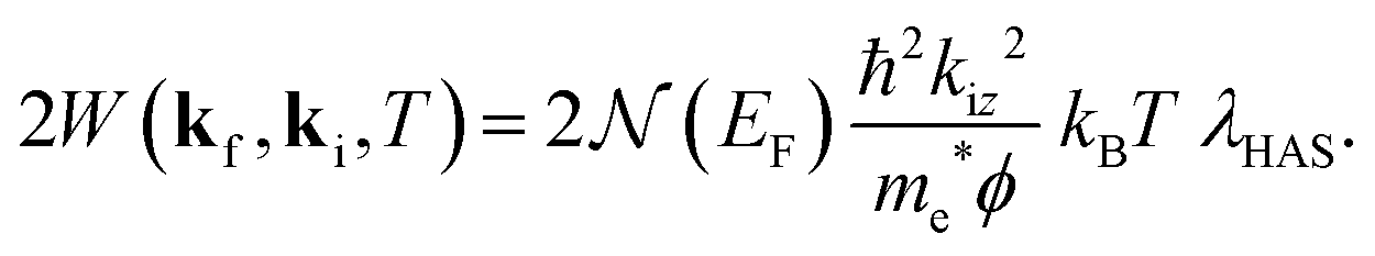
 | (3) |
 is the electronic density of electron states at the Fermi surface, me* is the electron effective mass and ϕ is the work function, kiz is the component normal to the surface of the incident atom wavevector in a specular scattering geometry, ω0 is an average phonon frequency, and nBE(ω0,T) is the Bose–Einstein function for a phonon of frequency ω0 at temperature T. With λHAS it is meant λ as derived from HAS DW measurements.
The simplest assumption is to expand the Bose–Einstein function to first order where it takes the value ħωQ,ν/kBT, an assumption that depends on all phonon energies being less than the temperature, ħωQ,ν < kBT. The DW exponent then becomes
 | (4) |
Since only low energy phonon modes are included, eqn (4) is linear in T and expressed in terms of the e–ph coupling constant λHAS. Eqn (4) has been successfully used to obtain values of λHAS for a large number of conducting surfaces including simple metals, metallic overlayers, chalcogenides and topological surfaces.3–5
If it is assumed that the entire phonon spectrum is dominated by a single dispersionless optical frequency ω0 then eqn (3) is written again for clarity
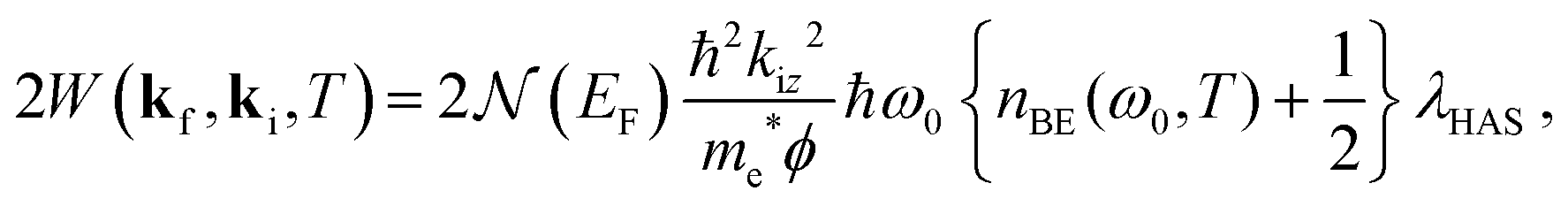 | (5) |
Eqn (5) has been used to extract values of λHAS for a variety of systems in which single-layer graphene is supported on metal substrates.11 The case of graphene is a bit unusual in that it has the usual low energy acoustic modes, but also has very high energy optical modes. Calandra and Mauri have shown that the optical modes of graphene make an important contribution to the e–ph constant λ and they suggested as a good approximation the assumption that the important optical modes can be represented by a single frequency ħω0 = 160 meV.17
For a surface 2D free-electron gas we can write 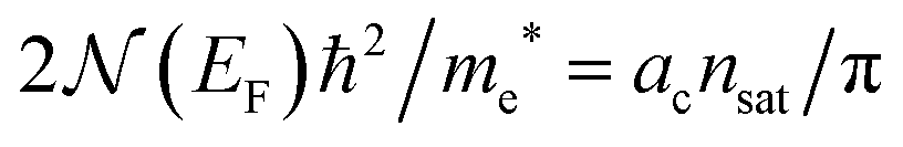 , with nsat being the number of surface layers contributing to the surface electron–phonon interaction and ac the area of the surface unit cell. The HAS DW exponent becomes
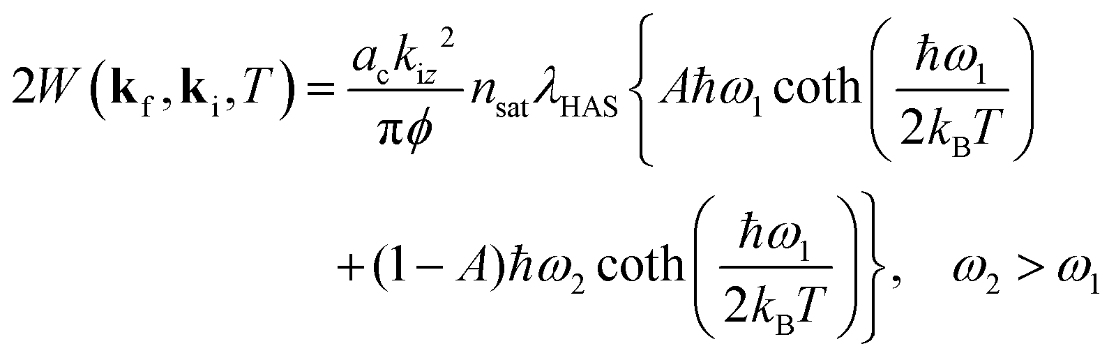 | (6) |
Note that for ω2 ≫ ω1 such that there is a temperature domain where ħω2/2kB ≫ T ≫ ħω1/2kB, the first term in graph parenthesis can be approximated by 2kBTλ1, while the second term is approximately constant
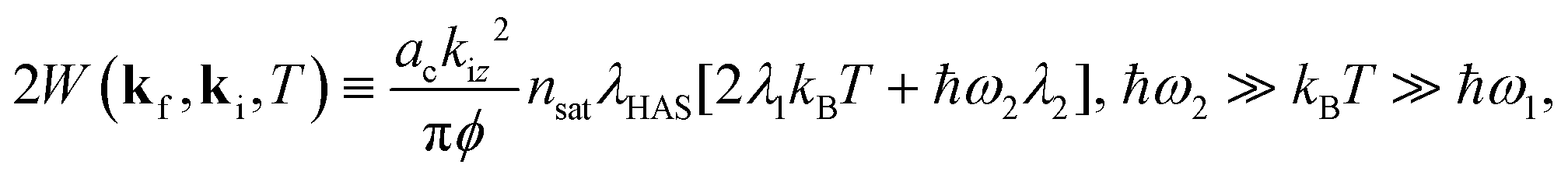 | (7) |
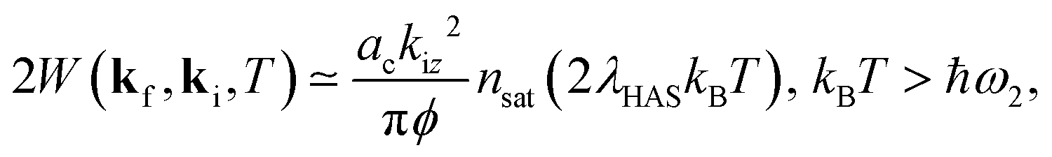 | (8) |
3 Examples of DW exponents that are non-linear in Temperature from He atom scattering
3.1 Optical versus acoustic phonons
In the case of conductor surfaces with more than one atom per unit cell and a clear separation between high-energy optical phonons and low-energy phonons (whether acoustic or optical), an increase of slope of 2W(kf,ki,T) or 2W(T) in order to simplify the notation is observed in the intermediate temperature region according to eqn (7). This is illustrated for Sb(111) and Bi(111) in Fig. 1.18 For these crystals, with two atoms per unit cell, there is a gap between the surface optical phonons and the surface acoustic phonons.19,20 The experimental specular HAS data actually show a slight deviation from linearity in the intermediate temperature region, which can however be appreciated by comparing the best fits with only the optical phonons (red lines), centered around 18 meV for Sb(111)19 and 14 meV for Bi(111)20 to those with only acoustic phonons, centered around 7 meV for Sb(111)19 and 4 meV for Bi(111).20 The fits with nsat = 4.7 for Sb(111), nsat = 4.5 for Bi(111), and only optical modes reproduce the experiments at all measured temperatures, whereas the fits with the acoustic modes start deviating below about 200 K (equivalent to ∼17 meV) for Sb(111) and 150 K (∼ 13 meV). In these materials it can be concluded that the values of λHAS (0.28 and 0.57, respectively3), previously derived from 2W(T) in the linear approximation, are mostly due to the surface optical modes. This is consistent with the observation of comparatively intense inelastic HAS peaks in the optical region of both surfaces.20,21 A more quantitative conclusion about the actual weights of acoustic and optical modes in the total mass-enhancement factor would require much smaller error bars in the HAS 2W(T) data, than those reproduced in Fig. 1, e.g., as it would be possibly obtained with 3 He spin-echo spectroscopy.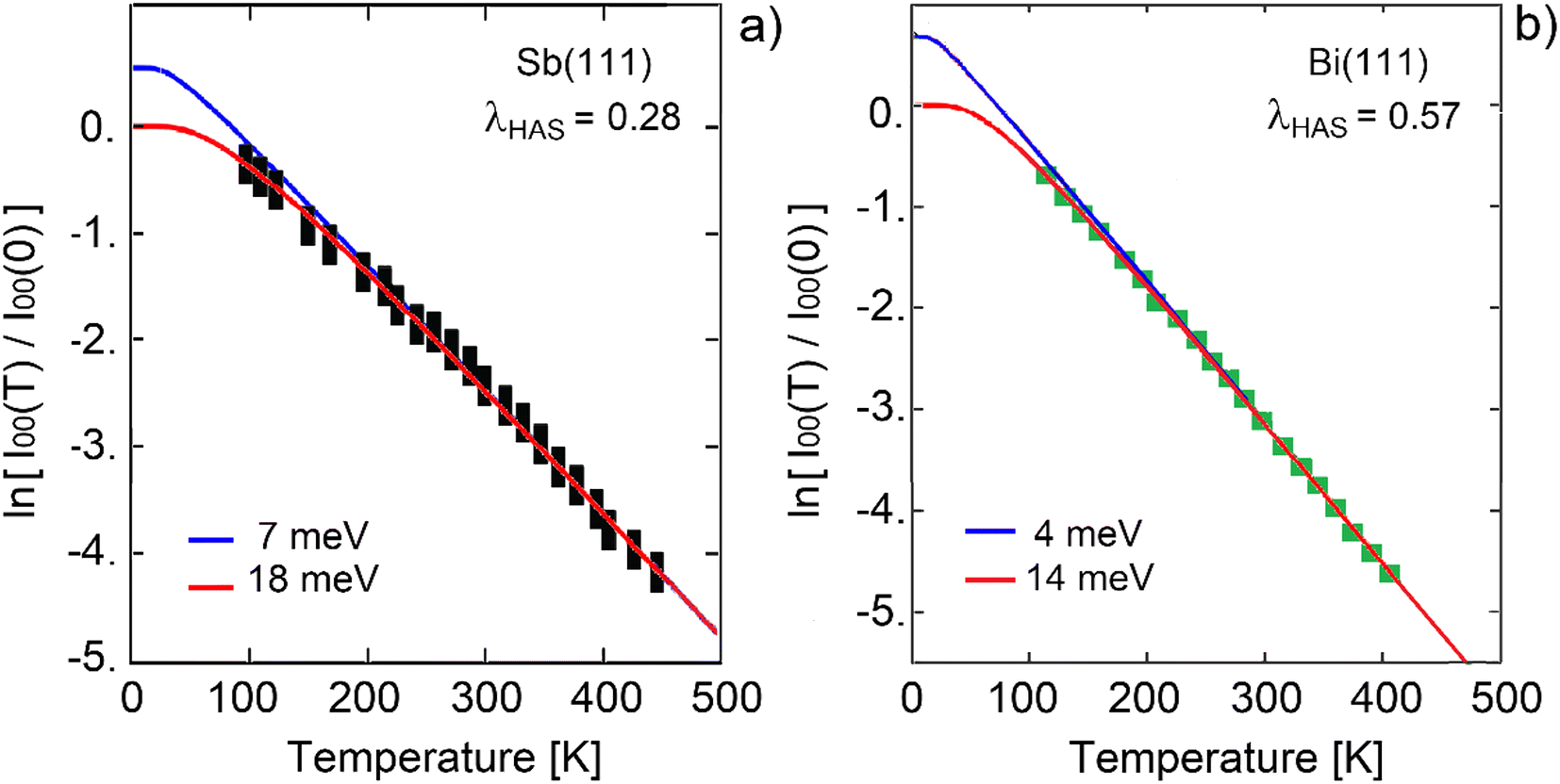 | ||
| Fig. 1 The DW exponent as a function of surface temperature for the specular diffraction peak of He atom scattering from Sb(111) and Bi(111).18 The incident energy is Ei = 24 meV and the specular angle is 45.75°. For Sb(111) we have λacoustic + λoptical = λHAS = 0.28 and for Bi(111), λHAS = 0.57. The best fits including only optical phonons (red lines), of average energy of 18 meV for Sb(111) and 14 meV for Bi(111), reproduce better the HAS data than those including only acoustic phonons (blue curves) of maximum energy of 7 and 4 meV, respectively. This qualitatively shows the dominant role of optical phonons in the electron–phonon interaction. | ||
3.2 He atom scattering from Sb2Te3 (111): which optical phonons?
The DW plot has been measured for Sb2Te3 (111) as shown in Fig. 2 and this provides an interesting view to illustrate the way that high energy phonon modes enter into the contributions to the e–ph coupling constant for a polyatomic conducting surface.10,22 The measurements were made at an incident He atom energy Ei = 17.42 meV and at a specular angle of θi = 45.75°.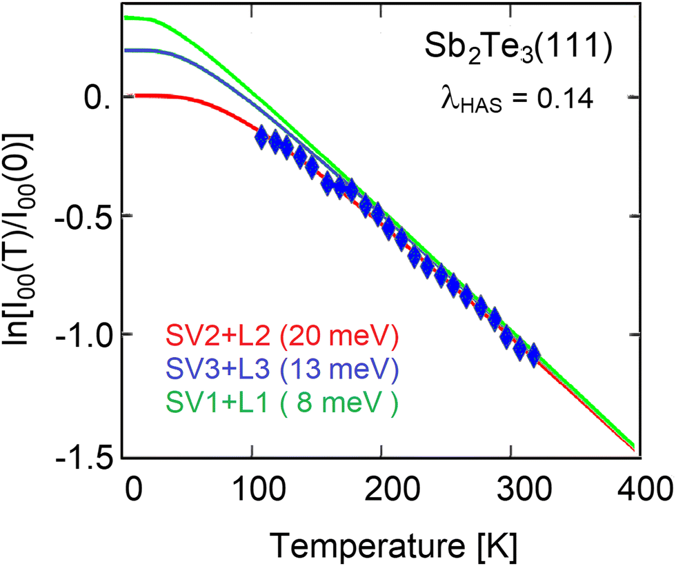 | ||
| Fig. 2 The DW exponent as a function of surface temperature for the specular diffraction peak of He atom scattering from Sb2Te3 (111). Data from ref. 22. The best fit including only the highest optical phonon branches SV2 and L2 involving the Sb layers (see ref. 23) (average energy 20 meV, red line) represents better the HAS data than the fits with only the lower optical branches SV3 and L3 mostly involving the central Te layer (average energy 13 meV, blue line), or only the acoustic branches SV1 and L1 at a maximum energy of 8 meV (green line), although the latter modes move mostly the top Te atoms at the surface layer. | ||
In this case, the surface phonon spectrum as obtained from ab initio DFPT calculations23 and observed by inelastic HAS22 can be reasonably well split in three regions where the surface phonons are mostly detected by HAS: a high-energy optical phonon region (∼20 meV), with large phonon displacements in the second (Sb) layer in both shear-vertical (SV2) and longitudinal (L2) directions; an intermediate optical phonon region (∼13 meV) with displacements more localized on the third atomic (Te) layer (SV3 + L3), and a low-energy, prevalent acoustic phonon region, centered at ∼8 meV, with larger displacements on the surface atomic layer (SV1 + L1). Also in this case the best fits with nsat = 12, corresponding to a Thomas-Fermi screening length extending to about 6 quintuple layer22 and only high-energy, intermediate-energy, or low-energy phonons shows that the total mass-enhancement factor derived from a pure linear fit, λHAS = 0.1410 is mostly due to the electron–phonon interaction involving the motion of Sb ions within the surface quintuple layer (SV2 and L2 phonon branches23). Again, the departure of the fits based on only intermediate- and low-energy phonons from experiment and from the good fit with only high-energy optical phonons starts at about 180 K, which corresponds to ∼16 meV and just separates the SV2 + L2 from the SV3 + L3 spectral regions.23
3.3 Overlayers: the role of substrate
It is now interesting to extend this analysis to the case of soft metal overlayers on a stiffer substrate. An interesting question is whether the e–ph interaction of the metal overlayer, basically related to its electron band-structure at the Fermi level, receives a contribution from the stiffer, high-energy phonons borrowed from the substrate. The temperature dependence of the HAS Debye–Waller exponent measured for Cs(110) ultrathin films on a Cu(111) overlayer for a growing number n of Cs atomic layers in Fig. 3,2,24 and similarly for Pb(111) ultrathin films also on a Cu(111) substrate2,25 in Fig. 4, actually provides evidence for this effect.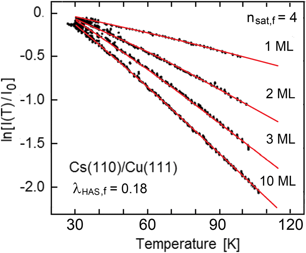 | ||
| Fig. 3 The DW exponent as a function of surface temperature for the specular diffraction peak of He atom scattering from multiple layers of Cs on Cu(111). The specular angle is θi = 50.5° and the incident energy is Ei = 28.5 meV. Data (black dots) are from for Cs overlayers of thickness n = 1, 2, 3, 10 ML on Cu(111) ref. 4 and 24. With λHAS,f = 0.18 and λHAS,s = 0.19 given for Cs and Cu in ref. 2 (Tables 3 and 2), respectively, and nsat,f = 4 for Cs films on Cu(111),2 the best fits (red curves) with eqn (6) and the substitutions of eqn (10) and (11) are obtained with the An = 0.84 (n = 1) and 1 (n > 1), and a substrate nsat,s = 5. | ||
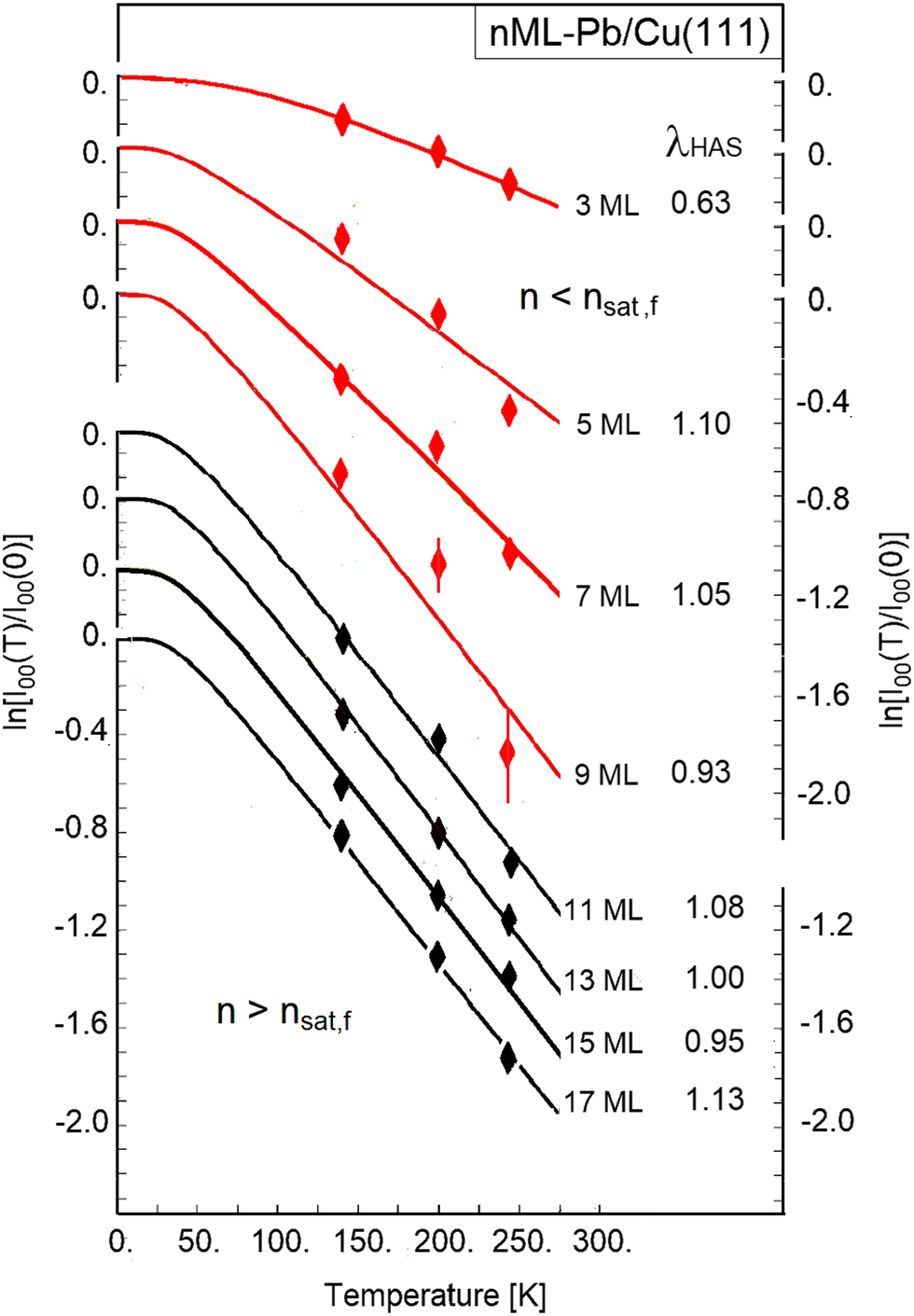 | ||
| Fig. 4 The DW exponent as a function of surface temperature for the specular diffraction peak of He atom scattering from multiple layers of Pb on Cu(111) for odd values of n from 3 to 17. The specular angle is θi = 45° and the incident energy is Ei = 5.97 meV. With an nsat,f of about 9, are also reasonably well fitted, within the fairly large experimental error, by eqn (6), (10) and (11) for both n < nsat,f (red data-points and lines) and n > nsat,f (black data-points and lines), and for the same nsat,s = 5 used for the Cs films on Cu(111). | ||
Both examples show that the slope of 2W(T) versus temperature increases with the number n of the atomic layers as long as it does not exceed the saturation number of the film, nsat,f.3 This is due to the increase with n of the number of electronic states at the Fermi level of the film (see, e.g., ref. 25) as well as of the number of its phonon modes. On the other hand, by considering that the saturation number represents the range from (and normal to) the surface of the e–ph interaction, when n<nsat,f the substrate layers near the interface will also contribute to the surface electron–phonon coupling, and for n = 0 the saturation number should just become that of the substrate surface, nsat,s. Thus, in order to discuss a possible role of the substrate in the actual value of λHAS, we introduce an n-dependent saturation number nsat(n) interpolating nsat,f for n ≥ nsat,f to nsat,s for n = 0,
| nsat(n) = nsat,s + (nsat,f − nsat,s)min(n/nsat,f,1). | (9) |
Clearly, nsat(nsat,f) = nsat,f and nsat(0) = nsat,s. On this basis, we adapt eqn (6) to the case of supported ultra-thin films with the substitutions
| λHASnsA → λHAS,fmin(n,nsat(n))An/dn ≡ λf(n), |
| λHASns(1 − A) → λHAS,s(nsat(n) − n)(1 −An)/dn ≡ λs(n), | (10) |
| dn = min(n,nsat(n))An + (nsat(n) − n)(1 − An), | (11) |
| λHAS(n) = λf(n) + λs(n). | (12) |
It is easily seen that this is what is directly obtained from the HAS-DW data for each thickness n, and that λHAS(nsat,f) = λHAS,f, and λHAS(0) ≡ λHAS,s.
Fig. 3 displays the experimental data for the HAS DW exponent 2W(T) (black dots) for Cs overlayers of thickness n = 1, 2, 3, 10 ML on Cu(111).4 The single Cs monolayer on Cu(111) behaves as a wetting layer, with a SV phonon frequency of ωf1 = 6.5 meV,26 which is larger than the maximum frequency of Cs (ωf = 4.3 meV25) here adopted for the films with n > 1. For the substrate we use the highest surface mode (S2) average frequency of 28 meV.27 With λHAS,f = 0.18 and λHAS,s = 0.19 given for Cs and Cu in ref. 2 (Tables 3 and 2), respectively, and nsat,f = 4 for Cs films on Cu(111),2 the best fits (red curves) with eqn (6) and the substitutions of eqn (10) and (11) are obtained with the An = 0.84 (n = 1) and 1 (n > 1), and a substrate nsat,s = 5. The latter value is considerably smaller than the value for the free Cu(111) surface, ns = 8.5, in ref. 2 (Table 2), which can be attributed to the charge transfer from the film due to the work function difference. The sequence of the best-fit values of An for n > 1 indicates a full independence (decoupling) of the Cs film e–ph interaction of (from) the high-energy substrate vibrations. This is reflected in the sequence of λHAS(1), which are all equal to the saturation value 0.18, except for λHAS(n) which is slightly larger. This agrees with the approximate linearity with n < nsat of the parameter α2, observed in Fig. 3(b) and 5(b) for thin alkali films on different transition-metal substrates.
This is not so for Pb films grown on Cu(111). The experimental HAS data for the DW exponent plotted in Fig. 4 as a function of temperature for odd values of n from 3 to 17 (the Pb films, after forming a wetting monolayer, tend to grow as a bilayer sequence2) with an nsat,f of about 9, are also reasonably well fitted, within the fairly large experimental error, by eqn (6), (10) and (11). This holds for both n < nsat,f (red data-points and lines) and n > nsat,f (black data-points and lines), and for the same nsat,s = 5 used for the Cs films on Cu(111). In this case the highest average optical surface phonon frequency of Pb layers (∼9 meV28) is used for ωf, while for λHAS,f, whose experimental HAS value displays some oscillations above nsat an average saturation value of 1.1 is used. It appears that at n = 3 (An = 0.5), the contribution of the substrate phonon to the e–ph coupling of the Pb film is 50%, and therefore equal to that of the film optical phonons, and survives (10%, i.e., An = 0.9) for n > 3 up to saturation. The dynamical decoupling occurs above saturation. The observed oscillations of the experimental λHAS(n) for n > nsat are likely to be due to the quantum-size effect,29 rather than to a residual effect of substrate dynamics. The corresponding sequence of λHAS(n) turns out to be in remarkably good agreement with the experimental values, apart from the oscillations mentioned above. All the information required is collected in Table 1.
| n-Cs/Cu(111) | n-Pb/Cu(111) | ||||||||
|---|---|---|---|---|---|---|---|---|---|
| n | 1 | 2 | 3 | 10 | 3 | 5 | 7 | 9 | 11 |
| A n | 0.84 | 1. | 1. | 1. | 0.5 | 0.9 | 0.9 | 0.9 | 1. |
| λ f(n) | 0.11 | 0.18 | 0.18 | 0.18 | 0.52 | 1.05 | 1.08 | 1.1 | 1.1 |
| λ s(n) | 0.074 | 0. | 0. | 0. | 0.10 | 0.01 | 0. | 0. | 0. |
| λ HAS(n) | 0.184 | 0.18 | 0.18 | 0.18 | 0.62 | 1.06 | 1.08 | 1.1 | 1.1 |
| λ expHAS | 0.18 | 0.18 | 0.18 | 0.18 | 0.63 | 1.10 | 1.05 | 0.93 | 1.08 |
4 Conclusions
In this work we have analysed the deviations from linearity of the DW exponent as a function of temperature as observed in He atom scattering from conducting surfaces and shown them to be an effect of the prominence of optical surface phonons. For sufficiently large temperatures, meaning T comparable or greater than the Debye temperature, the DW exponent 2Weff(kf,ki,T) is essentially linear in T as in eqn (8). However, eqn (2) shows that all phonon modes which have polarization components parallel to Δk contribute, even high energy modes which are neglected in the standard treatments. Here it is demonstrated that the electron–phonon interaction method of treating the DW factor allows one to readily estimate the contributions of high energy phonon modes such as, for example, optical modes.One effect of including such high energy modes is that it can lead to non-linear behavior in 2Weff(kf,ki,T), e.g., different from the standard linear behavior exhibited in eqn (8). These conclusions are supported by calculations for five different surface target systems. These consist of two ordered metallic systems with non-Bravais lattices that contain optical modes in their phonon dispersion relations, one rather exotic layered system containing a single layer of graphene, and two systems involving multiple layered growth of the “soft” metals Cs and Pb deposited on a Cu(111) substrate. In all of these cases small non-linearities of 2Weff(kf,ki,T) can be explained by contributions due to high energy phonon modes. This work indicates that non-linear behavior as a function of T in the DW exponent at high temperature may, in some cases, be explained by the effects of high energy modes, e.g., optical modes, which are usually neglected.
Demonstrating a specific role of the substrate in determining the electron–phonon interaction of an ultrathin films clearly opens new possibilities in the design of superconducting nanostructures and nanodevices.
Conflicts of interest
There are no conflicts to declare.Acknowledgements
SMA would like to acknowledge support from the Fundación Humanismo y Ciencia.Notes and references
- I. Y. Sklyadneva, G. Benedek, E. V. Chulkov, P. M. Echenique, R. Heid, K.-P. Bohnen and J. P. Toennies, Mode-selected electron–phonon coupling in superconducting Pb nanofilms determined from He atom scattering, Phys. Rev. Lett., 2011, 107, 095502 CrossRef.
- J. R. Manson, G. Benedek and S. Miret-Artés, Atom scattering as a probe of the surface electron–phonon interaction at conducting surfaces, Surf. Sci. Rep., 2022, 77, 100552 CrossRef CAS.
- J. R. Manson, G. Benedek and S. Miret-Artés, Electron–phonon coupling strength at metal surfaces directly determined from the helium atom scattering Debye–Waller Factor, J. Phys. Chem. Lett., 2016, 7, 1016 CrossRef CAS PubMed ; Erratum: 2016, 7, 1691.
- G. Benedek, S. Miret-Artés, J. P. Toennies and J. R. Manson, Electron–phonon coupling constant of metallic overlayers from specular He-atom scattering, J. Phys. Chem. Lett., 2018, 9, 76 CrossRef CAS.
- G. Benedek, S. Miret-Artés, J. R. Manson, A. Ruckhofer, W. E. Ernst and A. Tamtögl, Origin of the electron–phonon interaction of topological semimetal surfaces measured with helium atom scattering, J. Phys. Chem. Lett., 2020, 11, 1927 CrossRef CAS PubMed.
- A. Ruckhofer, D. Campi, M. Bremholm, P. Hofmann, G. Benedek, M. Bernasconi, W. E. Ernst and A. Tamtögl, THz surface excitations and electron–phonon coupling in Bi2Se3(111) from helium atom scattering, Phys. Rev. Res., 2020, 2, 023186 CrossRef CAS.
- G. Anemone, M. Garnica, M. Zappia, P. Casado Aguilar, A. Al Taleb, C.-N. Kuo, C. S. Lue, A. Politano, G. Benedek, A. L. Vázquez de Parga, R. Miranda and D. Farías, Experimental determination of surface thermal expansion and electron–phonon coupling constant of 1T-PtTe2, 2D Mater., 2020, 7, 025007 CrossRef CAS.
- G. Benedek, J. R. Manson and S. Miret-Artés, The electron–phonon interaction of low-dimensional and multi-dimensional materials from he atom scattering, Adv. Mater., 2020, 32, 2002072 CrossRef CAS PubMed.
- G. Anemone, P. Casado Aguilar, M. Garnica, F. Calleja, A. Al Taleb, C.-N. Kuo, C. S. Lue, A. Politano, A. L. Vázquez de Parga, G. Benedek, D. Farías and R. Miranda, Electron–phonon coupling in superconducting 1T-PdTe2, npj 2D Mater. Appl., 2021, 5, 25 CrossRef CAS.
- G. Benedek, J. R. Manson, S. Miret-Artés, A. Ruckhofer, W. E. Ernst, A. Tamtögl and J. P. Toennies, Measuring the electron–phonon interaction in two-dimensional superconductors with He atom scattering, Condens. Matter, 2020, 5, 79 CrossRef CAS (2020). Erratum: Condens. Matter, 2021, 6, 54.
- G. Benedek, J. R. Manson and S. Miret-Artés, The electron–phonon coupling constant for single-layer graphene on metal substrates determined from he atom scattering, Phys. Chem. Chem. Phys., 2021, 23, 7553 RSC.
- B. Holst, G. N. Alexandrowicz, N. Avidor, G. Benedek, G. Bracco, W. E. Ernst, D. Farías, A. Jardine, J. R. Manson, R. Marquardt, S. Miret-Artés, A. Tamtögl, J. W. Wells and W. Allison, Material properties particularly suited to be measured with helium scattering: Selected examples from 2D materials, van der Waals heterostructures, glassy materials, catalytic substrates, topological insulators and superconducting radio frequency materials, Phys. Chem. Chem. Phys., 2021, 23, 7653 RSC.
- G. Benedek and J. P. Toennies, Atomic scale dynamics at surfaces: Theory and experimental studies with helium atom scattering, Springer Series in Surface Sciences, Springer Press, Heidelberg, 2018, vol. 63, ISBN 978-3-662-56443-1 Search PubMed.
- Springer Series in Surface Sciences, ed. E. Hulpke, Springer Press, Heidelberg, 1992, vol. 27 Search PubMed.
- G. Benedek, M. Bernasconi, K.-P. Bohnen, D. Campi, E. V. Chulkov, P. M. Echenique, R. Heid, I. Yu. Sklyadneva and J. P. Toennies, Unveiling mode-selected electron–phonon interactions in metal films by helium atom scattering, Phys. Chem. Chem. Phys., 2014, 16, 7159 RSC.
- P. B. Allen, Neutron spectroscopy of superconductors, Phys. Rev. B: Solid State, 1972, 6, 2577 CrossRef CAS.
- M. Calandra and F. Mauri, Electron–phonon coupling and electron self-energy in electron-doped graphene: Calculation of angular-resolved photoemission spectra, Phys. Rev. B: Condens. Matter Mater. Phys., 2007, 76, 205411 CrossRef.
- A. Tamtögl, M. Mayrhofer-Reinhartshuber, P. Kraus and W. E. Ernst, Surface Debye temperature and vibrational dynamics of antimony (111) from helium atom scattering measurements, Surf. Sci., 2013, 617, 225 CrossRef.
- D. Campi, M. Bernasconi and G. Benedek, Phonons and electron–phonon interaction at the Sb(111) surface, Phys. Rev. B: Condens. Matter Mater. Phys., 2012, 86, 075446 CrossRef.
- A. Tamtögl, P. Kraus, M. Mayrhofer-Reinhartshuber, W. E. Ernst, D. Campi, M. Bernasconi and G. Benedek, Surface and sub-surface phonons of Bi(111) measured with helium atom scattering, Phys. Rev. B: Condens. Matter Mater. Phys., 2013, 87, 035410 CrossRef ; Erratum: Phys. Rev. B, 2013, 87, 159906.
- A. Tamtögl, P. Kraus, M. Mayrhofer-Reinhartshuber, G. Benedek, M. Bernasconi, D. Dragoni and W. E. Ernst, Surface phonons and CDW excitations by helium atom scattering from Sb(111), npj Quantum Mater., 2019, 4, 28 CrossRef.
- A. Ruckhofer, S. Halbritter, H. E. Lund, A. Julie, U. Holt, M. Bianchi, M. Bremholm, G. Benedek, P. Hofmann, W. E. Ernst and A. Tamtögl, Inelastic helium atom scattering from Sb2Te3(111): Surface phonon dispersion, kinematical focusing and surfing, Phys. Chem. Chem. Phys., 2021, 23, 7806 RSC.
- D. Campi, M. Bernasconi and G. Benedek, Ab initio calculation of surface phonons at the Sb2Te3(111) surface, Surf. Sci., 2018, 678, 38 CrossRef.
- E. Hulpke, J. Lower and A. Reichmuth, Strain and confined resonances in ultrathin alkali-metal films, Phys. Rev. B: Condens. Matter Mater. Phys., 1996, 53, 13901 CrossRef CAS.
- D. Campi, M. Bernasconi, G. Benedek, A. P. Graham and J. P. Toennies, Surface lattice dynamics and electron–phonon interaction in cesium ultra-thin films, Phys. Chem. Chem. Phys., 2017, 19, 16358 RSC.
- J. P. Gauyacq and A. K. Kazansky, Laser-induced vibrational excitation and desorption in the Cs/Cu(111) and Na/Cu(111) systems, Surf. Sci., 2007, 601, 5473 CrossRef CAS.
- G. Benedek, M. Bernasconi, V. Chis, E. Chulkov, P. M. Echenique, B. Hellsing and J. P. Toennies, Theory of surface phonons at metal surfaces: Recent advances, J. Phys.: Condens. Matter, 2010, 22, 084020 CrossRef CAS PubMed.
- J. Braun, P. Ruggerone, G. Zhang, J. P. Toennies and G. Benedek, Surface phonon dispersion curves of thin Pb films on Cu(111), Phys. Rev. B: Condens. Matter Mater. Phys., 2009, 79, 205423 CrossRef.
- B. J. Hinch, C. Koziol, J. P. Toennies and G. Zhang, Evidence for quantum size effects observed by helium atom scattering during the growth of Pb on Cu(111), Europhys. Lett., 1989, 10, 341 CrossRef CAS.
| This journal is © the Owner Societies 2022 |