
 Open Access Article
 This Open Access Article is licensed under a Creative Commons Attribution-Non Commercial 3.0 Unported Licence
Temperature-induced polymorphism of a benzothiophene derivative: reversibility and impact on the thin film morphology†
Shunya
Yan
a,
Alba
Cazorla
 a,
Adara
Babuji
a,
Eduardo
Solano
b,
Christian
Ruzié
c,
Yves H.
Geerts
cd,
Carmen
Ocal
*a and
Esther
Barrena
*a
a,
Adara
Babuji
a,
Eduardo
Solano
b,
Christian
Ruzié
c,
Yves H.
Geerts
cd,
Carmen
Ocal
*a and
Esther
Barrena
*a
aInstitut de Ciència de Materials de Barcelona (ICMAB-CSIC), 08193 Bellaterra, Barcelona, Spain. E-mail: e.barrena@csic.es; cocal@icmab.es
bALBA synchrotron, C/de la Llum 2-26, Cerdanyola del Vallès, Barcelona, 08290, Spain
cLaboratoire de Chimie des Polymères, Faculté des Sciences, Université Libre de Bruxelles (ULB), Boulevard du Triomphe, CP 206/01, 1050 Bruxelles, Belgium
dInternational Solvay Institutes of Physics and Chemistry, Université Libre de Bruxelles (ULB), Boulevard du Triomphe, CP 231, 1050 Bruxelles, Belgium
First published on 4th October 2022
Abstract
The identification of polymorphs in organic semiconductors allows for establishing structure-property relationships and gaining understanding of microscopic charge transport physics. Thin films of 2,7-bis(octyloxy)[1]benzothieno[3,2-b]-benzothiophene (C8O–BTBT–OC8) exhibit a substrate-induced phase (SIP) that differs from the bulk structure, with important implications for the electrical performance in organic field effect transistors (OFETs). Here we combine grazing incidence wide-angle X-ray scattering (GIWAXS) and atomic force microscopy (AFM) to study how temperature affects the morphology and structure of C8O–BTBT–OC8 films grown by physical vapor deposition on SiO2. We report a structural transition for C8O–BTBT–OC8 films, from the SIP encountered at room temperature (RT) to a high temperature phase (HTP) when the films are annealed at a temperature T ≥ 90 °C. In this HTP structure, the molecules are packed with a tilt angle (≈39° respect to the surface normal) and an enlarged in-plane unit cell. Although the structural transition is reversible on cooling at RT, AFM reveals that molecular layers at the SiO2 interface can remain with the HTP structure, buried under the film ordered in the SIP. For annealing temperatures close to 150 °C, dewetting occurs leading to a more complex morphological and structural scenario upon cooling, with coexistence of different molecular tilts. Because the molecular packing at the interface has direct impact in the charge carrier mobility of OFETs, identifying the different polymorphs of a material in the thin film form and determining their stability at the interfaces are key factors for device optimization.
Introduction
Organic semiconductor (OSC) thin films based on π-conjugated molecules are of enormous interest as active components for electronic devices. The field has seen radical improvements in the last decades with an increasing number of products in the marketplace such as the organic light-emitting diode (OLED) display technology.1,2 The development of organic field effect transistors (OFETs) has not been as fast as for OLEDs and although OFETs have become a commercially viable technology, many issues related to fundamental research still remain elusive.3,4 The charge carrier mobility, which is one of the main performance metrics for OFETs, relies on structural details at different length scales that are not yet fully understood and satisfactorily controllable.5–8 The crystalline structure adopted by small conjugated molecules is hold by weak intermolecular van der Waals interactions, which confer to the OSC materials a high degree of polymorphism. The identification of new or specific polymorphs allows for establishing structure-property relationships and gaining an understanding of microscopic charge transport physics. In addition, polymorphism can represent an added value as it provides access via growth conditions to metastable phases, otherwise inaccessible under equilibrium conditions.9 In particular, the solid-surface on which a thin film grows, can give rise to surface-induced polymorphism.10 Hence, for thin films of some molecular materials it is observed that the substrate stabilizes a molecular packing that is different from the bulk structure. The so-called thin-film phase of pentacene is the best-known example of surface-induced phase (SIP).10–13 Because the degree of crystalline order and morphology of on-surface developed structures are influenced by both, kinetic and thermodynamic factors, the optimization of thin film OFETs requires exploring different growth parameters, including substrate temperature during growth. As the molecular packing crucially determines the properties of a material, polymorphism can have a direct impact on the functional properties and time stability of devices.14Alkylated BTBT derivatives (Cn–BTBT–Cn) exhibit a high carrier mobility (3–20 cm2 V−1 s−1),15–19 which has been related to their tendency to grow on the SiO2 surface forming well-ordered layers of standing molecules with a herringbone (HB) arrangement of the BTBT cores.20 The crystalline packing in the thin-film state is similar to that in the bulk single crystals.18,21,22 For 2,7-dioctyloxy[1]benzothieno[3,2-b]benzothiophene (C8O–BTBT–OC8), with an oxygen atom added between the BTBT and each alkyl chain, important structural differences are found. The thermodynamically stable crystalline phase (single-crystal structure) consists of a triclinic structure with two molecules per unit cell exhibiting a co-facial stacking in which adjacent molecules are displaced respect to each other along the c-axis.21,23,24 In thin films, however, the presence of a SIP structure has been reported, which consists of a lamellar arrangement of the molecules with herringbone packing of the BTBT cores within the lamellae.23–26 The reported SIP for C8O–BTBT–OC8 is isostructural with the C8–BTBT–C8 structure.10 A difference from the bulk phase, which presents an inter-digitation of the alkyl chains, the (001) plane of the SIP conforms to a flat substrate surface. The HB structure of C8O–BTBT–OC8 has been observed to form on surfaces for films prepared from vapour deposition26 as well as from solution processing.14,23–25 A charge carrier mobility about 1 cm2 V−1 s−1 has been reported for OFETs based on thin films presenting the SIP phase.14 Although this mobility is lower than that reported for C8–BTBT–C8 OFETs, the investigation of the electrical properties has been scarce and there is possible room for improvement via processing or post-processing methods (e.g., solvent or thermal annealing). Previous studies have reported that time or solvent vapour annealing lead to a conversion towards the bulk structure,24 indicating that the SIP is metastable. The effect of temperature as a parameter has not yet been explored.
In this work, we combine synchrotron Grazing-Incidence Wide-Angle X-ray Scattering (GIWAXS) and Atomic Force Microscopy (AFM) to characterize the films grown by physical vapour deposition on the native oxide surface of p-doped Si wafers. We investigate the effect of temperature, either by using different substrate temperatures during the growth or by post-annealing treatments of films deposited at room temperature (RT).
Experimental section
GIWAXS experiments were performed at the BL11-NCD-SWEET beamline of the ALBA Synchrotron (Spain) using a photon energy of hν = 12.4 keV. Different incident angles were used, ranging between 0.09° and 0.15°, ensuring measurements with surface sensitivity or full thin film penetration while minimizing the substrate contribution. A large-area 2D Rayonix LX 255-HS detector, which consists of a pixel array of 2880 × 960 (V × H) with a pixel size of 88.54 × 88.54 μm2 for the binning employed, was used to capture 2D images of the diffraction patterns. The scattering vector (q) was calibrated using Cr2O3 as a calibration standard and pyFAI python library.28 To improve the signal-to-noise ratio and to check beam damage, 50 images with an exposure time of 0.02 s were acquired and summed up at each temperature and for each incident angle. The conversion of the data to the reciprocal space was performed by using a developed python routine, obtaining the out-of-plane (OOP), qz, and in-plane (IP), qxy, components of the scattering vector corresponding to the directions perpendicular and parallel to the surface, respectively. Because of the grazing incidence geometry, a section cut obtained along the vertical direction of the detector (so-called OOP section cuts in the text) is not the real specular scan. 2D GIWAXS patterns of annealed samples were collected in situ using the available Linkam TMS600 heating stage adapted for grazing incidence experiments to monitor the structural changes. Scattering patterns were recorded under N2 gas flow with a step-wise temperature profile, which consisted of a fast heating ramp (150 °C min−1) and 5 minutes of annealing time before data collection. A set of twin samples was annealed in a heating plate (5 minutes annealing time in ambient conditions) and measured at room temperature by AFM. In the extraction of the lattice parameters we have considered the uncertainty given by the error propagation in the equation, considering the uncertainty of the peak position, i.e., the error of the Gaussian fit for each peak. In this way the obtained uncertainty is <0.0008 Å for b and <0.02 Å for a.C8O–BTBT–OC8 was synthesized as previously reported.21,24 Before films growth, the silicon substrates (Si-Mat, Germany) were cleaned by sonication in acetone and ethanol, for 10 minutes in each solution, and degassed in vacuum (∼10−6–10−7 mbar) for 15 minutes at 250 °C. The thin films of C8O–BTBT–OC8 were grown by physical vapour deposition in the same vacuum chamber, the growth rate and film thickness were about 2–3 Å min−1 and 14 nm, respectively, as monitored by a quartz crystal microbalance (QCM). For post-growth annealing the samples were kept 5 minutes at the desired temperature.
AFM measurements in contact and dynamic modes were performed at RT using a commercial instrument (Cypher ES, Oxford instruments). For contact mode, silicon nitride tips were used (cantilevers with a nominal spring constant k = 0.02 or 0.03 N m−1 from Bruker) whereas for dynamic mode we used Cr/Pt-coated silicon tips (cantilevers with a nominal spring constant k = 3 N m−1, from BudgetSensors). AFM data we analyzed with AR SPM Software from Oxford Instruments and WxSM freeware27 from Nanotech Electronica.
Results
1. Structural analysis by GIWAXS
Thin films of C8O–BTBT–OC8 (thickness ≈14 nm) were deposited by physical vapour deposition in vacuum on silicon wafers at RT. The film structure was measured by GIWAXS during post-growth stepwise annealing of the sample (see the Experimental section). Fig. 1a displays 2D GIWAXS patterns acquired at different temperatures (patterns for other temperatures are displayed in Fig. S1, ESI†). Section cuts along the OOP and IP directions are provided in Fig. 1b and c, respectively.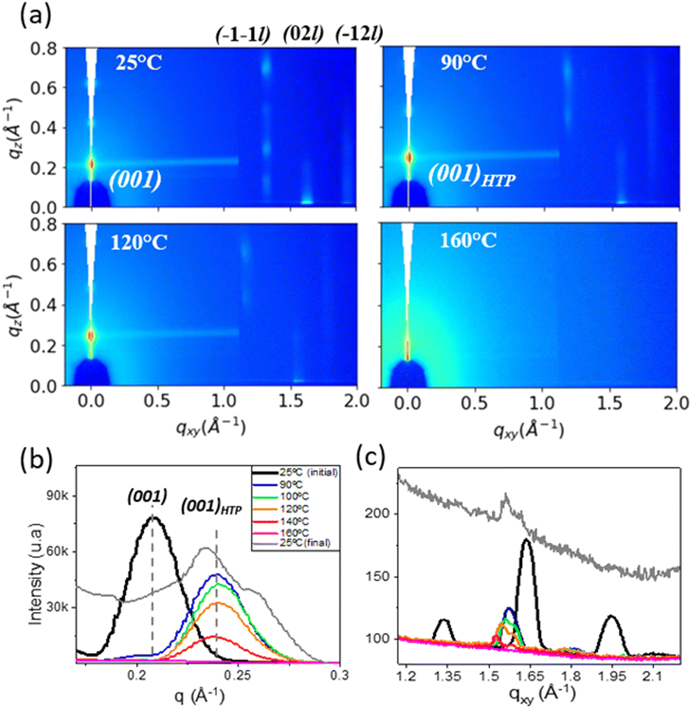 | ||
| Fig. 1 (a) 2D GIWAXS patterns of a C8O–BTBT–OC8 thin-film (incidence angle of 0.13°) acquired at the indicated temperatures. The horizontal line appearing at qz ≃ 0.24 Å−1 is produced by the CCD camera blooming due to the high intense signal of the (001) peak. Line cuts along the out-of-plane (b) and in-plane (c) directions. Additional 2D GIWAXS patterns and OOP cuts (larger q range) are provided in Fig. S1 (ESI†) for all employed temperatures. The data acquired at RT after annealing the film at 160 °C in (b) and (c) have been multiplied by a factor of 5 (grey lines). | ||
The diffraction pattern measured at RT agrees with the reported HB structure for the C8O–BTBT–OC8 SIP, oriented with the (001) plane parallel to the surface. The (001) crystalline plane in the SIP forms a flat and compact surface formed by densely packed alkyl chains that is stabilized by the flat surface. In the 2D GIWAXS pattern of Fig. 1a, the scattering intensity visible at qxy ≃ 1.33 Å−1, 1.64 Å−1 and 1.95 Å−1 have been indexed as (−1−1l), (02l) and (−12l), respectively. Such pattern, with the absence of scattering intensity for (10l) or (02l), is indicative of an in-plane rectangular cell (γ = 90°) with two molecules per unit cell. The in-plane deduced unit cell (Table 1) agrees with the previously reported,10 but with a slightly lower value of the b-lattice parameter (<1%). The Bragg peak position in the OOP direction (q = 0.204 Å−1) has an associated inter-planar spacing of d = 30.8 Å in agreement with previous reports, although the (001) Bragg peak appears at a slightly larger q-position (Fig. S1 in ESI†). The average molecular tilt respect to the surface normal, estimated from the molecular length (L = 33.88 Å) and the inter-planar distance results in θ ≃ 24°, corresponding to the tilt of the alkyl chains in this structure.24
| C8O–BTBT–OC8 (SIP) | C8O–BTBT–OC8 (HTP) | |
|---|---|---|
| Crystal system | Monoclinic | Monoclinic |
| a (Å) | 6.02 | 7.05 |
| b (Å) | 7.66 | 7.87 |
| c (Å) | 31.08 | 29.2 |
| α (°) | 90 | 90 |
| β (°) | 97 | 63.9 |
| γ (°) | 90 | 90 |
At a temperature of ≈90 °C, a remarkable change in the diffraction pattern points to the formation of a new polymorphic phase. Hereafter, this phase is referred to as the high temperature phase (HTP). As it can be appreciated in Fig. 1b, the structural transition involves a shift of the (001) Bragg peak to a larger q (q = 0.237 Å−1), which leads to dHTP ≈ 26.5 Å, a considerably reduced inter-planar spacing. In the 2D GIWAXS pattern still three rods are visible at qxy ≃ 1.17 Å−1, 1.58 Å−1 and 1.81 Å−1, i.e., shifted respect to those for the SIP structure (Fig. 1a and c). Note that the structural change is accompanied by a marked variation in the intensity distribution along qz. Although there are not enough independent Bragg diffraction peaks to determine the six lattice constants (a, b, c, α, β and γ) of the crystallographic unit cell, the analysis can be simplified by some reasonable assumptions. The absence of diffraction features in the low qxy region (i.e., absence of (10l) and (01l)) allows us to presume that the symmetry of the unit cell is preserved; therefore, the three rods can be indexed as (−1−1l), (02l) and (−12l). Under these assumptions, there are only four parameters to be determined in the monoclinic unit cell: a, b, c and β (the angle between c and a). The lattice parameters a and b can be directly extracted from the peak position of the (020) and the qxy component of the (−1−1l) rod; c and β are deduced from the qz component of the (−1−10) reflection (qz = 0.44 Å−1) and the (001) Bragg position. Further details are presented in the ESI.† The calculated lattice parameters are given in Table 1. The in-plane unit cell changes from aSIP = 6.02 Å and bSIP = 7.66 Å in the SIP to aHTP = 7.05 Å and bHTP = 7.87 Å in the HTP. The enlargement of the lattice parameter a and the reduction of the angle β are the most noticeable changes in the structural transition. Overall, the changes observed by GIWAXS are consistent with a scenario in which the molecules are tilted with respect to the surface normal. Notably, the intensity of the (02l) reflection remains in-plane while the scattering intensity in the (−1−1l) and (−12l) is enhanced out-of-plane, indicating that the molecules are tilted towards the a-axis. Given that the BTBT cores are the most electron-dense parts of the molecule, the observed intensity enhancement along the (−11l) and (−12l) rods can be interpreted as a sign of the tilt of the BTBT cores (not uniquely the alkyl chains). The average molecular tilt from the surface normal estimated from the molecular length and dHTP is θ ≃ 38.5°, without taking into account any possible tilt difference between core and alkyl chains.
We have used the GIDSimulator software29 to simulate the diffraction pattern with the extracted parameters for the HTP, obtaining the diffraction spots (Fig. 2a), which match with the recorded scattering pattern. The temperature induced structural transition from the SIP to the HTP is illustrated in Fig. 2b.
 | ||
| Fig. 2 (a) 2D diffraction pattern measured at 90 °C and simulated pattern (pink dots) for the HTP structure with the unit cell parameters given in Table 1. (b) Sketch illustrating the main changes involved in the structural transition from the SIP to the HTP structure with annealing temperature: tilting of the molecules and expansion of the a-lattice parameter. (c) Inter-planar spacing at different temperatures extracted from the (001) peak. After annealing, the film was cooled down and measured at 25 °C (final); the values appear with square symbols, the smaller size of one of them indicates the lower intensity of the corresponding peak (see Fig S2 in ESI†). | ||
The HTP remains visible for substrate temperatures above 90 °C. Nevertheless, the peaks show a visible reduction of the intensity beyond 100 °C (see Fig. 1b and c), a fact that indicates that some molecular desorption occurs induced by thermal annealing. The absence of diffraction features at 160 °C (pink lines) can be interpreted as the full desorption of the film and/or as a change into a disordered state. Indeed, measurements taken at RT, after cooling down the film, reveal the presence of fairly faint structural features, confirming the desorption of most of the film. The OOP intensity (grey line in Fig. 1b) shows two dominant peaks at qz = 0.235 Å−1 and 0.258 Å−1 (see fitting details in Fig. S2 in ESI†), corresponding to an interlayer spacing of 26.7 Å and 24.3 Å, respectively. This observation is interpreted as the coexistence of different tilt angles in the remaining molecular film. Furthermore, the in-plane data (grey line in Fig. 1c and Fig. S2, ESI†) shows a weak in-plane intensity at 1.58 Å−1 that gives evidence of a molecular layer with prevalence of the HTP structure. The values of the d001 spacing calculated at each temperature have been displayed in Fig. 2c.
In the following, we address the reversibility of the structural transition by AFM as well as the impact that the substrate temperature during growth has on the morphology of the films.
2. Thin film morphology analysis by AFM
Fig. 3a shows the surface morphology of a C8O–BTBT–OC8 thin film (14 nm nominal thickness) deposited on the SiO2 substrate at RT (25 °C). As it can be seen in the displayed images, the surface exhibits a quite laterally homogeneous morphology. The magnified image at the inset shows terraced islands with a round shape on top of a continuous film. Taking into account the QCM nominal thickness, the continuous film is estimated to be formed by four complete single molecular layers. A step height of 3.2 ± 0.1 nm is obtained (Fig. S3, ESI†), which is in agreement with the reported interlayer distance of the SIP structure.24 The consequences that post-growth annealing has on the film morphology can be seen in Fig. 3 for 100 °C (b), 130 °C (c) and 150 °C (d). We note that all AFM images were obtained after the sample was allowed to cool down at RT after each annealing treatment. | ||
| Fig. 3 AFM topographic images of 14 nm (nominal) of C8O–BTBT–OC8 deposited on SiO2 at RT (25 °C) (a) and after post-annealing during 5 min at diverse temperatures: 100 °C (b), 130 °C (c) and 150 °C (d). The lateral size of the large images is 30 μm × 30 μm and the dimensions of the image in the inset in (a) is 210 nm × 210 nm. The cartoons are schematic representations of the respective film morphology based on topographic profiles analysis of the images. Yellow color is associated to SIP (upright molecules) and green to tilted molecular layers. Note: all images were taken at RT. | ||
Several important changes in the morphology are observed for the sample post-annealed to 100 °C (Fig. 3b). On the one hand, the number of levels exposed at the film surface is lower than in the as-grown film. The height of the individual layers is the same as in as-deposited films, indicating that the structural transition observed by GIWAXS is reversible and that the HTP transforms back to the SIP structure after cooling down. On the other hand, the top-most layer consists of laterally extended islands that cover about 62% of the surface and shows small voids of one single layer depth. These holes might be the combined result of non-filled space after coalescence of the lateral growing regions and molecular desorption. This sort of flattening process is explained by an increased mobility of the molecules on the surface and a reduction of the Ehrlich–Schwoebel barrier when increasing the temperature.30 The post-annealing treatment done has a smoothening effect on the morphology. After annealing the film at 130 °C (Fig. 3c), a further lateral enlargement of the terraces (with lateral sizes surpassing tens of micrometres) is seen. Despite a large vertical scale arising from newly created pitches reaching the substrate (Fig. S4 in ESI†), few topographic levels are seen. Interestingly, the thickness of the film has decreased as determined by the pitches depth, which confirms the initiation of molecular desorption from the film. This observation is fully consistent with the observed decrease of scattering intensity in the GIWAXS pattern for annealing temperatures above ≈100 °C.
The surface morphology dramatically changed upon a post-annealing temperature of 150 °C (Fig. 3d). Large multi-layered mounds with a circular shape (domes) appear on the surface (labelled I), with a diameter of several micrometers and a height of some tens of nanometers. These domes cover only about 10% of the surface and are surrounded by a corona and a considerably flat surrounding film (labelled II). Such morphology is characteristic of a film dewetting process. The differences among these two regions are illustrated in Fig. 4. A magnification of the stepped side of one mound is shown in Fig. 4a. We first note that the exposed terraces at this multi-layered region have step heights varying between 2.6 and 2.9 nm, i.e., lower than the interlayer spacing of the SIP structure. This result is quantitatively illustrated in Fig. 4b, where the height distribution of the image recorded in region I is superimposed to a grid made out of vertical dotted lines separated by 3.2 nm, the interlayer distance measured for the RT film. This observation agrees with the GIWAXS data (Fig. 2c), confirming the coexistence of diverse tilted configurations after cooling the annealed C8O–BTBT–OC8 films. There is no clear correlation between the molecular tilt and the terrace level.
 | ||
| Fig. 4 AFM topographic images taken in region I (a) and region II (c) of the C8O–BTBT–OC8 film, at RT after being post-annealed at 150 °C (magnifed regions of Fig. 3d). (b) Height distribution of the image in (a), the vertical dotted lines every 3.2 nm serve as a reference to show that the diverse step heights deviate from the interlayer distance measured for the SIP structure. (d) Line profile corresponding to the blue segment in (c). | ||
As it can be seen in the corresponding magnification (Fig. 4c), region II is fairly flat, consisting of two film surface levels. The uncovered substrate is visible only through a few pinholes or voids (see white arrows in the figure), which allow us determining the layer thickness by topographic profile analysis (Fig. 4d). The molecular layer with the lowest height has a measured thickness that ranges between 2.3 and 2.8 nm, depending on the surface location. The highest level is ∼3.2 nm thick, as corresponds to that expected for the SIP structure. On the basis of the GIWAXS results, we suggest that these regions correspond to one single molecular layer at the film/SiO2 interface, that remains in the HTP structure when cooling from high temperature to RT, due to an incomplete transition from the HTP to the SIP. Since the SIP phase is denser than the HTP, voids are formed within the layer (white arrows). Moreover, the thinner molecular layer is easily removed due to the sweeping action of the tip while scanning in contact mode, likely indicating a defective packing (Fig. S5 in ESI†).
The impact that the morphological changes have on the surface roughness of the film has been analyzed in terms of the root mean square (RMS) calculated for large scale AFM topographic images (900 μm2) at the different post-annealing temperatures. The data depicted in Fig. 5a show that the roughness of the as-grown films (RMS = 3 nm) considerably decreases by more than 50% after post-annealing at 100 °C. For subsequent temperature treatments, a relatively low increase of RMS is seen, in accordance with the similar number of exposed levels (Fig. 3b–d). For the post-annealed samples at 150 °C, two values were estimated that correspond to areas including or excluding the tall round mounds (pink and blue symbols, respectively). A plot of the interlayer spacing (layer thickness) measured by AFM after post-annealing at different temperatures is presented in Fig. 5b. From the AFM results, we conclude that the HTP structure reverses to the SIP after cooling the films to RT if the annealing temperature is kept lower than that of the dewetting transition (≈150 °C).
 | ||
| Fig. 5 (a) Root mean squared (RMS) surface roughness for the as-grown sample at 25 °C and for post-annealed films at the indicated temperatures (all measured at RT). The pink symbol corresponds to an area including the multilayer mound of region I of the sample post-annealed at 150 °C. (b) Height of single molecular layers obtained from AFM topographical images after post-annealing at different temperatures (the estimated error is ±0.1 nm). | ||
In order to gain insight into the role of temperature as a growth parameter, we next analyze the morphology of thin films grown at different substrate temperatures and measured after cooling down to RT. Here the thickness of the films is found to be similar for all the growth temperatures. We note that sample cooling down inside the high vacuum chamber takes place with a lower rate than in the post-annealing experiments. In Fig. 6, the morphology obtained for thin films grown at 25 °C (a), 85 °C (b) and 130 °C (c) can be compared. As expected, increasing the substrate temperature during growth results in smoother films with larger terraces. However, the most important observation is the presence of step heights of only ∼0.6 nm (white arrows in Fig. 6c). Conversely to higher steps also seen at the surface (black arrows in the figure), the low-height steps do present a particularity: their edges are smoother and show no contrast in the lateral force image (Fig. 6d).
 | ||
| Fig. 6 AFM topographic images obtained at RT for C8O–BTBT–OC8 films with a nominal thickness of 14 nm grown at 25 °C (a), 85 °C (b) and 130 °C (c). (d) Lateral force image corresponding to (c). (e) Height distribution of the area enclosed within the dashed blue square in (c). Blue lines in (e) are the Gauss fits of the histogram. (f) Schematic cross section sketch of the film along the light blue segment indicated in (c). | ||
Further comparison between topography and lateral force data are supplied in Fig. S6 (ESI†). It is worth noting that the contour of topographical features, in particular steps edges, is commonly distinguished in lateral force images as a result of the cantilever twist during upwards or downwards crossing a step due to topographical effects.31 The fact that the low-height steps are not apparent in the lateral force signal suggests that they arise from a buried topographical feature. We propose that the buried steps are due to the boundary SIP and HTP, both present at the film/SiO2 interface (Fig. 6f). Remarkably, the upper layers exhibit the SIP structure (also illustrated in Fig. 6f). This result indicates that in spite of complete reversibility of the polymorphic transition, the molecular interaction with the substrate might stabilize the tilted phase at room temperature.
It is well established that polymorphism can have an important impact on the charge transport. The transfer integral values, which reflect the degree of electronic overlap between electronic levels in neighbouring molecules, can be significantly affected by differences in the molecular packing. In this respect, a theoretical study on strain-induced polymorphism in C8–BTB–C8 has revealed how the strained in-plane lattice modifies the electronic overlap between neighboring molecules, affecting the bandwidth.32 We note that for practical applications, a tilted arrangement of the BTBT cores in the HTP is expected to result in reduced π-overlap and, herewith, in a lower field-effect mobility in OFETs, a topic worthy of being explored in future studies. The evaluation of the effects that the cooling rate and different annealing protocols have on the structure of C8–O–BTBT–OC8 thin films can help to gain a better understanding of the thermodynamic and kinetic factors affecting the stability of each polymorph.
One of the implications of the present work is that, although the film morphology and crystalline quality of the film can be improved by selecting the adequate growth temperature, even a small fraction of HTP at the interface would affect the device performance. The determination of the exact temperature for the polymorphic transition as well as the impact of the film thickness remain as open questions to be addressed in future studies.
Conclusions
By means of in situ GIWAXS measurements during thermal annealing of C8O–BTBT–OC8 thin films, we have observed a structural transition from the surface inducted phase (SIP) encountered at RT to a high temperature phase (HTP) for T ≥ 90 °C. In this HTP structure, the molecules are packed in a tilted configuration (≈39° from the surface normal) that also causes a larger in-plane a lattice parameter. The AFM results allow concluding that the structural transition is reversible, i.e., HTP transforms back to the SIP after cooling down to RT, if the post-annealing temperature is kept lower than 150 °C (transition towards film dewetting). A more complex morphological scenario occurs after annealing at temperatures close to 150 °C, leading to the coexistence of different molecular tilts at RT.Improved film planarity is obtained if, instead of submitted to relatively short post-annealing treatments, the films are grown at the adequate substrate temperature. AFM data reveals that, on cooling down the films, the HTP to SIP transition may be not fully reversible at the organic/SiO2 interface, where molecular layers in the HTP remain buried under the film ordered in the SIP.
The possible coexistence of SIP and HTP at that interface (plausibly affected by both, the annealing protocol and the cooling rate) can have a negative impact on the field-effect mobility in OFETs and deserve a further investigation.
Conflicts of interest
There are no conflicts to declare.Acknowledgements
This work was funded by the projects PID2019-110907GB-I00 and FUNFUTURE CEX2019-000917-S from MCIN/AEI/10.13039/501100011033. S. Y. is financially supported by the China Scholarship Council (CSC) under Grant No. 202006990034. This work has been carried out within the framework of the doctoral program of Material Science (Department of Physics) of the Universitat Autònoma de Barcelona (UAB). GIWAXS experiments were performed at the beam line BL11 – NCD-SWEET at ALBA Synchrotron with the collaboration of ALBA staff. Y. H. G. is thankful to the Belgian National Fund for Scientific Research (FNRS) for financial support through research projects BTBT (No. 2.4565.11), Phasetrans (No. T.0058.14), Pi-Fast (No. T.0072.18), 2D to 3D (No. 30489208), and DIFFRA (No. U.G001.19). Financial support from the Fédération Wallonie-Bruxelles (ARC No. 20061) is also acknowledged.References
- H. Sasabe and J. Kido, Recent Progress in Phosphorescent Organic Light-Emitting Devices, Eur. J. Org. Chem., 2013, 7653–7663 CrossRef CAS.
- J. D. Myers and J. Xue, Organic Semiconductors and their Applications in Photovoltaic Devices, Polym. Rev., 2012, 52, 1–37 CrossRef CAS.
- B. Yunlong Guo, G. Yu, Y. Liu, Y. L. Guo, G. Yu and Y. Q. Liu, Functional Organic Field-Effect Transistors, Adv. Mater., 2010, 22, 4427–4447 CrossRef PubMed.
- C. Wang, X. Zhang, H. Dong, X. Chen and W. Hu, Challenges and Emerging Opportunities in High-Mobility and Low-Energy-Consumption Organic Field-Effect Transistors, Adv. Energy Mater., 2020, 10, 2000955 CrossRef CAS.
- S. Ahmed and J. Yi, Two-dimensional transition metal dichalcogenides and their charge carrier mobilities in field-effect transistors, Nano-Micro Lett., 2017, 9, 1–23 CrossRef PubMed.
- G. Schweicher, Y. Olivier, V. Lemaur and Y. H. Geerts, What Currently Limits Charge Carrier Mobility in Crystals of Molecular Semiconductors?, Isr. J. Chem., 2014, 54, 595–620 CrossRef CAS.
- R. J. Kline and M. D. McGehee, Morphology and Charge Transport in Conjugated Polymers, J. Macromol. Sci., 2007, 46, 27–45 Search PubMed.
- S. Fratini, M. Nikolka, A. Salleo, G. Schweicher and H. Sirringhaus, Charge transport in high-mobility conjugated polymers and molecular semiconductors, Nat. Mater., 2020, 19, 491–502 CrossRef CAS.
- D. Gentili, M. Gazzano, M. Melucci, D. Jones and M. Cavallini, Polymorphism as an additional functionality of materials for technological applications at surfaces and interfaces, Chem. Soc. Rev., 2019, 48, 2502–2517 RSC.
- A. O. F. Jones, B. Chattopadhyay, Y. H. Geerts and R. Resel, Substrate-Induced and Thin-Film Phases: Polymorphism of Organic Materials on Surfaces, Adv. Funct. Mater., 2016, 26, 2233–2255 CrossRef CAS.
- R. Ruiz, D. Choudhary, B. Nickel, T. Toccoli, K. C. Chang, A. C. Mayer, P. Clancy, J. M. Blakely, R. L. Headrick, S. Iannotta and G. G. Malliaras, Pentacene thin film growth, Chem. Mater., 2004, 16, 4497–4508 CrossRef CAS.
- S. E. Fritz, S. M. Martin, C. D. Frisbie, M. D. Ward and M. F. Toney, Structural Characterization of a Pentacene Monolayer on an Amorphous SiO2 Substrate with Grazing Incidence X-ray Diffraction, J. Am. Chem. Soc., 2004, 126, 4084–4085 CrossRef CAS PubMed.
- S. C. B. Mannsfeld, A. Virkar, C. Reese, M. F. Toney and Z. Bao, Precise Structure of Pentacene Monolayers on Amorphous Silicon Oxide and Relation to Charge Transport, Adv. Mater., 2009, 21, 2294–2298 CrossRef CAS.
- T. Salzillo, A. Campos, A. Babuji, R. Santiago, S. T. Bromley, C. Ocal, E. Barrena, R. Jouclas, C. Ruzie, G. Schweicher, Y. H. Geerts and M. Mas-Torrent, Enhancing Long-Term Device Stability Using Thin Film Blends of Small Molecule Semiconductors and Insulating Polymers to Trap Surface-Induced Polymorphs, Adv. Funct. Mater., 2020, 30, 2006115 CrossRef CAS.
- C. Ruzié, J. Karpinska, A. Laurent, L. Sanguinet, S. Hunter, T. D. Anthopoulos, V. Lemaur, J. Cornil, A. R. Kennedy, O. Fenwick, P. Samorì, G. Schweicher, B. Chattopadhyay and Y. H. Geerts, Design, synthesis, chemical stability, packing, cyclic voltammetry, ionisation potential, and charge transport of [1] benzothieno[3,2-b][1]benzothiophene derivatives, J. Mater. Chem. C, 2016, 4, 4863–4879 RSC.
- Y. Tsutsui, G. Schweicher, B. Chattopadhyay, T. Sakurai, J. B. Arlin, C. Ruzié, A. Aliev, A. Ciesielski, S. Colella, A. R. Kennedy, V. Lemaur, Y. Olivier, R. Hadji, L. Sanguinet, F. Castet, S. Osella, D. Dudenko, D. Beljonne, J. Cornil, P. Samorì, S. Seki and Y. H. Geerts, Unraveling Unprecedented Charge Carrier Mobility through Structure Property Relationship of Four Isomers of Didodecyl[1]benzothieno[3,2-b][1]benzothiophene, Adv. Mater., 2016, 28, 7106–7114 CrossRef CAS PubMed.
- K. He, W. Li, H. Tian, J. Zhang, D. Yan, Y. Geng and F. Wang, Asymmetric Conjugated Molecules Based on [1]Benzothieno[3,2-b][1]benzothiophene for High-Mobility Organic Thin-Film Transistors: Influence of Alkyl Chain Length, ACS Appl. Mater. Interfaces, 2017, 9, 35427–35436 CrossRef CAS.
- K. Takimiya, I. Osaka, T. Mori and M. Nakano, Organic semiconductors based on [1]benzothieno[3,2-b][1]benzothiophene substructure, Acc. Chem. Res., 2014, 47, 1493–1502 CrossRef CAS PubMed.
- P. Xie, T. Liu, J. Sun and J. Yang, Structures, Properties, and Device Applications for [1]Benzothieno[3,2 b]Benzothiophene Derivatives, Adv. Funct. Mater., 2022, 32, 202200843 Search PubMed.
- A. Babuji, F. Silvestri, L. Pithan, A. Richard, Y. H. Geerts, N. Tessler, O. Solomeshch, C. Ocal and E. Barrena, Effect of the Organic Semiconductor Side Groups on the Structural and Electronic Properties of Their Interface with Dopants, ACS Appl. Mater. Interfaces, 2020, 12, 57578–57586 CrossRef CAS PubMed.
- C. Ruzié, J. Karpinska, A. Laurent, L. Sanguinet, S. Hunter, T. D. Anthopoulos, V. Lemaur, J. Cornil, A. R. Kennedy, O. Fenwick, P. Samorì, G. Schweicher, B. Chattopadhyay and Y. H. Geerts, Design, synthesis, chemical stability, packing, cyclic voltammetry, ionisation potential, and charge transport of [1]benzothieno[3,2-b][1]benzothiophene derivatives, J. Mater. Chem. C, 2016, 4, 4863–4879 RSC.
- G. Gbabode, M. Dohr, C. Niebel, J. Y. Balandier, C. Ruzié, P. Négrier, D. Mondieig, Y. H. Geerts, R. Resel and M. Sferrazza, X-ray structural investigation of nonsymmetrically and symmetrically alkylated [1]benzothieno[3,2- b]benzothiophene derivatives in bulk and thin films, ACS Appl. Mater. Interfaces, 2014, 6, 13413–13421 CrossRef CAS PubMed.
- N. Bedoya-Martínez, B. Schrode, A. O. F. Jones, T. Salzillo, C. Ruzié, N. Demitri, Y. H. Geerts, E. Venuti, R. G. Della Valle, E. Zojer and R. Resel, DFT-Assisted Polymorph Identification from Lattice Raman Fingerprinting, J. Phys. Chem. Lett., 2017, 8, 3690–3695 CrossRef PubMed.
- A. O. F. Jones, Y. H. Geerts, J. Karpinska, A. R. Kennedy, R. Resel, C. Röthel, C. Ruzié, O. Werzer and M. Sferrazza, Substrate-induced phase of a [1]benzothieno[3,2- b]benzothiophene derivative and phase evolution by aging and solvent vapor annealing, ACS Appl. Mater. Interfaces, 2015, 7, 1868–1873 CrossRef CAS PubMed.
- B. Schrode, A. O. F. Jones, R. Resel, N. Bedoya, R. Schennach, Y. H. Geerts, C. Ruzié, M. Sferrazza, A. Brillante, T. Salzillo and E. Venuti, Substrate-Induced Phase of a Benzothiophene Derivative Detected by Mid-Infrared and Lattice Phonon Raman Spectroscopy, ChemPhysChem, 2018, 19, 993–1000 CrossRef CAS PubMed.
- H. Spreitzer, B. Kaufmann, C. Ruzié, C. Röthel, T. Arnold, Y. H. Geerts, C. Teichert, R. Resel and A. O. F. Jones, Alkyl chain assisted thin film growth of 2,7-dioctyloxy-benzothienobenzothiophene, J. Mater. Chem. C, 2019, 7, 8477–8484 RSC.
- I. Horcas, R. Fernández, J. M. Gómez-Rodríguez, J. Colchero, J. Gómez-Herrero and A. M. Baro, WSXM: A software for scanning probe microscopy and a tool for nanotechnology, Rev. Sci. Instrum., 2007, 78, 013705 CrossRef CAS PubMed.
- G. Ashiotis, A. Deschildre, Z. Nawaz, J. P. Wright, D. Karkoulis, F. E. Picca and J. Kieffer, The fast azimuthal integration Python library: pyFAI, J. Appl. Crystallogr., 2015, 48, 510–519 CrossRef CAS PubMed.
- D. W. Breiby, O. Bunk, J. W. Andreasen, H. T. Lemke and M. M. Nielsen, Simulating X-ray diffraction of textured films, J. Appl. Crystallogr., 2008, 41, 262–271 CrossRef CAS.
- G. Hlawacek, P. Puschnig, P. Frank, A. Winkler, C. Ambrosch-Drax and C. Teichert, Characterization of step-edge barriers in organic thin-film growth, Science, 2008, 321, 108–111 CrossRef CAS PubMed.
- T. Müller, M. Lohrmann, T. Kässer, O. Marti, J. Mlynek and G. Krausch, Frictional Force between a Sharp Asperity and a Surface Step, Phys. Rev. Lett., 1997, 79, 5066–5069 CrossRef.
- J. Chen, W. Shi, Y. Jiang, D. Wang, Z. Shuai and S. Z. Strain, Strain induced polymorphism and band structure modulation in low-temperature 2,7-dioctyl[1]benzothieno[3,2-b][1]benzothiophene single crystal, Sci. China: Chem., 2017, 60, 275–283 CrossRef CAS.
Footnote |
| † Electronic supplementary information (ESI) available. See DOI: https://doi.org/10.1039/d2cp03467k |
| This journal is © the Owner Societies 2022 |