
 Open Access Article
 This Open Access Article is licensed under a
 Creative Commons Attribution 3.0 Unported Licence
Nanostructured 3C-SiC on Si by a network of (111) platelets: a fully textured film generated by intrinsic growth anisotropy†
G. M.
Vanacore‡
 a,
D.
Chrastina‡
b,
E.
Scalise
a,
L.
Barbisan
a,
A.
Ballabio
b,
M.
Mauceri
c,
F.
La Via
d,
G.
Capitani
e,
D.
Crippa
f,
A.
Marzegalli
a,
R.
Bergamaschini‡
a and
L.
Miglio
*ag
a,
D.
Chrastina‡
b,
E.
Scalise
a,
L.
Barbisan
a,
A.
Ballabio
b,
M.
Mauceri
c,
F.
La Via
d,
G.
Capitani
e,
D.
Crippa
f,
A.
Marzegalli
a,
R.
Bergamaschini‡
a and
L.
Miglio
*ag
aL-NESS and Department of Materials Science, University of Milano-Bicocca, via Cozzi 55, 20125, Milano, Italy. E-mail: leo.miglio@unimib.it
bL-NESS and Department of Physics, Politecnico di Milano, via Anzani 42, 22100, Como, Italy
cLPE S.P.A., XVI Strada Pantano d'Arci, 95121 Catania, Italy
dIMM-CNR, VIII Strada 5, 95121 Catania, Italy
eL-NESS and Department of Geological Sciences and Geotechnology, University of Milano-Bicocca, via Cozzi 55, 20125, Milano, Italy
fLPE S.P.A., via Falzarego 8, 20021 Baranzate, Italy
gPilegrowth Tech S.R.L., via Falzarego 8, 20021 Baranzate, Italy
First published on 19th September 2022
Abstract
In this paper, we address the unique nature of fully textured, high surface-to-volume 3C-SiC films, as produced by intrinsic growth anisotropy, in turn generated by the high velocity of the stacking fault growth front in two-dimensional (111) platelets. Structural interpretation of high resolution scanning electron microscopy and transmission electron microscopy data is carried out for samples grown in a hot-wall low-pressure chemical vapour deposition reactor with trichlorosilane and ethylene precursors, under suitable deposition conditions. By correlating the morphology and the X-ray diffraction analysis we also point out that twinning along (111) planes is very frequent in such materials, which changes the free-platelet configuration.
Introduction
The cubic phase of SiC (3C-SiC) has been extensively investigated in the last few years as an alternative candidate to wurtzite GaN for power devices in the medium range of 600–1200 V.1 In addition to the good mobility of carriers, cubic SiC grows on cheap Si(001) or Si(111) substrates, which is surely advantageous with respect to the homoepitaxial growth of the hexagonal 4H-SiC on expensive substrates.2,3 However, the presence of multiple stacking faults (SFs) and anti-phase boundaries (APBs) still hinders the realization of efficient power devices.4–6 In particular, SFs are present on the surface of a film, as thick as some tens of μm, at a linear density of several 103 cm−1; despite that the leakage of current in reverse bias appears to be larger in the case of APBs,7 such a density is still one order of magnitude larger than that required for device manufacturing.In a recent first principles calculation of the stability of SiC polytypes, including van der Waals corrections and the entropic contribution to the free energy by the different phonon densities,8 we explained the experimentally observed increased stability of 3C-SiC grown at lower temperatures, and the corresponding increase of SF formation energy, particularly for SFs involving two or three atomic planes. Therefore, in the quest for thermal CVD conditions which could reduce the SF density, we deposited 3C-SiC films on Si(001) and Si(111) wafers, at reduced temperatures (1250 and 1300 °C) and a large C/Si ratio, instead of the optimal conditions for crystalline film deposition in a hot-wall CVD reactor with SiHCl3 (TCS) and C2H4 (ethylene) precursors, i.e., 1370 °C.9,10 Surprisingly, it turned out that fully textured films can be obtained, both on Si(001) and Si(111) substrates, as composed of a dense network of micrometric platelets, as thick as some tens to few hundred nm, mostly oriented along the {111} family of planes. Such a morphology could be interesting for novel 3C-SiC applications, i.e., heat sink layers for power devices (SiC is an excellent heat conductor, just below diamond) and photocathodes for electrochemical water splitting systems, since 3C-SiC displays the best band structure that straddles the water redox potentials.11,12
Actually, the large anisotropy in the three-dimensional (3D) growth velocity of different facets of 3C-SiC microcrystals on Si micropillars has already been demonstrated,13 indicating a very slow growth of {111} facets, progressively extending in size. Indeed, the kinetic origin of such behaviour is suggested by the fact that polycrystalline films deposited by CVD at 1250 °C, with silicon-tetrachloride and toluene precursors, result in highly (111)-oriented crystallites of pyramidal shape with hexagonal basis (by twinning), whereas using methane in place of toluene gives rise to randomly oriented coatings with cauliflower-like crystallites.14 As the origin of such anisotropy stems from kinetics, rather than thermodynamics, this could suggest that, in our case, further decreasing the {111} incorporation kinetics with low temperatures and carbon saturation, closed pyramidal grains with slanted {111} facets should be formed on the (kinetically) rough (001) and (111) wafer orientations. In our opinion, the presence of many SFs and the ensuing additional growth anisotropy could be the reason for the occurrence of platelets and their lateral extension to the μm size, as we will argue with experimental results and structural interpretations in this paper.
Indeed, the first indication to our knowledge of such highly anisotropic growth along SFs in 3C-SiC was reported by microwave-plasma-activated chemical vapor deposition (MPCVD) at 800 °C with a single tetramethylsilane precursor.15,16 Still, the low growth rate in that work (50 nm/h, as compared to some μm h−1 in our case) only allowed the early deposition stages to be investigated, below 1 μm in nominal thickness, without producing a fully textured material. Nonetheless, by very careful Scanning Electron Microscopy (SEM) and Transmission Electron Microscopy (TEM) analyses, the authors convincingly point out that the emerging SFs in the basal plane could be the loci for enhanced two-dimensional (2D) growth. The nanosheets along the slanted (111) planes that grow on Si(001) and Si(111) at the μm size, both laterally and vertically, have been proved to contain elongated SFs, and the enhanced growth was explained in terms of their large conductivity, which interacts with the plasma sheet, promoting the focalization of radicals. We do not doubt that under such conditions the plasma is an important feature and the fact that such nanosheets are present only under high power conditions corroborates this conclusion. Still, in our case, there is no plasma, but the growth proceeds with very similar anisotropic modality at further stages, leading to fully textured films of several microns with a high surface-to-volume ratio, and the platelets actually contain too many SFs, as will be demonstrated. Therefore, if the key issue in our growth modality is not the conductivity of the SFs, the intrinsic structural features which lead to the strong growth anisotropy need to be investigated. To this end, in addition to the SEM images of the films at different deposition stages, including those on separated Si micro-pillars (in order to get a better lateral view of the growing morphology), TEM analysis of some detached platelets was obtained to assess the orientation and quantify the SF density. X-ray diffraction (XRD) measurements were carried out to confirm the essentially monocrystalline nature of the thick, textured films, and we finally discuss the origin of the growth anisotropy, by considering a structural model for a bunch of emerging multiplane SFs.
Results and discussion
Growth and evolution in morphology
Samples were prepared by thermal CVD with ethylene and trichlorosilane (TCS) fluxes, in a low-pressure hot-wall reactor of the LPE company. The characterization of morphology was then performed via SEM imaging, using a Philips XL30 SFEG SEM and a FEG-SEM Zeiss Gemini 500.The growth process starts with an initial carbonization step while ramping the temperature from 800 °C to 1140 °C, followed by the deposition, during a second ramp to the actual growth temperature, of a SiC buffer layer that is some tens of nm thick. Typically1 the optimal growth conditions to achieve planar 3C-SiC films require a low C/Si ratio of about 0.7–0.8, and a relatively high growth temperature, around 1370 °C. Instead, here we investigate a low-temperature regime at a growth temperature of 1250 °C and under C-rich conditions set by C/Si ratios of 2.2 and 2.6, so as to compensate for the lower cracking rate of ethylene at reduced temperatures. The resulting growth rate is about 2 μm h−1.
Fig. 1(a) and (b) show the SEM top view of samples immediately after the deposition of the SiC buffer, on (001) and (111) Si substrates, respectively. Separated 3D grains are formed, with an average thickness below 80 nm, as estimated by Fourier transform infrared spectroscopy. This is our initial stage for the actual 3C-SiC growth. Fig. 1(c)–(f) show the result of the deposition of approximately 0.8 μm and 1.3 μm, respectively, on Si(001) at C/Si = 2.2. The images show the evolution from the grains in panel (a) to some textured platelets, selectively aligned along the 〈110〉 directions as developing parallel to the four {111} slanted planes. These platelets are found to extend up to the μm scale while remaining as thin as 50 nm in the direction perpendicular to such {111} side planes. A closer inspection reveals that a minority of the platelets appear to be oriented at about 30° or 60° with respect to this square arrangement (see, in particular, Fig. 1(f), taking into account the perspective from the top view), which can still be associated with the {111} planes by admitting local twinning effects (see below).
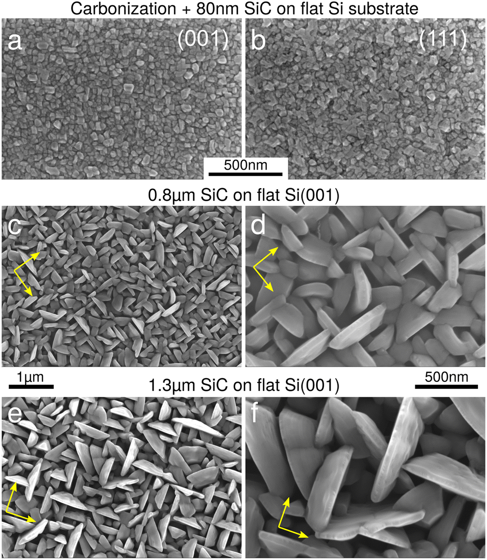 | ||
| Fig. 1 3C-SiC deposition on a flat Si substrate. (a and b) First 80 nm of deposition including the carbonization step and the SiC buffer layer on a flat Si(001) substrate (panel a) and on a flat Si(111) substrate (panel b). (c and d) Deposition of 0.8 μm on a flat Si(001) substrate. (e and f) Deposition of 1.3 μm on a flat Si(001) substrate. SEM images in panels (c)–(f) are acquired at the same magnification for a direct comparison between the size and shape of the platelets. The yellow arrows indicate the 〈110〉 directions. | ||
In order to investigate the progression of the dendritic growth at later stages, after the deposition of several μm of 3C-SiC, we opted for the deposition, under the same growth conditions, on micrometric pillar-patterned Si substrates,13,17 which enables the growth of tens of μm of 3C-SiC by efficiently relaxing the thermal strain.18 This also makes it possible to inspect the platelet morphology by lateral SEM imaging, by cleaving the crystal in between rows of separated pillars. In Fig. 2(a–d) we see approximately 5 μm 3C-SiC deposition on Si(001) at C/Si = 2.6, where the lateral size of the platelets evolved to some μm, whereas the thickness remained of the order of 200 nm. As in the cases shown in Fig. 1, a clear square pattern is constructed by the large majority of the platelets oriented along the four slanted {111} planes while only a few are misaligned at angles of about 30° and 60°. As shown by the lateral view (panel d) some disordered growth occurs at the pillar edges, possibly due to irregularities produced by the Bosch etching process, and some platelets even appear to be vertically oriented.
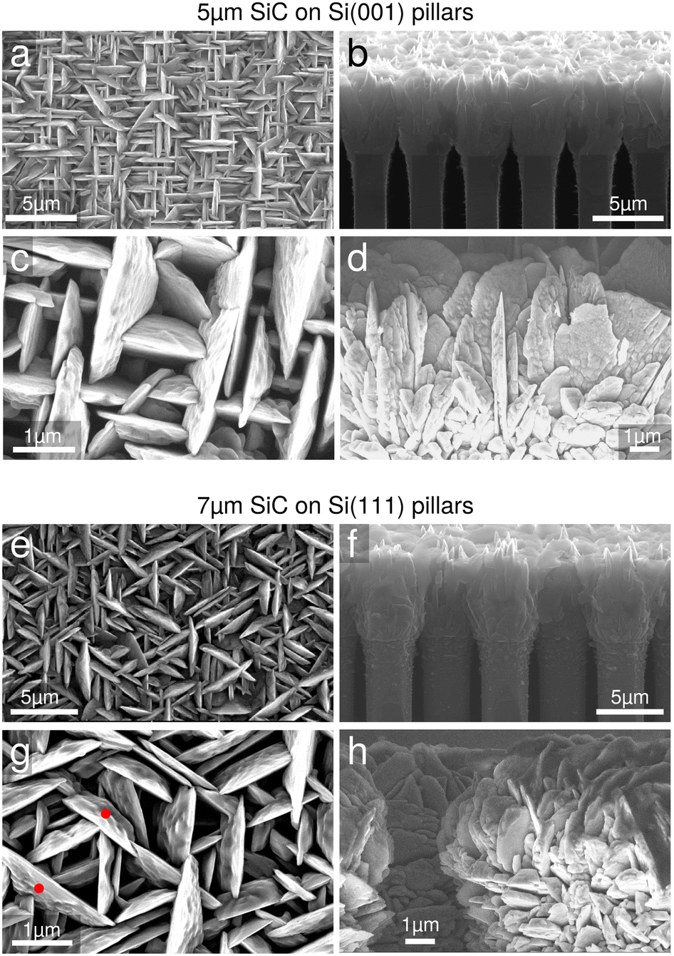 | ||
| Fig. 2 3C-SiC deposition on Si pillars. (a–d) 5 μm SiC on Si(001) substrate and (e–h) 7 μm SiC on Si(111) substrate. Panels (a, c, e, g) top views; panels (b, d, f, h): side views. Panel (c) is at the same magnification level of Fig. 1(c and e) for direct comparison. | ||
The same dendritic growth mode so far reported for a (001) substrate is also obtained in the case of a (111)-oriented Si substrate, as made clear in Fig. 2(e–h) for the deposition of approximately 7 μm 3C-SiC on micro-pillars, with C/Si = 2.2. In this case, a triangular texturing is evident, with platelets extending parallel to the three emerging {111} planes, with an average thickness even smaller than 200 nm. It can also be noticed that some of the platelets appear to have opposite inclination, for example the two platelets marked by red dots in Fig. 2(g), which can again be explained by admitting twinned regions.
By comparing the morphology of the thicker layers of Fig. 2 with the earliest stages of Fig. 1, it can be seen that the texturing in platelets aligned with the (111) planes, with a large aspect ratio between lateral (vertical) dimensions and the thickness, increases as deposition progresses, resulting in a nanostructured film with a high surface-to-volume ratio. In particular, by comparing the top views of Fig. 1(c), (e) and 2(c), reported on the same scale, it is evident that a dramatic selection process occurs during the growth. While at the beginning a large number of small platelets start to grow, at the latest stages only a few large platelets survive, indicating a strong competition with each other. Additional samples were grown at the same temperature (1250 °C) and different C/Si ratios (2.2 and 2.6), as well as at the same C/Si ratio (2.6) and different temperatures (1250 °C and 1300 °C). Both variations are within the parameter range compatible with proper epitaxy. In all cases, the same dendritic growth mode and platelet morphologies were observed (see the comparison in the ESI†), indicating that the mechanism giving rise to this effect is quite robust, when the C/Si ratio is strongly increased and the temperature moderately decreased, with respect to the usual growth conditions.
Structural analysis
The crystal structure and defectivity of the single platelets were inspected by TEM imaging. The samples were prepared via the following procedure: the surface of the grown wafers was lightly scratched with a diamond tip and then flushed with a continuous ethanol stream, in such a way that the platelets detach from the silicon substrate and become dispersed in ethanol. The solution is then transferred into a vial and subjected to gentle sonication in a sonic bath for a few minutes. About 15 μL of the solution from the top portion of the vial was then dropcast onto a TEM Cu grid covered with a thin (3–4 nm) amorphous carbon membrane. TEM imaging was performed at the Microscopy Platform of the University of Milano-Bicocca using a JEOL JEM 2100P operating at 200 kV, equipped with a LaB6 source, and exhibiting a nominal point resolution of 2.4 Å. Real space images and diffraction patterns were then recorded with a Gatan RIO CMOS camera. Images were taken at different magnifications, with the TEM operated in the bright-field (BF) parallel imaging mode and adopting an in-gap objective aperture to maximize contrast.Fig. 3(a) and (b) show the BF-TEM image of a thick 10 μm long SiC platelet grown on a Si(111) substrate and its selected-area diffraction pattern, respectively. The regular hexagonal Bragg peak distribution in the diffraction pattern is indicative of a (111) basal plane. This holds true also for thinner and smaller platelets grown both on a Si(111) substrate (see Fig. 3(e) and (f)) and on a Si(001) substrate (see Fig. 4(a) and (b)).
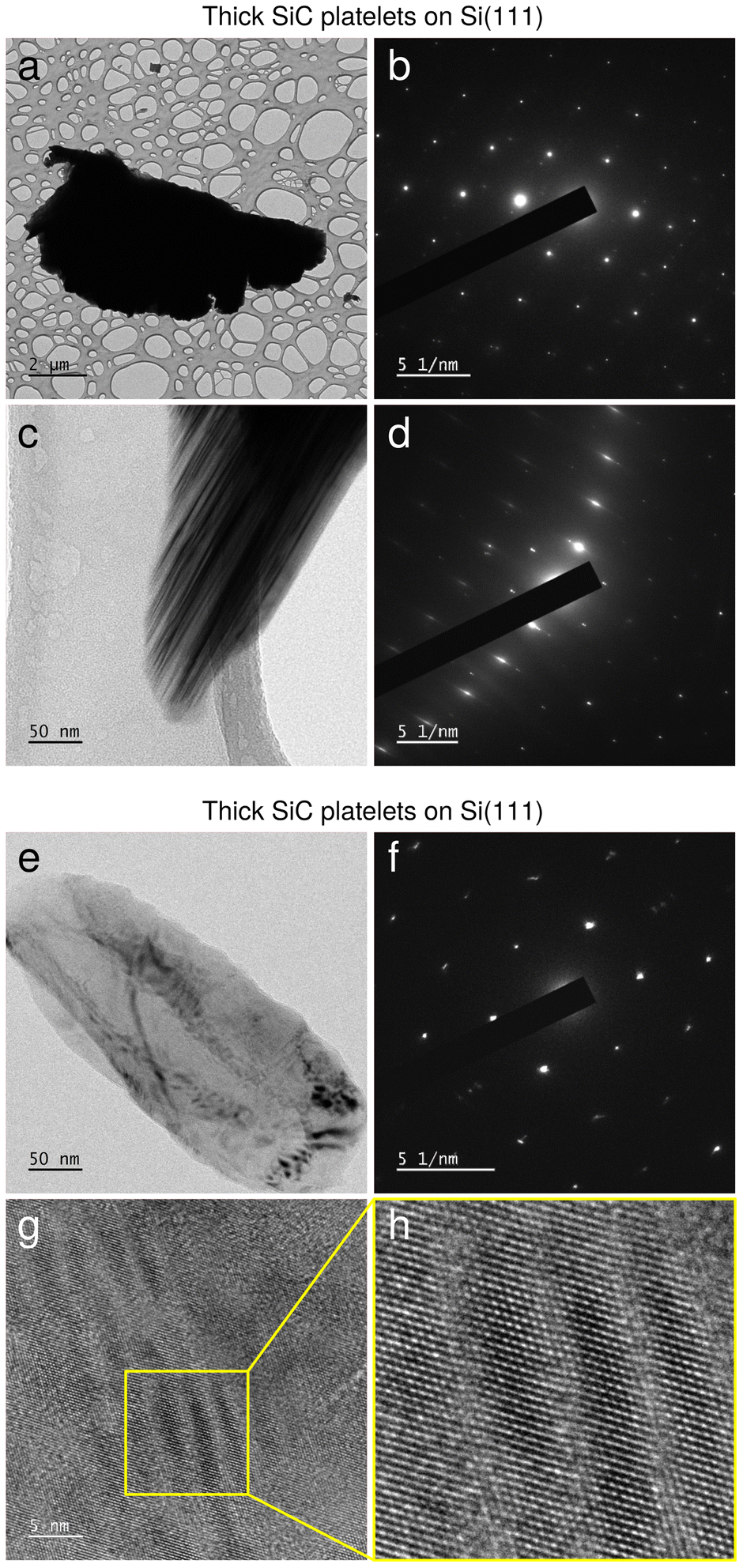 | ||
| Fig. 3 TEM analysis of thick and thin SiC platelets on Si(111). (a) Bright-field TEM image of a thick SiC platelet on Si(111). (b) Diffraction pattern of the platelet shown in panel (a). (c) Bright-field TEM image of a small portion of the thick SiC platelet shown in panel (a) with the sample tilted at about 25° with respect to the (111) basal plane. (d) Diffraction pattern of the platelet portion shown in panel (c). (e) Bright-field TEM image of a thin SiC platelet on Si(111). (f) Diffraction pattern of the platelet shown in panel (e). (g) High-resolution (HR) TEM image of a portion of the thin SiC platelet shown in panel (e). (h) High-magnification portion of the HR-TEM image shown in panel (g). | ||
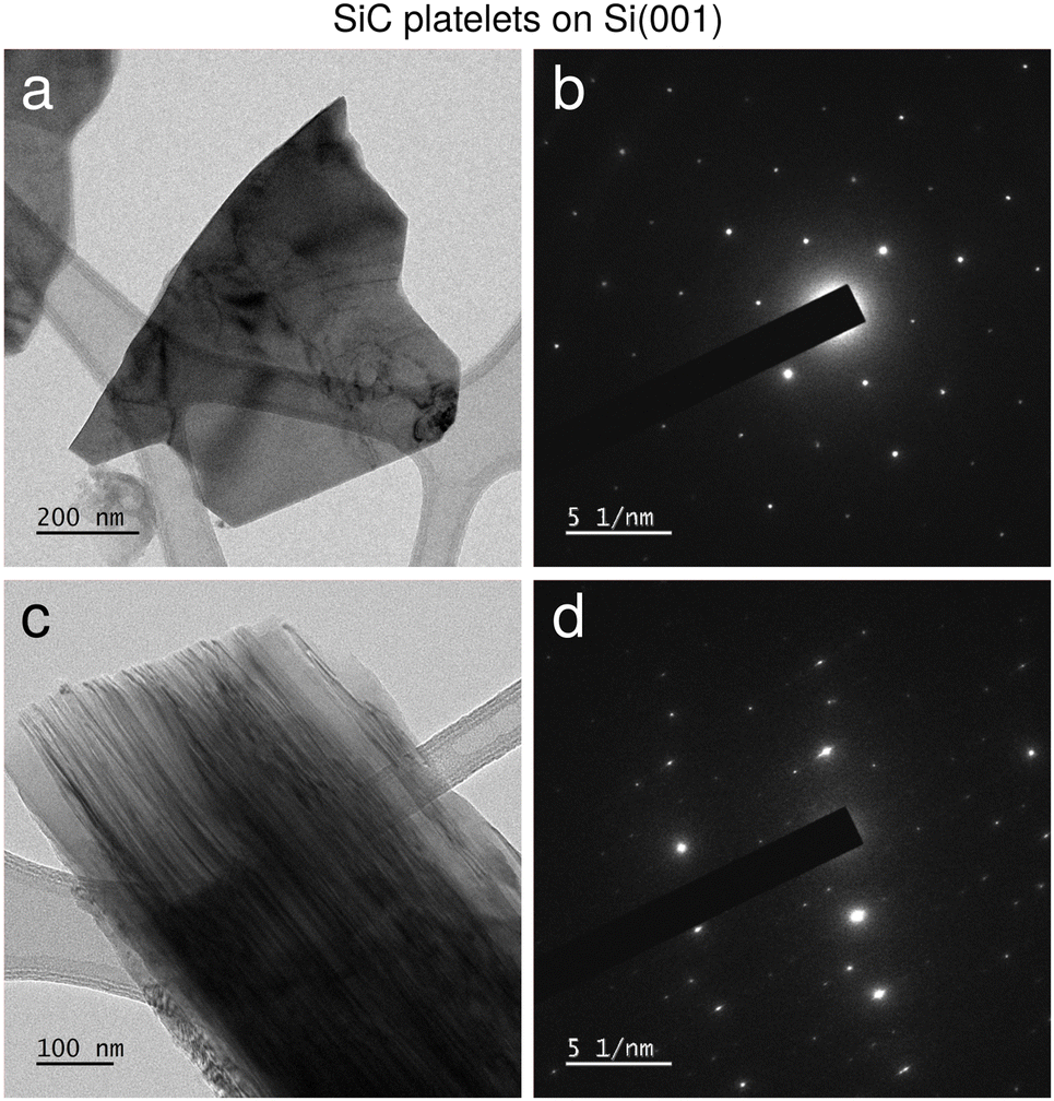 | ||
| Fig. 4 TEM analysis of thick and thin SiC platelets on Si(001). (a) Bright-field TEM image of a thin SiC platelet on Si(001). (b) Diffraction pattern of the platelet shown in panel a. (c) Bright-field TEM image of a thick SiC platelet on Si(001) with the sample tilted at about 10° with respect to the (111) basal plane. (d) Diffraction pattern of the platelet portion shown in panel (c). | ||
More interestingly, TEM analysis of the thick platelets at low magnification and with the sample tilted with respect to the basal plane reveals the presence of a number of straight dark lines corresponding to the projection of stacking faults on the (111) plane.19 These are equally visible in the BF images of thick platelets grown on both Si(111) substrates (Fig. 3(c) and (d)) and on Si(001) substrates (Fig. 4(c) and (d)), revealing a stacking fault density in the order of 2 × 106 cm−1, i.e. 2 SFs every 10 nm. This corresponds to the density commonly seen at the very initial stages (tens of nm) of SiC film growth,20 indicating that there is no mutual annihilation mechanism of differently oriented SFs active within the platelets, for simple aspect ratio reasons. Finally, in Fig. 3(g) and (h) we show High-Resolution (HR) TEM images of the thin platelet reported in Fig. 3(e). The strong interferometric contrast visible in Fig. 3(h) is most likely due to an interference effect caused by an in-plane displacement of the atomic columns lying in the atomic planes below the top one, creating a Moiré pattern with an effective periodicity of about 2.5 nm. This is consistent with the presence of stacking faults in the (111) basal plane.
XRD measurements were performed with a PANalytical X’Pert PRO MRD diffractometer on a large area (several square millimetres) of the samples to assess the overall degree of crystallinity and the epitaxial relationship of the platelets with the substrate. The Cu Kα1 line was used with a wavelength λ = 1.540562 Å, selected by a hybrid 2-bounce monochromator and mirror. The sample was mounted on a Euler cradle, such that measurements were referenced to precise alignment with the (004) or (333) substrate Bragg peak (respectively for (001) or (111) substrates). Diffracted intensity was detected with a Xe proportional detector directly in the beam path such that roughly 1° of 2θ was accepted on either side of the nominal position. In Fig. 5(a), we report symmetric 2θ–ω scans for one sample with (001) substrate orientation and two samples with (111) substrate orientation. For samples grown on Si(001), the SiC(002) and the SiC(004) peaks are observed, while for samples grown on Si(111), the SiC(111), SiC(222) and the SiC(333) peaks are present, since these are the lattice planes which are parallel to the reference substrate planes.
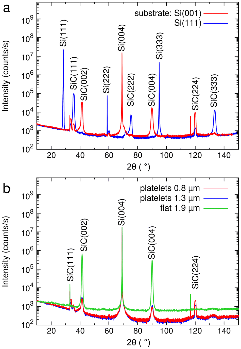 | ||
| Fig. 5 Wide-range 2θ–ω scans, taken with a wide detector acceptance angle in a symmetric diffraction configuration. The scans were aligned on either the Si(004) or the Si(333) substrate peaks for samples grown on (001) and (111) Si substrates. (a) Comparison of scans for samples grown on pillar-patterned substrates on both (100) and (111) Si substrates under similar conditions to those in Fig. 2. (b) Comparison of the scans obtained for samples grown on planar (001) Si substrates, both in the cases of Fig. 1 with platelet growth and for a flat-layer growth with conventional parameters. | ||
However, an additional peak attributed to SiC(224) appears at 2θ ≈ 120° for both substrate orientations. Given the symmetric configuration of the XRD measurement, such a peak indicates that some SiC(224) planes do align parallel to the (001) or (111) substrate plane. This is not compatible with the crystallography of a (001)- or (111)-oriented 3C-SiC perfect crystal but could be the consequence of the presence of structural defects (e.g., multiple twins), locally changing the lattice orientation. This could be the case for the vertically oriented platelets recognizable in some lateral SEM views (see e.g., Fig. 2(d)). We investigated this last finding more deeply by comparing the 2θ–ω scan of the two samples with platelets from Fig. 1(c–f) and the 2θ–ω scan of a flat 3C-SiC film on Si(001) grown under the typical conditions of a low C/Si ratio (here ≈ 0.7) and a high temperature (1370 °C). Results are reported in Fig. 5(b). As evident, an anomalous (224) peak is observed for both samples with platelets but not for the flat growth (and indeed has never been reported in the literature to the best of our knowledge). Therefore, we can infer that the finite dimensions of the sheets and the particular conditions responsible for the dendritic growth mode allow monocrystalline platelets to nucleate at specific degrees of misorientation with respect to the substrate. This mechanism is not affected by substrate patterning, since the same result is seen for growth both on pillars (Fig. 5(a)) and on planar substrates Fig. 5(b).
Discussion and structural model
In the experimental analysis discussed in the previous section we have shown how the particular low-temperature and high C/Si ratio growth conditions used here result in a highly textured growth mode. Such conditions are expected to quench the surface diffusion and the nucleation of 2D islands, giving rise to a large roughness, as reported in the literature,10,21,22 while still preserving the possibility of a crystalline growth. This makes the formation of overcritical islands on close-packed singular surfaces, such as the (111) and (001), very difficult, so that the usual crystalline incorporation mechanism is essentially inhibited. More in detail, due to the carbonization process, the (111) and the (001) basal surfaces are Si-terminated. Most of the Si dangling bonds are expected to be fully saturated by carbon radicals because of the high C/Si ratio. Then, the reactive incorporation of TCS in overcritical islands is likely to be prevented for kinetic reasons, despite considering the same optimal flux of the typical high-temperature planar growth. The only way to proceed with crystalline growth would be to have a more open structure at the growth front, possibly exhibiting both Si and C sites, so that the reactive incorporation of SiC units is enhanced, despite the reduced surface diffusion. Actually, Lateral Epitaxial Overgrowth (LEO) of 3C-SiC on silicon dioxide patches, by selective deposition of hexachlorodisilane and propane, as well as hexamethyldisilane, on Si(001) at reduced temperature23 demonstrated that the {112} surfaces, as well as minor {117} surfaces, behave as fast-growing lateral growth fronts. Indeed, the {112} facet, shown in Fig. 6(a), is both open in structure and non-polar, as are other {11n} facets. Moreover, in ref. 21 the {112} surface was reported to be, together with the {110} facet, a better growth front for 3C-SiC incorporation with silane and propane, even at a higher C/Si ratio, to overcome anti phase domains on (001) substrates. Still, in that paper the authors showed that it is not possible to use (112) oriented wafers for a good crystalline epitaxy, as the carbonization process (producing one full initial carbon layer) is inconsistent with the presence of both Si and C sites in the same growth front. Therefore, it appears that the need to start with (001) and (111) Si wafers excludes those growth-front orientations that could justify a fast vertical growth in the present regime of a reduced temperature and a high C/Si ratio.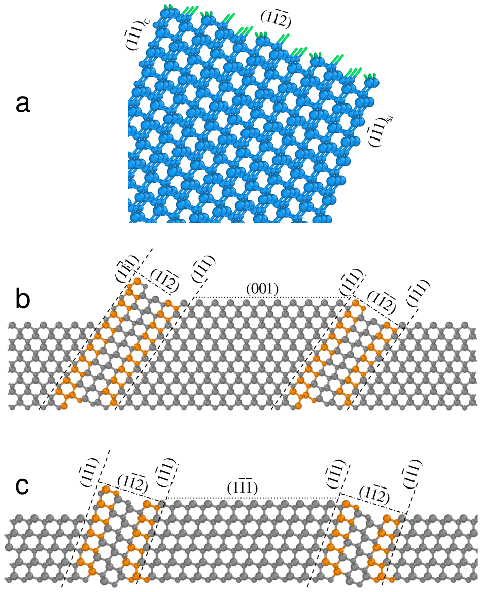 | ||
| Fig. 6 Atomistic model of the growing structure and the appearance of the 〈112〉 growth front at the emergence of SFs. (a) Atomic structure of the {112} facet as bounded by perpendicular {111} planes. Reconstruction of the structure of the growth front of a platelet on the (001) (b) and (111) (c) surfaces. | ||
However, here the SFs come in, not only as a problem in power device manufacturing, but also as a crystallographic alternative to the problem above. Ref. 24 explains the growth of relatively long lathlike dendrites of germanium from undercooled melts and argues that the presence of at least two twinning planes on {111} facets may result in two {112} striped free facets with a concave corner, returning a fast growth front, while the more closed {111} sidewalls extend indefinitely in two dimensions. The paper also suggested that a series of steps and kinks in such a growth front, while still preserving a series of {112} facets, may result in a macroscopically curved boundary, similarly to the platelet edges in our experiments (see e.g.Fig. 4(c)).
The platelets considered in this work consist of {111} sheets with multiple SFs parallel to the exposed faces emerging at the thin side and top rims, i.e., at the fast growth fronts. In Fig. 6(b) and (c) we show the atomistic structure of such rims including a couple of triple SFs emerging on the (001) and (111) surfaces, respectively, with {112} striped facets, elongating perpendicular to the figure in the 〈110〉 directions. These {112} nanofacets not only represent an open growth front with Si and C sites, but also constitute a series of emerging slanted steps that allow for the easier incorporation at the (111) or (001) portions in between two steps (as indicated in Fig. 6), by an active step-flow mechanism, even at the reduced surface diffusion length (still presumed to be larger than some ten nm). Then, we conclude that the emergence of SFs at the rims of the growing platelets is the trigger for the enhanced anisotropy in the growth velocity within a single wafer orientation, either (001) or (111). The emerging {111} facets remain the slowest in growing, and the {112} facets of the SFs make the platelet growth front the fastest. Notably, since the SF planes are perpendicular to such {112} fronts, this mechanism is self-sustained thus driving the extension of the platelets during the growth. Reasonably, the fastest growth is found in the vertical direction, where the flux supply is maximum, while the lateral expansion of the {111} side facets, still extending in width up to a few microns, can be limited by mutual flux shielding effects and collision between nearby platelets.
The reason why our platelets grow with a thickness of several tens to few hundred nm, as spaced by some hundred nm on the average, despite the average spacing in the SFs is estimated to be of the order of 10 nm, may be traced back as follows. The growth starts just after the buffer layer deposition from grains below 100 nm in size (see Fig. 1(a and b)), exposing different facets; most of them contain SFs in bunches which provide a fast growth front. More precisely, in the grain SFs could be present with all possible orientations of {111} planes, i.e., along four directions on (001) substrates and three on (111) substrates. While all these orientations could lead to growth enhancement, statistically, there will be just one which prevails, thus selecting the platelet orientation. SFs aligned in all other orientations will then propagate only in the bottom of the 2D structure and be expelled through the established {111} lateral faces.
At the initial stages, some competition with different grains is still present (see Fig. 1(c and d)). As the deposition proceeds, the platelets which originate from the better oriented grains (still predominantly monocrystalline) take over (see Fig. 1(e and f)) and a progressive focusing of the growth along the SF bunches occurs, showing a square or a triangular pattern, on the (001) and (111) wafers, respectively (Fig. 2(a and e)). Such a symmetrical arrangement fully matches the symmetry of the {111} planes on the growth substrate, i.e., of the SFs driving the dendritic growth. This intimate connection between the platelets and the {111}-SF planes can be assumed to hold also in the case of some misaligned platelets, thus giving a fingerprint of local lattice misorientations. In particular, SEM top views indicate a prevalence of misaligned platelets at about 30° and 60° with respect to 〈110〉 directions on the (001) substrate while on the (111) substrate platelets are observed with mirror-inclination (i.e., rotated by 180°). The latter case can be immediately understood by considering a local twinning in the (111) basal plane, an occurrence that is quite commonly reported in the literature.4,25,26 This twinning process should be already present from the very beginning of the growth, i.e., in the grains of Fig. 1(b), as the SF emerge; it is likely that the 3D nature of the grains facilitates such a process. Similarly, for the (001) substrate, twinning in one of the four {111} slanted planes generates a rotation in the SF-planes explaining the observed misorientation of the platelets. In ref. 27 it was shown by electron back scattering diffraction and HR-TEM analyses that (111) grains with (111) orientation can be produced at the edges of 3C-SiC microcrystals grown on Si(001) pillars, even under the optimal growth conditions for a planar film. This process requires a double twinning delimiting the grain in the crystalline matrix, and it is very likely that this happens also in the 3D grains in our case. An atomistic reconstruction of regular and misaligned platelet structure is reported in the ESI.† The reason why the width of the platelets increases from tens to a few hundred nm can be understood by considering the nucleation of more SFs on the slowly growing (111) sidewalls, probably originating at the basal plane. A curved and jagged profile perpendicular to the [111] direction of the platelets, appearing in Fig. 2(d) and (h) for the two substrate orientations, is seen as the result of steps connecting the different {112} growth fronts (vertical and lateral), producing the whole lateral expansion starting from the initial grains. Finally, the best growth conditions for (001) and (111) flat films, 1370 °C and a Si/C ratio below 1, are understood in terms of larger surface diffusion length and the larger nucleation probability of two-dimensional overcritical Si islands on such singular surfaces which cancels the competitive advantage of {112} striped facets.
Despite that the mechanism so far described fully relies on kinetics, it is worthwhile to discuss if any thermodynamic contribution is present. For films as thick as some 5–7 μm, the formation of SF bunches constituting the platelets certainly leads to an enormous increase in the surface for both Si(001) and Si(111). Thus, a corresponding increase in surface energy, independent of any surface reconstruction at the growth temperature, is envisaged. Since the platelets with SF bunches are laterally decorated by regular 3C-SiC(111) layers, the increase in surface energy would be not very different for a platelet without any SFs. Hence, concerning the surface energy change, the SF bunches constituting the platelets are equivalent to platelets without SFs and both of them clearly increase the surface energy with respect to a flat 3C-SiC layer. Concerning the volume contributions, one may expect that the formation of a platelet with SFs does not have a different volumetric energy with respect to the 3C-SiC crystal structure. In fact, only some minor strain is introduced by SFs in the bulk, but the large free surfaces of the nanometric platelet should accommodate the corresponding stress. Thus, considering the very low formation energy of SFs in 3C-SiC,7 the bulk contribution to the formation energy of the platelets is almost null, regardless of whether SF bunches are included. This is confirmed by classical molecular dynamics simulations reported in the ESI,† comparing the energy for each additional layer on the growth front of an unfaulted ridge with that of a ridge formed by a triple SF, for both (001) and (111) substrate orientations. The results indicate that the energy change for any additional layer is the same for the two cases, except for the initial stages of emergence of the SF, where the latter is favoured until the first monoatomic (slanted) step is created. This means that a bunch of monoatomic steps emerges from the very beginning of the growth, independent of any kinetic issue, in turn favouring the step-flow growth of the basal plane in between the SFs right from the initial stages of the growth on the grains. After the initial stages, the formation of SF bunches is favoured kinetically rather than thermodynamically.
Conclusions
In conclusion, we have demonstrated that the (111) oriented 3C-SiC nanoplatelets containing bunches of SFs can be grown by usual thermal CVD, thanks to their intrinsic structural features, which strongly enhance the growth kinetics. In this method, micron-thick textured 3C-SiC films with a high surface-to-volume ratio can be deposited on Si(001) and Si(111) substrates using an industrial reactor under suitable, but sufficiently robust, kinetic growth conditions. Due to the extremely large (111) exposed surface and to the monocrystalline nature of the films, interesting applications can be envisaged, not only in integrated thermal sinks and water-splitting photocathodes, but also in sensors and natural adhesive layers for power device bonding in ICs. In addition to the promising applications of such films, a more fundamental understanding of the 3C-SiC microstructure is revealed by our work; the 3D nature of the initial grains, and the isolation of SF bunches allowed by their 2D free expansion within the platelets provide a fingerprint of the twinning processes which easily occur in this material.Author contributions
Investigation and data curation: G. M. V., D. Ch., A. B., M. M., and G. C.; methodology and formal analysis: E. S., L. B., A. M., and R. B.; supervision: F. L. V., D. Cr., and L. M.; conceptualization: A. M., R. B., and L.M.; writing – original draft: G. M. V., D. Ch., A. M., R. B., and L. M.; writing – review & editing: E. S., L. B., A. B., M. M., F. L. V., G. C., and D. Cr.; resources: D. Cr.Conflicts of interest
There are no conflicts to declare.Acknowledgements
Authors acknowledge EU for funding the CHALLENGE project (3C-SiC Hetero-epitaxially grown on silicon compliance substrates and 3C-SiC substrates for sustainable wide-band-Gap power devices) within the EU's H2020 framework program for research and innovation under grant agreement no. 720827.References
- F. La Via, M. Zimbone, C. Bongiorno, A. La Magna, G. Fisicaro, I. Deretzis, V. Scuderi, C. Calabretta, F. Giannazzo, M. Zielinski, R. Anzalone, M. Mauceri, D. Crippa, E. Scalise, A. Marzegalli, A. Sarikov, L. Miglio, V. Jokubavicius, M. Syväjärvi, R. Yakimova, P. Schuh, M. Schöler, M. Kollmuss and P. Wellmann, Materials, 2021, 14, 5348 CrossRef PubMed.
- A. B. Renz, F. Li, O. J. Vavasour, P. M. Gammon, T. Dai, G. W. C. Baker, F. La Via, M. Zielinski, L. Zhang, N. E. Grant, J. D. Murphy, P. A. Mawby, M. Jennings and V. A. Shah, Semicond. Sci. Technol., 2021, 36, 055006 CrossRef CAS.
- P. Schuh, F. La Via, M. Mauceri, M. Zielinski and P. J. Wellmann, Materials, 2019, 12, 2179 CrossRef CAS.
- M. Agati, S. Boninelli, C. Calabretta, F. Mancarella, M. Mauceri, D. Crippa, M. Albani, R. Bergamaschini, L. Miglio and F. La Via, Mater. Des., 2021, 208, 109833 CrossRef CAS.
- E. Scalise, L. Barbisan, A. Sarikov, F. Montalenti, L. Miglio and A. Marzegalli, J. Mater. Chem. C, 2020, 8, 8380–8392 RSC.
- F. Li, F. Roccaforte, G. Greco, P. Fiorenza, F. La Via, A. Pérez-Tomas, J. E. Evans, C. A. Fisher, F. A. Monaghan, P. A. Mawby and M. Jennings, Materials, 2021, 14, 5831 CrossRef CAS PubMed.
- F. Giannazzo, G. Greco, S. Di Franco, P. Fiorenza, I. Deretzis, A. La Magna, C. Bongiorno, M. Zimbone, F. La Via, M. Zielinski and F. Roccaforte, Adv. Electron. Mater., 2020, 6, 1901171 CrossRef CAS.
- E. Scalise, A. Marzegalli, F. Montalenti and L. Miglio, Phys. Rev. Appl., 2019, 12, 021002 CrossRef CAS.
- A. Veneroni, F. Omarini, D. Moscatelli, M. Masi, S. Leone, M. Mauceri, G. Pistone and G. Abbondanza, J. Cryst. Growth, 2005, 275, e295–e300 CrossRef CAS.
- M. Masi, A. Veneroni, A. Fiorucci, F. La Via, G. Foti, M. Mauceri, S. Leone, G. Pistone, G. Condorelli, G. Abbondanza, G. L. Valente and D. Crippa, Mater. Sci. Forum, 2007, 556–557, 93–96 CAS.
- J. Jian and J. Sun, Sol. RRL, 2020, 4, 2000111 CrossRef CAS.
- X. Han, S. Heuser, X. Tong, N. Yang, X. Guo and X. Jiang, Chem. – Eur. J., 2020, 26, 3586–3590 CrossRef CAS PubMed.
- M. Masullo, R. Bergamaschini, M. Albani, T. Kreiliger, M. Mauceri, D. Crippa, F. La Via, F. Montalenti, H. von Känel and L. Miglio, Materials, 2019, 12, 3223 CrossRef CAS.
- J.-J. Huang, C. Militzer, C. Wijayawardhana, U. Forsberg, L. Ojamäe and H. Pedersen, J. Phys. Chem. C, 2022, 126, 9918–9925 CrossRef CAS.
- H. Zhuang, L. Zhang, R. Fuchs, T. Staedler and X. Jiang, Sci. Rep., 2013, 3, 2427 CrossRef PubMed.
- C. Wang, N. Huang, H. Zhuang, Z. Zhai, B. Yang, L. Liu and X. Jiang, Surf. Coat. Technol., 2016, 299, 96–103 CrossRef CAS.
- H. von Känel, F. Isa, C. V. Falub, E. J. Barthazy, E. Müller Gubler, D. Chrastina, G. Isella, T. Kreiliger, A. G. Taboada, M. Meduna, R. Kaufmann, A. Neels, A. Dommann, P. Niedermann, F. Mancarella, M. Mauceri, M. Puglisi, D. Crippa, F. La Via, R. Anzalone, N. Piluso, R. Bergamaschini, A. Marzegalli and L. Miglio, ECS Meet. Abstr., 2014, MA2014-02, 1822 CrossRef.
- M. Albani, A. Marzegalli, R. Bergamaschini, M. Mauceri, D. Crippa, F. La Via, H. von Känel and L. Miglio, J. Appl. Phys., 2018, 123, 185703 CrossRef.
- G. Agrosì, G. C. Capitani, E. Scandale and G. Tempesta, Phys. Chem. Miner., 2011, 38, 101–109 CrossRef.
- C. Wen, Y. M. Wang, W. Wan, F. H. Li, J. W. Liang and J. Zou, J. Appl. Phys., 2009, 106, 073522 CrossRef.
- K. Shibahara, S. Nishino and H. Matsunami, J. Cryst. Growth, 1986, 78, 538–544 CrossRef CAS.
- C. H. Wu, C. Jacob, X. J. Ning, S. Nishino and P. Pirouz, J. Cryst. Growth, 1996, 158, 480–490 CrossRef CAS.
- A. R. Bushroa, C. Jacob, H. Saijo and S. Nishino, J. Cryst. Growth, 2004, 271, 200–206 CrossRef CAS.
- D. R. Hamilton and R. G. Seidensticker, J. Appl. Phys., 1960, 31, 1165–1168 CrossRef CAS.
- C. Long, S. A. Ustin and W. Ho, J. Appl. Phys., 1999, 86, 2509–2515 CrossRef CAS.
- A. Severino, C. Bongiorno, N. Piluso, M. Italia, M. Camarda, M. Mauceri, G. Condorelli, M. A. Di Stefano, B. Cafra, A. La Magna and F. La Via, Thin Solid Films, 2010, 518, S165–S169 CrossRef CAS.
- M. Meduňa, T. Kreiliger, I. Prieto, M. Mauceri, M. Puglisi, F. Mancarella, F. La Via, D. Crippa, L. Miglio and H. von Känel, Mater. Sci. Forum, 2016, 858, 147–150 Search PubMed.
Footnotes |
| † Electronic supplementary information (ESI) available: Additional samples at different temperatures and C/Si ratios; molecular dynamics model and calculations; structural analysis of the platelet symmetry and role of twinning. See DOI: https://doi.org/10.1039/d2cp03250c |
| ‡ G. M. Vanacore, D. Chrastina and R. Bergamaschini contributed equally to this work. |
| This journal is © the Owner Societies 2022 |