
 Open Access Article
 This Open Access Article is licensed under a
 Creative Commons Attribution 3.0 Unported Licence
Electron-hopping across dye-sensitized mesoporous NiO surfaces†
Sina
Wrede
 a,
Lanlan
He
b,
Gerrit
Boschloo
a,
Leif
Hammarström
a,
Lars
Kloo
*b and
Haining
Tian
*a
a,
Lanlan
He
b,
Gerrit
Boschloo
a,
Leif
Hammarström
a,
Lars
Kloo
*b and
Haining
Tian
*a
aDepartment of Chemistry-Ångström Laboratory, Uppsala University, SE-75120 Uppsala, Sweden. E-mail: haining.tian@kemi.uu.se
bDivision of Applied Physical Chemistry, Centre of Molecular Devices, Department of Chemistry, KTH Royal Institute of Technology, SE-10044 Stockholm, Sweden. E-mail: larsa@kth.se
First published on 23rd November 2022
Abstract
To gain a deeper understanding of the underlying charge processes in dye sensitized photocathodes, lateral electron hopping across dye-sensitized NiO photocathodes was investigated. For dye-sensitized systems, hole hopping across photoanodes has been studied extensively in the literature but no expansive studies on electron hopping in sensitized photocathodes exist today. Therefore, an organic p-type dye (TIP) with donor–linker–acceptor design, showing high stability and electrochemical reversibility, was used to study the electron transfer dynamics (electron-hopping) between dyes with temperature dependent spectroelectrochemistry and computational simulations. Besides intermolecular electron-hopping across the surface with a rate constant in the order of 105 s−1, our results show a second electron hopping pathway between NiO surface states with a rate constant in the order of 107 s−1, which precedes the electron hopping between the dyes. Upon application of a potential step negative enough to reduce both the dye and NiO surface states, the majority of NiO surface states need to be reduced before intermolecular electron transfer can take place. The results indicate that, in contrast to sensitized photoanodes where intermolecular charge transfer is known to influence recombination kinetics, intermolecular charge transport processes in TIP dye sensitized NiO photocathodes is less relevant because the fast electron transport between NiO surface states likely dominates recombination kinetics.
Introduction
In the wake of global warming, which impacts not only the climate1,2 but also aggravates global inequality,3,4 the sun has been identified as one of the most promising alternative energy providers to fossil fuels. To exploit its vast availability, the sun's photons first need to be transformed into energy-rich charge carriers which can either be used directly as electricity or stored in the form of a chemical bond, a so-called solar fuel or other chemicals.One approach for solar energy conversion and storage is dye-sensitized solar cells (DSC) or dye-sensitized photoelectrochemical cells (DS-PEC) which are utilizing molecular photosensitizers (dyes) in combination with mesoporous wide band-gap semiconductors. The photosensitizers are anchored on the semiconductor surface5 and in the case of DS-PECs, catalysts for a desired reaction (e.g. water splitting) can be additionally introduced.6,7 They provide a low-cost strategy that is based on earth abundant materials, especially if organic dyes are used instead of heavy-metal (such as ruthenium) containing photosensitizers, making their resource limitations less critical than for other solar conversion technologies.8,9 As solar conversion efficiencies still remain challenging, especially for p-type (photocathode) devices, understanding the underlying charge transfer processes, such as electron transfer, is not only a question of scientific curiosity but a necessity for developing more efficient devices in the future.
In the conventional understanding of such devices, the excited dye injects a charge into the semiconductor before the corresponding redox equivalent remaining on the dye is (i) regenerated by the electrolyte, generating an electric current or (ii) transferred to the catalyst, driving the reaction for solar fuel production.10,11 However, if there is a strong electronic coupling between the molecular photosensitizers, lateral charge hopping across the semiconductor surface can take place.12 This hopping process has been studied extensively for photoanodes with TiO2 as mesoporous metal oxide film, both direct dye-to-dye hopping as described by Marcus theory13,14 and with diffusional mediatiors.15–17 For photoanodes, the photosensitizer injects an electron into the n-type semiconductor, leaving a hole behind which can undergo lateral intermolecular charge transfer. This hole hopping process has been studied for various dyes, both with electrochemical13,14 and photo-induced18–20 hole transfer, and revealed that hole hopping can be both advantageous and deleterious. For example, it can be exploited in a more unconventional electrolyte-free DSC to transfer redox equivalents across a sensitized electrode, leading to charge transport between the two electrodes in the device.21 Furthermore, lateral hole transfer has been shown to aid in the accumulation of charge carriers on a single catalytic site which is necessary for many reactions, such as water oxidation.18,22 At the same time, if the charge hopping is fast, studies of dye sensitized TiO2 have revealed that recombination with injected electrons in the semiconductor proceeds more rapidly.23,24 From all of these studies, it can be concluded that intermolecular charge hopping can affect the overall performance of the resulting devices.
In contrast to the n-type analogue, the lateral charge hopping between dyes on photocathodes, for which NiO is typically chosen as p-type semiconductor, has not been investigated as extensively though electron self-exchange has been proposed as a mechanism in H2-evolving photocathodes by Hammarström and coworkers.25,26 Kaeffer et al. observed electrochemically induced lateral catalyst electron transfer for a cobalt-diimine catalyst across a NiO photocathode.27 However, it is still unknown if an electron hopping process between the photosensitizer could exist alongside other charge transfer processes at the interface, such as charge recombination between the reduced dye and the p-type semiconductor or the regeneration of the dye by the redox couple in the electrolyte. Furthermore, NiO has been shown to have a more complex nature than TiO2: NiO exhibits a much higher density of trap states and complex electronic states. These so called “surface states” are complex in nature and not fully understood and this work does not aim to solve the nature of these states but instead investigate the electron hopping processes in NiO photocathodes. Though the two redox signatures visible in cyclic voltammetry that have been assigned to these states have been studied with XPS in vacuum in the past and proposed to be Ni3+ and Ni4+ states of various possible higher valence nickel oxide hydroxide and nickel hydroxide species,28 Flynn et al.29 assigned them to be Ni vacancy defect states. D’Amario et al. have proposed at least two different kinds of surface states that act as shallow and deep traps and connected them to higher valence Ni states.30,31
In combination with their complex nature, the presence of these surface states has been shown to have an impact on the sensitized photocathode performance since they can act as recombination centers,32 and are suggested to be involved in the working principle of p-type DSCs and in solar fuel devices for dye regeneration and electrolyte catalysis.33 Therefore, it remains unclear if the surface states of NiO could also have an impact on a possible lateral electron hopping process between the photosensitizers. Understanding these processes could help us to further improve the performance of photocathodes for solar cells and solar fuel devices.
In order to study the intermolecular electron hopping across a dye sensitized photocathode, we used the organic TIP dye34 and mesoporous NiO film, the most popular p-type semiconductor for photocathodes, as a model system (Fig. 1). The TIP dye exhibits the donor–linker–acceptor design, which is a common design strategy to reduce charge recombination through intramolecular charge separation between the donor and acceptor unit, leaving an electron behind on the acceptor unit after hole injection into NiO.35 TIP shows high stability and electrochemical reversibility, as well as high molar extinction coefficient in the visible region, which offers us an ideal model to track optical changes upon electrochemical reduction for this electron hopping study.
 | ||
| Fig. 1 Schematic picture of the investigated system with sensitized NiO, where the reduced dye is depicted in blue, undergoing electron hopping. The organic photosensitizer TIP has a donor–linker–acceptor design. | ||
Method
Lateral electron hopping in a dye-sensitized mesoporous NiO film was studied with spectroelectrochemistry, which has become a well-established method to assess the diffusion of charges across a surface.16,24,36–38 Upon application of a negative potential to reduce the sensitizer, the change in absorption over time of chosen spectral features were monitored. From the extracted kinetic traces, an apparent diffusion coefficient Dapp can be determined from analysis with the Cottrell equation, which typically relates the charge exchanged with an electrode film over time.39,40 However, for electrochromic films, where the change in absorption is proportional to the charge passed, the Cottrell equation can be used to relate the change in absorption ΔA to the apparent diffusion coefficient Dapp throughout the film with a thickness d, where ΔAf is the final or rather maximal possible absorbance change, as it is only valid in the limit of ΔA ≤ ΔAf (eqn (1)).16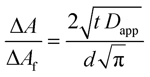 | (1) |
A schematic illustration of the hopping process across the film during spectroelectrochemistry is given in Fig. 2A. A typical visualization of the results from this type of experiment is plotting the measured change in absorption versus the square root of time, in an Anson plot.41,42 The apparent diffusion coefficient in the film, Dapp, can then be extracted from the slope of the initial region, since the mesoporous film has a finite thickness. This is because the equation was derived using semi-infinite diffusion boundary conditions for molecules able to diffuse away from the surface of an electrode.14,16,38 However, for sensitized mesoporous films, the molecules are bound to the thin film with a finite thickness, meaning they do not adhere to this boundary condition and the data deviates from the predicted linear relationship. Therefore, once the frontline of reduced molecules reaches the outer edge of the film, the absorption change becomes time-independent.12 Despite this deviation, it has been shown in the literature that the predicted linear relationship is maintained even for sensitized films for approximately the first 60% of total absorption change.14,16,38
 | ||
| Fig. 2 (A) Schematic illustration of the sensitized NiO film upon application of a potential step during spectroelectrochemistry experiment. (B) Electron self-exchange (hopping) between two dye molecules where the involved acceptor part is highlighted and the reorganization of the solvent and ion distribution is illustrated. (C) Energy diagram for electron self-exchange according to Marcus Theory, where the rate constant depends on the free-energy barrier (ΔG‡) and the electronic coupling (HAB). | ||
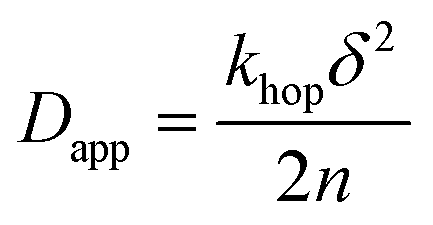
The values of Dapp determined from the slope of the fitted linear region in Anson's plots could then be used to extract the hopping frequency of charges between molecules on the surface. Considering a uniform arrangement of dyes with a constant intermolecular distance δ, Dapp can be expressed with eqn (2), which describes a n-dimensional transport processes43 depending on the intermolecular distance where khop is the first-order self-exchange rate constant, in this study called the hopping rate khop.
 | (2) |
For electron transfer reactions, Marcus theory is well established as a common theory to describe the rate of charge transfer rate constant k between molecules. The general expression for the transfer rate constant is given in eqn (3), where HAB is the electronic coupling between the electron donor and electron acceptor, λ is the reorganization energy and the difference in free energy between the equilibrium states of products and reactants is ΔG°.
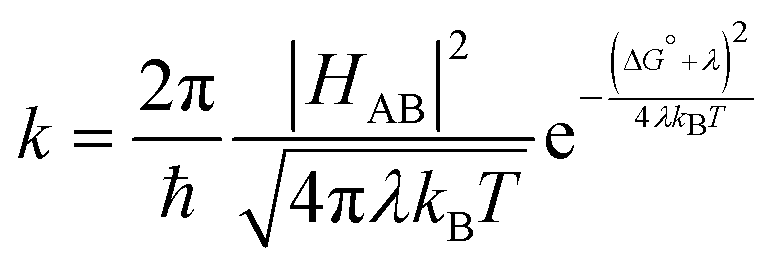 | (3) |
In the case of electron self-exchange, the electron transfer rate describes the hopping between two identical molecules, with ΔG° = 0, simplifying the equation, as shown in eqn (4).
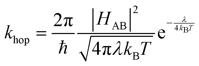 | (4) |
The reorganization energy is the energy required to reorganize the molecular conformation (inner reorganization energy) and the surrounding medium (outer reorganization energy) to their product conformations but without transferring the electron. For a self-exchange, this is just the vertical energy difference between the reactant and product states at the reactant equilibrium reaction coordinate (Fig. 2C). Then the activation free energy ΔG‡ = λ/4, and represents the energy of a compromise nuclear configuration where the reactant and product states are isoenergetic. The reorganization of the solvent during the hopping process is illustrated in Fig. 2B.
In contrast to molecules in solution, that can move freely and are expected to form an “encounter complex”, immobilization of the dyes on the surface restricts molecular motion, which is why nonadiabatic electron transfer (see Fig. 2C) with very weak electronic coupling is assumed for sensitized films, meaning HAB ≪ kBT.12,13 However, it has been hypothesized that adiabatic pathways may be possible upon dye aggregation.44
Through temperature dependent measurements of the charge transfer rate, the reorganization energy associated with electron hopping between the dyes on NiO could be determined by using the Marcus theory to model the data determined experimentally.
Results and discussion
Investigated system
Surface area and properties of the NiO film play a key role in dye-sensitized photocathodes. For this study, NiO films were prepared via screen printing to ensure high reproducibility between films. The film thickness on FTO-glass was determined to be 1.1 μm with an estimated surface area of ABET = 73 m2 cm−3 and an approximate porosity of 40% (see ESI† for further information). The pristine NiO films were sensitized with the donor–linker–acceptor organic dye, TIP, which consists of a triphenylamine donor moiety, indacenodithieno[3,2-b]thiophene (IDTT) linker unit and perylene monoimide (PMI) as acceptor (Fig. 1). The donor–linker–acceptor design, especially with PMI as acceptor and triphenylamine as donor, of the chosen TIP dye is common for p-type organic photosensitizers as the intramolecular charge separation has shown to be beneficial.34,45–47 The ground state absorption of pristine NiO films and sensitized NiO films, abbreviated as NiO and NiO-TIP respectively, immersed in 0.1 M TBAPF6/acetonitrile are shown in Fig. 3. This shows two primary absorption features of the TIP dye at 440 nm and 530 nm. The dye loading determined from de-loading of sensitized films revealed a good surface coverage on the NiO films of 75 μmol cm−3, which corresponds to an average surface area occupied by one TIP molecule of approximately 155 Å2. Therefore, we conclude that the sensitized NiO thin films in this study are typical for those in the literature for organic dye-sensitized photocathodes for solar cells and solar fuels. | ||
| Fig. 3 Steady-state absorption spectrum of NiO and NiO-TIP films immersed in 0.1 M TBAPF6/acetonitrile, a photograph of the two types of films are shown in the inset. | ||
Cyclic voltammetry of the sensitized NiO films showed a half-wave reduction potential of TIP of E1/2 = −1.21 V vs. Ag/AgNO3 and good reversibility as well as stability (ESI,† Fig. S1). This is important as the molecules have to be stable and stay attached to the NiO surface during the measurements.
Intermolecular electron transfer at the sensitized NiO interface
In the general understanding, obtained from studies of hole hopping on n-type semiconductors or insulating metal oxides, the hopping process for hole hopping can be (i) light-induced, where an electron is injected into the semiconductor, thus leaving an oxidative equivalent (hole) behind or (ii) electrochemically where the photosensitizer is initially oxidized by the FTO surface with a suitable positive potential.20 For organic donor–linker–acceptor dyes such as TIP, intramolecular charge separation upon excitation happens between the donor and acceptor unit in the dye and a hole is injected into NiO from the donor, leaving a negative charge behind on the acceptor unit which can then possibly undergo electron hopping.To study the electron hopping between dyes, first, the behavior of the dye on a pure insulator such as ZrO2 was investigated with electrochemically induced electron hopping with a negative potential. Sensitized ZrO2 films were used as a working electrode in spectroelectrochemical measurements with a 0.1 M TBAPF6 acetonitrile electrolyte. A potential step of 100 mV more negative than E1/2 of the first reduction potential of TIP was chosen, at ESEC = −1.31 V vs. Ag/AgNO3 (ESI,† Fig. S1), ensuring efficient reduction, while maintaining good dye stability on the film. This resulted in the reduction of surface-anchored photosensitizers, showing that TIP can undergo electron hopping. As the LUMO of the TIP dye is located on the PMI acceptor unit,34 we assume the electron hops between PMI subunits of the dyes, as schematically visualized in Fig. 2B. The difference absorption spectrum of ZrO2-TIP upon reduction revealed a bleach at 530 nm and three emerging spectral features at 655 nm, 753 nm and 837 nm which can be allocated to the absorption of reduced dye emerging throughout the film (Fig. 4A). Since the absorption feature at 440 nm, which can be allocated to the absorption of the IDTT subunit of the TIP dye, exhibits no significant change after the potential step, it can be concluded that the negative charge is mainly located on the PMI acceptor subunit (which has a characteristic absorption feature around 545 nm) and that the other units of the dye are not completely involved in the electron hopping process. The emergence of one isosbestic point at 585 nm shows the sole formation of one species, the reduced TIP (TIP˙−). Complete reduction of all TIP seems to be achieved by the end of the measurement. This can be concluded from the absorption spectrum of the dye where the absorption of the film is subtracted, as this reveals a Gaussian peak at 627 nm, meaning no contribution of the initial 545 nm TIP absorption feature is maintained (ESI,† Fig. S3–S5). This supports our hypothesis that nearly all dyes are accessible and that the films are uniformly covered.
 | ||
| Fig. 4 Time resolved spectroelectrochemistry (SEC) measurements showing the difference absorption spectra recorded before and after a potential step of −1.31 V vs. Ag/AgNO3 at room temperature for (A) ZrO2-TIP and (B) NiO-TIP films in 0.1 M TBAPF6 acetonitrile. | ||
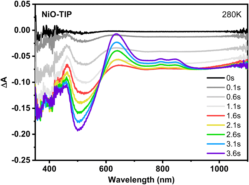
Equivalent measurements for sensitized NiO films (abbreviated as NiO-TIP) were carried out to study the electron hopping at the sensitized NiO interface. In the obtained difference absorption spectrum for NiO-TIP, a shift in wavelengths could be observed most noticeably for the 530 nm and 655 nm features compared to ZrO2-TIP (Fig. 3B). More strikingly, an obvious baseline shift could be also observed, which shifted the isosbestic point towards a negative value. The absorption feature at 0.1 s matches the change in absorption connected to the reduction of NiO surface states, which shows a bleach in the full visible range and displays a peak around 500 nm (ESI,† Fig. S6). The electrochemical reduction behavior of NiO is consistent with previously published results.48
Even though NiO is a p-type semiconductor, and not an insulator like ZrO2, the applied potential step lies within the band gap of the material, which means it should act just like an insulator in the range of the potential step, and one could expect that electron hopping only involves the dyes. However, NiO has surface states within the bandgap,31,33,49 and it is known that NiO surface-associated states can be reduced electrochemically, which manifests in a visual bleach of the NiO films. This creates an overlap of spectral changes due to NiO surface state reduction and to TIP reduction throughout the film, especially just after the potential step was applied. The shift of wavelengths of TIP absorption can therefore primarily be explained by the underlying baseline shift from the reduction of NiO with its peak around 500 nm that shifts the 530 nm and 655 nm features of TIP towards shorter wavelengths. The absorption features at 753 nm and 837 nm of TIP are not shifted as much, because the bleach of NiO surface states shows no distinct peak in this region but rather a flat bleach. It should be noted that differences in magnitude in the difference absorption spectra between ZrO2-TIP and NiO-TIP can be attributed to the difference in film thickness and dye loading. However, since the isosbestic point is maintained and the spectrum just after the potential step shows no contribution of TIP˙−, this is evidence that the reduction of NiO surface states could take place before the reduction of the photosensitizer in the experiment instead of simultaneously which is unexpected.
In order to understand the NiO contribution in sensitized NiO films, single wavelength kinetic traces at 837 nm were recorded. At this wavelength, the dye shows only a rise and the NiO film displays a flat bleach band. This revealed that for pristine NiO films at room temperature, it takes <1 s until the majority of surface states in the film become reduced, reaching a stable equilibrium shortly after the potential step, as shown in Fig. 5A. From the single wavelength kinetic trace of NiO-TIP, it is also clear that the rise due to the formation of TIP˙− only starts after a time delay with respect to the potential onset due to the reduction of NiO. This suggests that upon the onset of the reductive potential step, NiO surface states are first reduced before the electron hopping process occurs between dyes, which then happens much in the same fashion as for dye-sensitized ZrO2 films, as the isosbestic point remains and appears with a time delay.
 | ||
| Fig. 5 (A) Kinetic traces with a time resolution of 33 ms showing the absorption change at 837 nm with time, of various films on FTO in 0.1 M TBAPF6 in acetonitrile upon applying a potential step of 100 mV more positive than the dye E1/2 (TIP/TIP−). (B) Anson plots of NiO and TIP sensitized NiO obtained from spectroelectrochemical measurements with the same potential step as in (A). The shaded areas illustrate the error and the overlaid linear fits are fits to the Cottrell equation for the initial 60% of total absorbance change. | ||
This unexpected possibility of two subsequent processes, where NiO is first reduced before TIP starts being reduced through an electron hopping process, was further investigated with surface passivated NiO films. Reports have shown that NiO surface states or other NiO associated states are involved in the regeneration of dyes and electrolyte,33 and it was important to confirm that NiO surface states do not act as possible dye reduction sites, which is not to be expected. For this, Al2O3-passivated NiO films by atomic layer deposition were prepared, (abbreviated as NiO–Al2O3) since surface passivation through a Al2O3 monolayer has been shown to significantly remove NiO surface states.33,50 The obtained single wavelength kinetic traces of NiO–Al2O3 and NiO–Al2O3-TIP at 837 nm are shown in Fig. 5A. As expected, no change in absorption for the NiO–Al2O3 films was observed, as the majority of surface states were passivated and can no longer be reduced electrochemically. The kinetic trace of NiO–Al2O3-TIP also reveals that the hopping process between TIP molecules is largely unaffected by surface passivation of NiO, and that after the reduction of NiO in NiO-TIP the kinetic traces of NiO-TIP and NiO–Al2O3-TIP match (see Fig. 5A), providing further evidence that NiO reduction occurs swiftly and before TIP reduction. Additionally, the combination of the NiO kinetic trace and NiO–Al2O3-TIP trace in Fig. 5A does not result in the same trace as NiO-TIP which underlines the fact that the NiO reduction and TIP dye reduction do not happen simultaneously but consecutively. To verify FTO as the starting site of electron hopping, e the effect of a NiO blocking layer was investigated which was deposited between FTO and mesoporous NiO. A 100 nm thick compact NiO blocking layer was sputtered onto the FTO surface before deposition of mesoporous NiO and dye sensitization. A much slower reduction process of the dyes through the whole film was observed (Fig. S7, ESI†), indicating that the interaction between dyes and FTO sites are key in the reduction of sensitized films through electron hopping. The bleach attributed to the NiO surface state reduction seemed unaffected by the addition of a blocking layer. In conclusion, blocking the FTO surface underneath the sensitized NiO film proved that FTO is the origin of surface mediated intramolecular electron hopping. Therefore, the electron hopping process for sensitized NiO films with reduced or passivated surface states follows the conventional mechanism for intermolecular charge hopping on other metal oxides.
Taking the underlying spectral change of NiO surface changes into account, Anson Plots for dye sensitized NiO films could be extracted from the spectroelectrochemical data. For this, the most bathochromic absorption feature of TIP˙− at 837 nm was selected, where the spectral change in NiO shows a flat feature. By accounting for the baseline drop at >1000 nm (see ESI,† Section S5), intermolecular hopping rates could be extracted from the normalized and time resolved absorption changes at singular wavelengths. Fitting the linear first 60% of the total change to the Cottrell equation (eqn (1)) gives the apparent diffusion coefficient Dapp at room temperature for intermolecular electron hopping across the NiO-TIP film (Fig. 5B).
From the apparent hopping constant through the film Dapp, the hopping rate khop was calculated with eqn (2), which describes an n-dimensional transport processes depending on the intermolecular distance δ.43,51 In contrast to the literature where the intermolecular distance was estimated through porosity, surface coverage and film thickness,14,20 we calculated the average distance between TIP dyes directly from the BET surface area of the films and determined dye loading from de-loading experiments with eqn (5).
 | (5) |
This yielded an experimental determined average center-to-center distance between the TIP dyes of approximately 12 Å on the NiO film (see ESI† for more details). These intermolecular distances are comparable with the values reported for TiO2 sensitized films.13,20,52
Theoretical modelling of the TIP dye molecules on the NiO surface was obtained by optimization using a MM3 force field, as shown in Fig. 6. Fig. 6A shows the optimized structure in the presence of solvent (acetonitrile). Fig. 6B and C show the TIP dye molecules adsorbed onto the NiO surface replacing the adsorbed solvent. From these images, we can deduce that the TIP dye molecules are adsorbed perpendicularly to the NiO surface in the presence of acetonitrile. The typical inter-molecule distances are in the range 11.7 Å to 12.0 Å, which is close to the average distance obtained from experiment.
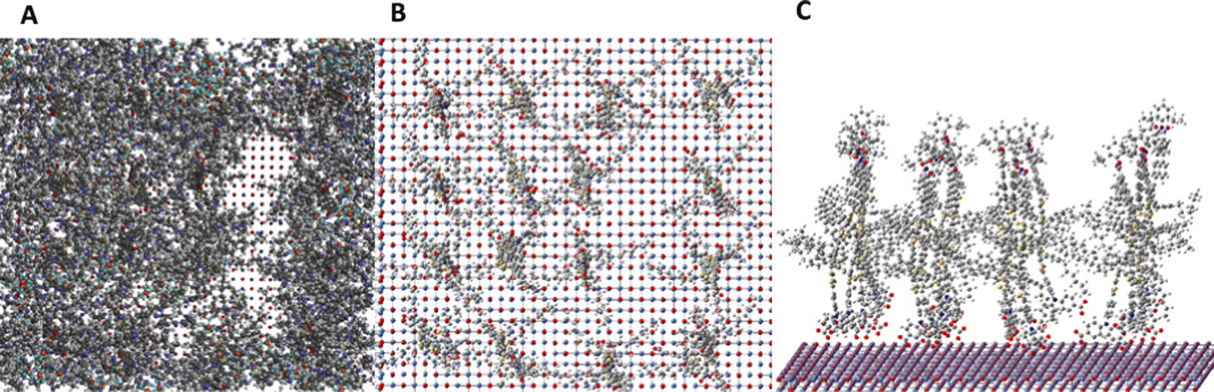 | ||
| Fig. 6 The distribution of TIP dye molecules on an ideal NiO surface (A) in the presence of solvent, (B and C) in the absence of solvent. | ||
In the literature on hole hopping on metal oxide surfaces, the dimensionality is typically assumed to be n = 314,20 which means that a charge at any point has the possibility to move freely in all three dimensional directions, with the same probability. Vaissier et al.53 have estimated the effective diffusion coefficient across a randomly oriented surface by combining a two dimensional hopping rate with an estimated surface diffusion coefficient. This yielded a result similar to the standard result for hopping within a three-dimensional lattice. However, they also noted that n is likely lower in reality due to film geometry and defects, the tortuosity of the surfaces, constricted interparticle connections and incomplete connectivity between dyes. In reality, the effective diffusion coefficient across surfaces in a mesoporous 3-dimensional structure lies likely somewhere between n = 2 and n = 3. We have therefore reported the extracted hopping rates for both n = 2 and n = 3. The results are summarized in Table 1. One can see that there is no significant difference in hopping rates between two-dimensional and three-dimensional models.
| E 1/2 (V vs. Ag/AgNO3) | D app (m2 s−1) | δ (Å) | k hop (s−1) for n = 3 | k hop (s−1) for n = 2 | |
|---|---|---|---|---|---|
| TIP | 1.21 | 8.0 ± 1.2 × 10⁻¹⁴ | 12 ± 1 | 3.6 ± 1.5 × 10⁵ | 2.4 ± 1.2 × 10⁵ |
| NiO surface states | — | 1.8 ± 0.6 × 10⁻¹² | 5.3 ± 0.5 | 3.9 ± 1.1 × 10⁷ | 2.6 ± 0.9 × 10⁷ |
To further study the electron hopping between the TIP dyes on the NiO surface, time-resolved spectroelectrochemistry was performed in the range of 272 K to 303 K. The obtained apparent electron diffusion coefficients at various temperatures from the individual Anson's plots are shown in Fig. 7. The data was fit to the expression of a thermally activated process with eqn (6), where Eact is the activation energy.
 | (6) |
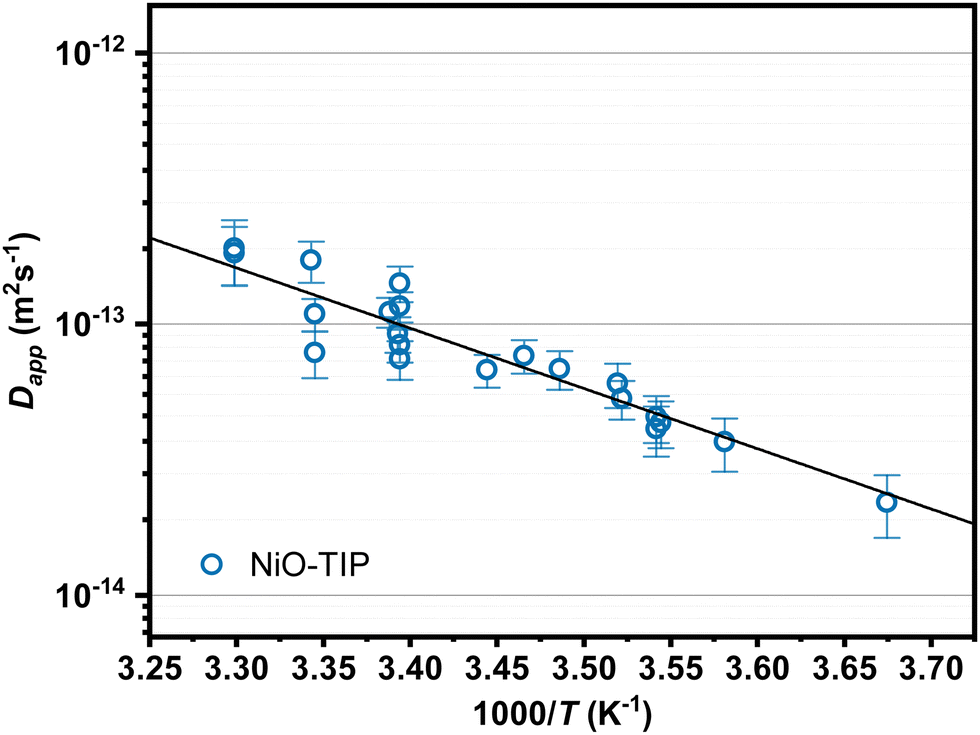 | ||
| Fig. 7 Temperature dependent values of the electron apparent diffusion coefficient (Dapp) extracted from spectroelectrochemistry performed on TIP sensitized NiO films on FTO in 0.1 M TBAPF6 in acetonitrile. Linear fits of the data allow determination of the activation energy and reorganization energy. | ||
| Dye | λ experimental (eV) | E act (meV) | H AB (meV) for n = 2 | H AB (meV) for n = 3 |
|---|---|---|---|---|
| TIP | 1.77 ± 0.16 | 444 ± 46 | 33 ± 14 | 40 ± 14 |
Since the difference in hopping rates for 2D and 3D diffusion is just a factor and corresponds to the same apparent diffusion constant, the determined reorganization energy is the same for both hopping orders. The value for the reorganization energy for the intermolecular electron hopping for the TIP dye obtained from temperature dependent spectroelectrochemistry measurements is relatively high with 1.77 eV in comparison to the reported values for n-type dyes in the literature (up to 1.54 eV for D131, an indoline based organic dye).13,14 However, it has also been found that for hole hopping, the size of the HOMO is affecting the reorganization energy, where a more delocalized system exhibits lower reorganization energy.13 For electron hopping, it is likely that the LUMO plays a role, which for TIP is localized on the perylene monoimide acceptor unit,34 and makes up a comparably small part of the dye and should be located furthest away from the surface in the electrolyte, as visualized in Fig. 2B. Bangle et al.55 have also shown that the reorganization energy increases for molecules with a variable bridge unit if the interfacial electron transfer occurs further away from the electrode surface and that the solvent reorganization increases to bulk values when the transfer happens outside of the electric double layer. As the TIP dye is a relatively large photosensitizer and electron hopping is assumed to take place between the PMI subunit, it is possible that the relatively large distance to the NiO surface influences the reorganization energy and that lateral electron hopping may even occur outside of the electric double layer. Considering the size of the LUMO and overall size of the molecule, a large outer-sphere reorganization energy is to be expected, especially in a very polar solvent, such as acetonitrile or electrolytes that are typical in DSSCs and is in agreement with the experimentally observed value.13,53
Theoretical calculations of the rate constants of electron hopping between TIP dye molecules were carried out based on Marcus theory,56,57 using eqn (4). The electronic coupling (HAB) of electron hopping between TIP dyes in this context is taken as the coupling between the lowest unoccupied molecular orbitals (LUMOs) of the TIP molecules.
The electronic coupling and rate constants of electron hopping between the TIP molecules using the reorganization energy obtained from the theoretical estimation, 0.17 eV, and from experimental results, 1.77 eV, respectively were calculated using semiempirical density function theory with snapshots extracted at every 0.05 ps with a total simulation length of 300 ps (figures in ESI†). It is clear that the experimental reorganization energy is considerably higher than that obtained from theoretical calculations. This indicates that the real-life reorganization is affected considerably by the chemical environment of the TIP molecules, and that an ideal model consisting of two TIP molecules is too simple to mimic reality in this system. The environmental effects may for instance involve the adsorption interaction with the NiO surface and possibly dye aggregation. In any case, most likely the experimental reorganization energy represents a better estimate to be used in the evaluation of the dynamical rate constants. The dynamic electronic coupling with respect to electron hopping between the TIP molecules as obtained from the ADF calculation ranges from 10−2 ∼ 23.4 meV. The dynamic rate constants of electron hopping using the theoretical reorganization energy of 0.17 eV range between 107 ∼ 4.23 × 10¹² s−1. However, if instead the dynamic rate constants of electron hopping are evaluated using the experimental reorganization energy of 1.77 eV, a range of 4.6∼ 2.5 × 10⁵ s−1 is obtained with a weighted average of 2.4 × 10⁴ s−1. The latter estimate is more consistent with the rate of electron hopping obtained from experiment, 3.6 × 10⁵ s−1. Yet, there is a difference and the slightly larger electron hopping rates indicated by the experimental results may offer some information regarding deviations from ideality regarding hopping pathways in the two-dimensional film formed by the TIP molecules. Making an analogy to the reduction of diffusion in porous materials because of tortuosity, one can make estimates of the formal porosity in terms of effective diffusion or hopping pathways available to a single TIP molecule in the two-dimensional film. Such estimates indicate a porosity around 15%, which means that the available pathways of electron hopping only is in the order of 1/7 with respect to an ideal dye film and thus that the defect density is quite high. More details of the porosity estimate are given in the ESI.†
Beside the intermolecular electron hopping between dyes immobilized on the NiO surface, the reduction of NiO surface states was also investigated. As bulk NiO is not electron conductive, it was assumed that the mechanism for reduction is electron hopping on the NiO surface between surface-associated states. For this, ms-time resolved single wavelength kinetic traces at 520 nm and 837 nm were recorded for pristine NiO films, utilizing the electrochromic behavior related to these surface states.48 As the kinetic behavior was the same, only the 837 nm traces are shown in Fig. 5B. The kinetic traces were fitted and Dapp was extracted. To obtain the distance of states for calculation of the electron transfer rate between NiO surface states, the density of states (DOS) on the surface was determined from the cathodic part of the CV curve of pristine NiO (Fig. S9, ESI†). This yielded a concentration of surface states on the NiO surface of 3.4 nm−2, or an average distance between states of 5.3 Å (see ESI† for calculation) with which an electron hopping rate between the NiO surface states could be calculated with eqn (2). The results are summarized in Table 1. Notably, complete reduction of NiO surface states in the film occurs much faster than the reduction of TIP dye on the surface, by approximately two orders of magnitude.
Considering the reduced nature of NiO films during our investigations, it may be possible that its surface states can mediate or hinder electron transfer. For example, for highly doped oxide materials such as fluorine doped tin oxide (FTO), it has been shown that the surface itself can mediate electron transfer, however it is unclear how other semiconductors behave.12 Another example is TiO2 which becomes more conductive with a negative applied potential, and thus may mediate self-exchange reactions.58 In contrast, NiO becomes less conductive when the surface states are passivated,33 and should therefore not mediate intermolecular electron self-exchange rates. This also means that further studies may be necessary to understand intermolecular electron hopping between dyes on NiO in real systems where the surface states are not electrochemically reduced or passivated.
From temperature-dependent spectroelectrochemistry of NiO-TIP, it was also noticeable that the absorption spectra at lower temperatures show an increase in the time delay between the onset of the reductive potential step and the beginning of TIP reduction. At 280 K, the initial (0–1.1 s) baseline shift is noticeably slower than at room temperature but maintains its pure NiO nature with minimal TIP contribution visible in wavelengths >700 nm where NiO absorption is flat (Fig. 8), whereas the features of dye reduction dominate the evolution at t > 1s and exhibit an isosbestic point. This furthermore supports our hypothesis that NiO is first reduced and then the lateral TIP hopping starts.
 | ||
| Fig. 8 Time resolved spectroelectrochemistry (SEC) measurements showing the difference absorption spectra recorded before and after a potential step of −1.31 V vs. Ag/AgNO3 at 280 K of NiO-TIP films in 0.1 M TBAPF6 acetonitrile. | ||
While the data clearly show the fast reduction of NiO before the reduction of the TIP dye begins, it is unclear why this lag time is observed. It may be possible that dyes close to the FTO surface are reduced simultaneous with the NiO surface states but immediately inject their electron to a nearby “neutral” NiO surface state and are thus not spectrally visible.
Another possibility may be that the charge is flowing through the NiO surface states first due to a lower resistance, as the intramolecular electron hopping and surface state mediated electron transport can be considered as two parallel processes in a corresponding electrical circuit. Since the distance between the surface states is shorter and the solvent reorganization energy can be expected to be lower than for intermolecular electron hopping further away from the surface, experiencing bulk solvent dielectric constants the resistance for the NiO surface states should be lower. While it is unclear if the dyes on the NiO surface are involved in the process of NiO surface state reduction (shown as grey arrows in the first step of NiO reduction in Fig. 9), we can exclude from our data that NiO surface states are involved in the reverse reaction, i.e. reduction of TIP dye, and are sure that the intermolecular electron hopping starts at the FTO surface.
 | ||
| Fig. 9 Proposed schematic for electrochemically induced charge transfer processes for sensitized NiO films with NiO surface associated states. Active surface states are depicted in brown, passivated/reduced surface states are colored in grey. | ||
In any case, considering the “lag time” observed for dye sensitized NiO films that exhibit surface-states, the conventional mechanism for electrochemically induced electron hopping must be expanded with an inter-surface-state charge transfer process that occurs before intermolecular electron hopping. The proposed mechanism for applying a reductive potential step to dye-sensitized NiO films is (1) reduction of NiO surface states through inter-surface state electron transfer until the majority of surface states are reduced and (2) reduction of dye close to the FTO surface and is followed by intermolecular electron transfer across the NiO surface, as depicted in Fig. 9.
As processes in dye-sensitized NiO photocathodes in solar devices are typically light induced, it remains unclear what the mechanism for photo-induced charge transfer at the NiO-dye interface looks like. However, we can assume that the intermolecular hopping rate between the TIP dyes should be comparable, as well as the large reorganization energy in a polar medium which is typical for dye sensitized solar cell electrolytes. Possible differences in photo-induced charge transfer will likely stem from the NiO surface states that should be largely empty when no potential is applied. The fast injection of electrons from dyes to NiO surface states should compete with the electron hopping processes between dyes, and it is likely that the electron on the molecule recombines quickly with a previously injected hole in NiO. Since the observed hopping rate between the dyes in our study, occurring on the μs-scale, is comparatively slow to the dye regeneration, these findings suggest that intermolecular electron hopping might not play a significant role in real p-type dye sensitized devices such as solar cells or even PEC devices. For solar cells, the reported dye regeneration rates in the literature, assuming by electron transfer from the reduced dye to the electrolyte, are typically at least an order of magnitude faster than hopping and range from sub-nanosecond,59 mostly in the nanosecond range, with a few examples occurring in the range of microseconds.60 For PEC cells, the charge transfer to the photocatalyst can take place on the sub-picosecond scale,25 although in many cases it could occur much slower.
What is possibly even more significant for both devices is our previous proposal that the reduced dye is short lived due to electron transfer into non-reduced surface states in the NiO.33 This makes for a slightly different working mechanism for p-type dye sensitized devices where the reduced dye is not regenerated by the electrolyte but instead by NiO, which is then regenerated by the electrolyte in a second step. As the charge transport rate of the electrons in the surface states are much faster, we hypothesize that other charge transport processes than lateral inter-dye electron hopping could dominate in real cells. From our data, it seems that electron hopping between NiO surface states is favored over intermolecular electron hopping. This can potentially have significant consequences for the performance of full devices: upon excitation, it is widely assumed that the p-type dye injects a hole into NiO and is reduced; if some of the electrons on the dyes are then injected into the NiO surface states, it is possible that the fast-moving electrons in the NiO surface states recombines with the hole that had been previously injected into NiO, before being regenerated by the electrolyte.
In other dyes-based systems where the electron hopping rate could be much faster than that between TIP dyes, it is possible that electron hopping could play an important role during photophysical processes in p-type dye sensitized solar cells or PEC devices for solar fuels. More studies on different dyes and electrolytes are therefore desirable.
Conclusion
The characterization of electron hopping processes at a TIP dye sensitized NiO surface with spectroelectrochemical methods has provided new insights into the kinetics of hopping and charge transfer processes of p-type dye sensitized photocathodes. Two main electron hopping pathways across a dye-sensitized NiO surface could be identified: (i) intermolecular electron hopping between the immobilized dyes and (ii) electron hopping between NiO surface states. The rates of electron hopping between NiO surface states was found to occur on the nanosecond time scale, which is two orders of magnitude faster than electron hopping between TIP dyes, occurring on the microsecond time scale. Our results suggest that electron hopping between NiO surface states is the favored pathway in the TIP dye sensitized NiO film during an applied potential step in spectroelectrochemical measurements. A rarely observed sequential behavior of the two processes was also observed with an applied potential: only once the majority of NiO surface states are reduced via electron hopping between the surface states, then intermolecular electron hopping between the dyes immobilized on the NiO surface starts.A key conclusion of this study is that charge transport in the NiO semiconductor dominates and is likely important for p-type dye-sensitized solar cells. From our findings, it can be hypothesized that if intermolecular electron hopping between the immobilized dyes occurs on the μs time scale, it is then much slower than dye regeneration and may therefore not play a significant role in dye-sensitized solar cells or solar fuel devices. This is an new finding as compared to what has been observed for some dye-sensitized photoanodes.20 In contrast, the fast electron hopping between NiO surface states could be of importance for charge transport to the back contact in devices. This would provide much better conduction than what is expected from the poor bulk conductivity of NiO, and would be in line with proposed mechanisms from the literature and observations from conductivity measurements.33,48,61 It is possible, however, that the fast electron hopping process between NiO surface states also potentially promotes charge recombination between the injected electrons in NiO surface states from excited dyes30 and photo-injected holes in NiO. More studies on different dyes are necessary to be carried out to investigate if there is a possibility that the electron hopping between dyes on NiO could occur much faster than for TIP and show a significant influence in photophysical processes in dye-sensitized NiO based solar cell and solar fuel devices.
Data availability
Experimental data and detailed experimental procedures are available in the ESI.†Author contributions
S. W. and H. T. formulated and designed this project. S. W. designed the experiments, did data curation and carried out the investigation. L. He. and L. K. performed theoretical modelling and simulations. H. T. was supervising this project, G. B. and L. Ha. co-supervised and provided valuable ideas and scientific discussion. All authors were involved in interpreting the results. S. W. prepared the manuscript with help from L. He. and all authors helped revise the paper.Conflicts of interest
The authors declare no conflict of interest.Acknowledgements
We would like to gratefully thank the Swedish Energy Agency (49278-1) for financial support. We would also like to thank Ashley Castner for helping with BET surface measurements of NiO; Dr Bo Xu for the synthesized TIP dye, and Dr Carl Hägglund for his support with ALD procedures and knowledge. Mr Johan Nordstrand is gratefully acknowledged for valuable input regarding modelling of tortuosity and porosity in low-dimensional systems. We acknowledge the National Supercomputer Centre at Linköping University for computational resources.References
- M. Hoel and S. Kverndokk, Resour. Energy Econ., 1996, 18, 115–136 CrossRef.
- M. Höök and X. Tang, Energy Policy, 2013, 52, 797–809 CrossRef.
- J. T. Roberts, Soc. Nat. Resour., 2001, 14, 501–509 CrossRef.
- N. S. Diffenbaugh and M. Burke, Proc. Natl. Acad. Sci. U. S. A., 2019, 116, 9808–9813 CrossRef PubMed.
- B. O’Regan and M. Grätzel, Nature, 1991, 353, 737–740 CrossRef.
- F. Lakadamyali, A. Reynal, M. Kato, J. R. Durrant and E. Reisner, Chem. – Eur. J., 2012, 18, 15464–15475 CrossRef PubMed.
- Z. Yu, F. Li and L. Sun, Energy Environ. Sci., 2015, 8, 760–775 RSC.
- C. S. Tao, J. Jiang and M. Tao, Sol. Energy Mater. Sol. Cells, 2011, 95, 3176–3180 CrossRef.
- S. Wrede and H. Tian, Phys. Chem. Chem. Phys., 2020, 22, 13850–13861 RSC.
- S. Zhang, H. Ye, J. Hua and H. Tian, EnergyChem, 2019, 1, 100015 CrossRef.
- K. Sharma, V. Sharma and S. S. Sharma, Nanoscale Res. Lett., 2018, 13, 1–46 CrossRef PubMed.
- K. Hu and G. J. Meyer, Langmuir, 2015, 31, 11164–11178 CrossRef PubMed.
- D. Moia, V. Vaissier, I. López-Duarte, T. Torres, M. K. Nazeeruddin, B. C. O’Regan, J. Nelson and P. R. F. Barnes, Chem. Sci., 2014, 5, 281–290 RSC.
- B. N. DiMarco, T. C. Motley, R. S. Balok, G. Li, M. A. Siegler, R. M. O’Donnell, K. Hu and G. J. Meyer, J. Phys. Chem. C, 2016, 120, 14226–14235 CrossRef.
- S. A. Trammell and T. J. Meyer, J. Phys. Chem. B, 1999, 103, 104–107 CrossRef.
- P. Bonhôte, E. Gogniat, S. Tingry, C. Barbé, N. Vlachopoulos, F. Lenzmann, P. Comte and M. Grätzel, J. Phys. Chem. B, 1998, 102, 1498–1507 CrossRef.
- S. Günes, H. Neugebauer and N. S. Sariciftci, Chem. Rev., 2007, 107, 1324–1338 CrossRef.
- S. Ardo and G. J. Meyer, J. Am. Chem. Soc., 2010, 132, 9283–9285 CrossRef.
- S. Ardo and G. J. Meyer, J. Am. Chem. Soc., 2011, 133, 15384–15396 CrossRef.
- M. D. Brady, L. Troian-Gautier, T. C. Motley, M. D. Turlington and G. J. Meyer, ACS Appl. Mater. Interfaces, 2019, 11, 27453–27463 CrossRef PubMed.
- D. Moia, T. Leijtens, N. Noel, H. J. Snaith, J. Nelson and P. R. F. Barnes, Adv. Mater., 2015, 27, 5889–5894 CrossRef PubMed.
- J. W. Youngblood, S. H. A. Lee, Y. Kobayashi, E. A. Hernandez-Pagan, P. G. Hoertz, T. A. Moore, A. L. Moore, D. Gust and T. E. Mallouk, J. Am. Chem. Soc., 2009, 131, 926–927 CrossRef.
- D. Moia, A. Szumska, V. Vaissier, M. Planells, N. Robertson, B. C. O’Regan, J. Nelson and P. R. F. Barnes, J. Am. Chem. Soc., 2016, 138, 13197–13206 CrossRef.
- R. N. Sampaio, A. V. Müller, A. S. Polo and G. J. Meyer, ACS Appl. Mater. Interfaces, 2017, 9, 33446–33454 CrossRef.
- A. M. Brown, L. J. Antila, M. Mirmohades, S. Pullen, S. Ott and L. Hammarström, J. Am. Chem. Soc., 2016, 138, 8060–8063 CrossRef.
- M. G. Gatty, S. Pullen, E. Sheibani, H. Tian, S. Ott and L. Hammarström, Chem. Sci., 2018, 9, 4983–4991 RSC.
- N. Kaeffer, C. D. Windle, R. Brisse, C. Gablin, D. Leonard, B. Jousselme, M. Chavarot-Kerlidou and V. Artero, Chem. Sci., 2018, 9, 6721–6738 RSC.
- A. G. Marrani, V. Novelli, S. Sheehan, D. P. Dowling and D. Dini, ACS Appl. Mater. Interfaces, 2014, 6, 143–152 CrossRef.
- C. J. Flynn, S. M. McCullough, L. Li, C. L. Donley, Y. Kanai and J. F. Cahoon, J. Phys. Chem. C, 2016, 120, 16568–16576 CrossRef.
- L. D’Amario, J. Föhlinger, G. Boschloo and L. Hammarström, Chem. Sci., 2017, 9, 223–230 RSC.
- L. D’Amario, R. Jiang, U. B. Cappel, E. A. Gibson, G. Boschloo, H. Rensmo, L. Sun, L. Hammarström and H. Tian, ACS Appl. Mater. Interfaces, 2017, 9, 33470–33477 CrossRef.
- K. Zhu, S. K. Frehan, G. Mul and A. Huijser, J. Am. Chem. Soc., 2022, 144, 11010–11018 CrossRef PubMed.
- L. Tian, R. Tyburski, C. Wen, R. Sun, M. Abdellah, J. Huang, L. D’Amario, G. Boschloo, L. Hammarström and H. Tian, J. Am. Chem. Soc., 2020, 142, 18668–18678 CrossRef.
- B. Xu, S. Wrede, A. Curtze, L. Tian, P. B. Pati, L. Kloo, Y. Wu and H. Tian, ChemSusChem, 2019, 12, 3243–3248 CrossRef PubMed.
- E. Sheibani, L. Zhang, P. Liu, B. Xu, E. Mijangos, G. Boschloo, A. Hagfeldt, L. Hammarström, L. Kloo and H. Tian, RSC Adv., 2016, 6, 18165–18177 RSC.
- X. Li, M. K. Nazeeruddin, M. Thelakkat, P. R. F. Barnes, R. Vilar and J. R. Durrant, Phys. Chem. Chem. Phys., 2011, 13, 1575–1584 RSC.
- Q. Wang, S. M. Zakeeruddin, J. Cremer, P. Bäuerle, R. Humphry-Baker and M. Grätzel, J. Am. Chem. Soc., 2005, 127, 5706–5713 CrossRef CAS.
- S. A. Trammell and T. J. Meyer, J. Phys. Chem. B, 1999, 103, 104–107 CrossRef.
- A. J. Bard and L. R. Faulkner, Fundamentals and applications, Wiley, New York, NY, 2nd edn, 2001 Search PubMed.
- F. G. Cottrell, Z. Phys. Chem., 1903, 42U, 385–431 CrossRef.
- F. C. Anson, D. N. Blauch, C. F. Shu, J. M. Savéant and J. M. Savéant, J. Am. Chem. Soc., 1991, 113, 1922–1932 CrossRef.
- P. G. Hoertz, A. Staniszewski, A. Marton, G. T. Higgins, C. D. Incarvito, A. L. Rheingold and G. J. Meyer, J. Am. Chem. Soc., 2006, 128, 8234–8245 CrossRef PubMed.
- I. Ruff and L. Botár, J. Chem. Phys., 1985, 83, 1292–1297 CrossRef.
- V. Vaissier, E. Mosconi, D. Moia, M. Pastore, J. M. Frost, F. De Angelis, P. R. F. Barnes and J. Nelson, Chem. Mater., 2014, 26, 4731–4740 CrossRef CAS.
- L. Favereau, J. Warnan, Y. Pellegrin, E. Blart, M. Boujtita, D. Jacquemin and F. Odobel, Chem. Commun., 2013, 49, 8018–8020 RSC.
- Y. Farré, L. Zhang, Y. Pellegrin, A. Planchat, E. Blart, M. Boujtita, L. Hammarström, D. Jacquemin and F. Odobel, J. Phys. Chem. C, 2016, 120, 7923–7940 CrossRef.
- L. Tian, J. Föhlinger, Z. Zhang, P. B. Pati, J. Lin, T. Kubart, Y. Hua, J. Sun, L. Kloo, G. Boschloo, L. Hammarström and H. Tian, Chem. Commun., 2018, 54, 3739–3742 RSC.
- G. Boschloo and A. Hagfeldt, J. Phys. Chem. B, 2001, 105, 3039–3044 CrossRef.
- L. D’Amario, J. Föhlinger, G. Boschloo and L. Hammarström, Chem. Sci., 2018, 9, 223–230 RSC.
- C. J. Flynn, S. M. McCullough, E. Oh, L. Li, C. C. Mercado, B. H. Farnum, W. Li, C. L. Donley, W. You, A. J. Nozik, J. R. McBride, T. J. Meyer, Y. Kanai and J. F. Cahoon, ACS Appl. Mater. Interfaces, 2016, 8, 4754–4761 CrossRef PubMed.
- L. Botár and I. Ruff, Chem. Phys. Lett., 1988, 149, 99–101 CrossRef.
- K. Hu, K. C. D. Robson, E. E. Beauvilliers, E. Schott, X. Zarate, R. Arratia-Perez, C. P. Berlinguette and G. J. Meyer, J. Am. Chem. Soc., 2014, 136, 1034–1046 CrossRef CAS.
- V. Vaissier, P. Barnes, J. Kirkpatrick and J. Nelson, Phys. Chem. Chem. Phys., 2013, 15, 4804 RSC.
- P. Vath, M. B. Zimmt, D. V. Matyushov and G. A. Voth, J. Phys. Chem. B, 1999, 103, 9130–9140 CrossRef.
- R. E. Bangle, J. Schneider, D. T. Conroy, B. M. Aramburu-Trošelj and G. J. Meyer, J. Am. Chem. Soc., 2020, 142, 14940–14946 CrossRef PubMed.
- R. A. Marcus, J. Chem. Phys., 1956, 24, 979–989 CrossRef.
- N. S. Hush, J. Chem. Phys., 1958, 28, 962–972 CrossRef.
- A. Staniszewski, A. J. Morris, T. Ito and G. J. Meyer, J. Phys. Chem. B, 2007, 111, 6822–6828 CrossRef PubMed.
- A. Morandeira, G. Boschloo, A. Hagfeldt and L. Hammarström, J. Phys. Chem. C, 2008, 112, 9530–9537 CrossRef.
- E. Benazzi, J. Mallows, G. H. Summers, F. A. Black and E. A. Gibson, J. Mater. Chem. C, 2019, 7, 10409–10445 RSC.
- L. D’Amario, G. Boschloo, A. Hagfeldt and L. Hammarström, J. Phys. Chem. C, 2014, 118, 19556–19564 CrossRef.
Footnote |
| † Electronic supplementary information (ESI) available. See DOI: https://doi.org/10.1039/d2cp03249j |
| This journal is © the Owner Societies 2022 |