
Coupling of plasmonic nanoparticles on a semiconductor substrate via a modified discrete dipole approximation method†
Diogo F.
Carvalho
 *a,
Manuel A.
Martins
b,
Paulo A.
Fernandes
acd and
M. Rosário P.
Correia
a
*a,
Manuel A.
Martins
b,
Paulo A.
Fernandes
acd and
M. Rosário P.
Correia
a
ai3N, Department of Physics, University of Aveiro, 3810-193 Aveiro, Portugal. E-mail: diogocarvalho@ua.pt
bCICECO, Department of Materials and Ceramic Engineering, University of Aveiro, 3810-193 Aveiro, Portugal
cINL – International Iberian Nanotechnology Laboratory, 4715-330 Braga, Portugal
dCIETI, Department of Physics, ISEP – Porto School of Engineering, 4200-072, Portugal
First published on 28th June 2022
Abstract
Understanding the plasmonic coupling between a set of metallic nanoparticles (NPs) in a 2D array, and how a substrate affects such coupling, is fundamental for the development of optimized optoelectronic structures. Here, a simple semi-analytical procedure based on discrete dipole approximation (DDA) is reported to simulate the far-field and near-field properties of arrays of NPs, considering the coupling between particles, and the effect of the presence of a semiconductor substrate based on the image dipole approach. The method is validated for Ag NP dimers and single Ag NPs on a gallium nitride (GaN) substrate, a semiconductor widely used in optical devices, by comparison with the results obtained by the finite element method (FEM), indicating a good agreement in the weak coupling regime. Next, the method is applied to square and random arrays of Ag NPs on a GaN substrate. The increase in the surface density of NPs on a GaN substrate mainly results in a redshift of the dipolar resonance frequency and an increase in the near-field enhancement. This model, based on a single dipole approach, grants very low computational times, representing an advantage to predict the optical properties of large NP arrays on a semiconductor substrate for different applications.
Introduction
Since the end of the 20th century, there has been an increase in the number of studies with metallic nanoparticles (NPs) in several areas of science, namely in photovoltaic devices,1,2 light-emitting devices,3 imaging and sensing applications,4,5 surface-enhanced Raman spectroscopy (SERS),6,7etc., mainly due to the very interesting optical properties related to the plasmonic phenomena and the development of synthesis and nanomanipulation techniques of NPs. The outstanding optical properties of NPs arise due to the interaction with electromagnetic radiation. Under resonance conditions, the conduction electrons within the NPs oscillate at an external field frequency, known as localized surface plasmon resonance (LSPR). The LSPR frequency, typically ranging from the near-ultraviolet to the near-infrared region, is highly tunable due to the dependence on the NP chemical composition, size, shape, and surrounding medium.8 The localized surface plasmons result in a strong scattering and absorption of electromagnetic radiation under LSPR conditions, and a phenomenon of near-field enhancement,9 providing a wide platform of research.In most studies, NPs are close enough to interact with each other, and thus the study of this coupling between NPs is fundamental for the development of optimized optical structures. Several theoretical and experimental studies of the coupling between two or more NPs have been published.10–16 Some near- and far-field phenomena related to this coupling are well established, such as the redshift of the LSPR as the gap distance decreases, for an incident electric field parallel to the alignment of the NPs, or the enhanced electric field in the gap between NPs. This near-field enhancement of coupled NPs has been applied to improve the SERS enhancement factor for a highly sensitive detection of molecules adsorbed in the gap between NPs.17–19 The LSPR frequency variation with the coupling between NPs also influences the SERS enhancement factor due to the matching condition with the excitation and/or Raman scattering frequency of the photons.20
Computation of the far-field and near-field characteristics of isolated spherical NPs is relatively simple with Mie theory,21 an exact solution to Maxwell's equations for spherical particles. Mie theory easily describes the LSPR dependence on the size of NPs, namely the redshift and broadening of the plasmon peak as the particle size increases, as well as the appearance of higher resonance modes.11 For widely separated NPs, these behave independently, however, for an assembly of NPs, the isolated NP assumption is most of the time not valid. For coupled NPs, there are two main interaction regimes. The weak coupling regime results in a redshift of the dipolar LSPR mode, as the gap between NPs decreases, due to the depolarization of the NPs’ charge oscillations induced by the coupling. For even smaller gaps (nearly touching), a strong coupling regime emerges, in which higher frequency multipolar modes appear, as a result of the non-uniform field induced in each of the NPs.12,22
Several studies have been conducted to describe the coupling between NPs based on different methods. T-matrix multiparticle-scattering theory is a generalized multiparticle Mie solution based on the superposition of individual solutions in the form of vector spherical harmonic expansion.23–26 Another widely used method is discrete dipole approximation (DDA).11,16,27–29 It is a semi-analytical method to obtain the optical properties for one or more NPs of an arbitrary shape, in which the NPs are described by an array of small dipoles. Other numerical methods have also been used, including the finite difference time domain (FDTD) method30–34 or the finite element method (FEM).15,35–39 These analytical and numerical approaches generally give rise to an accurate solution, but result in a very time-consuming process for large arrays of NPs; thus, these models have been used to study the coupling between a small number of NPs.
The presence of a substrate near to the NP surface also affects significantly its optical properties due to the induced field in the substrate, although this effect is often neglected in the literature.40 As with the coupling between NPs, there is a redshift of the LSPR and a large near-field enhancement in the gap between the NPs and the substrate,41–44 resulting in a gap-dependent SERS enhancement factor.45,46 The interaction with a metallic substrate is complex due to the formation of propagating surface plasmon polaritons at the surface of the substrate; therefore, the coupling is generally studied by numerical approaches.47,48 For a dielectric substrate, the interaction has been treated in a simple way through the image dipole approach,49–51 within quasistatic approximation, applied for NP sizes much smaller than the wavelength of radiation. For small NPs, this method has shown a good agreement with the experimental results and numerical approaches.50,52 Although it allows the study of semiconductor substrates with a non-negligible imaginary component of permittivity, the studies in the literature are scarce.44 Other more complex analytical models, based on the multipolar coupling between the NPs and the substrate,53,54 have been developed, although simpler analytical approaches are always preferable. Therefore, it is important to explore new ways to extend the size validity range of dipolar approximation, for example, by calculating the polarizability of the NPs by means of a new expression, different from the general Rayleigh (or Clausius–Mossotti) polarizability in quasistatic approximation. In this sense, several authors have proposed different corrections for the Rayleigh polarizability, namely radiative-reaction correction55,56 or effective volume correction.57 However, it has been shown that these corrections can even result in less accurate calculations for certain size ranges.58 Kuwata et al.59 developed an empirical formula for the polarizability of an ellipsoid, able to predict the LSPR redshift due to dynamic depolarization60 and broadening caused by radiation damping61 with increasing NP size, not predicted by the Rayleigh polarizability. For quick computing algorithms, the Kuwata polarizability is especially useful when it is intended to study the optical properties of a set of NPs, using dipolar approximation, allowing more accurate results than Rayleigh polarizability.
In most applications, NPs tend to interact in two-dimensional (2D) arrays. The random distribution of NPs is the most common in technological applications, especially for NPs synthesized by wet-chemical methods,62,63 thermal annealing,64–66etc. Fabrication of ordered structures is also possible through lithographic67–70 or self-assembly71,72 methods. The coupling between a set of NPs in 2D arrays can significantly alter the response of the NPs due to the superposition of the interaction phenomena between NPs and the formation of delocalized surface modes along the arrays.73,74 There have been many theoretical studies with 2D arrays of NPs,34,38,40,74 although generally for a small number of NPs or infinite periodic arrays, due to the very time-consuming process of the analytical and numerical methods used.
In this paper, a semi-analytical procedure based on DDA is developed to calculate the far-field and near-field properties of square and random arrays of Ag NPs, considering the weak coupling between the NPs and the influence of a substrate, based on the image dipole approach.28 In our calculations, each NP is represented by a single dipole, unlike the most general DDA implementation, with the polarizability calculated using the empirical formula of Kuwata.73 Our approach enables the study of arrays of NPs up to ∼80 nm in size. Our single-dipole model permits very quick computations for arrays of hundreds of NPs, unlike numerical approaches, and to predict the effect of a dielectric or semiconductor substrate. We consider the presence of a gallium nitride (GaN) substrate in our calculations, a semiconductor widely used in optical devices. Some NP coupling studies with GaN films and GaN-based quantum wells with the purpose of increasing the emission efficiency63,65,67,75,76 and as SERS substrates77–80 have been published, but the influence of the spatial arrangement of the NPs and the substrate on the LSPR has not been sufficiently explored. Preliminary results for NP dimers and a single NP on a GaN substrate are compared with those obtained by FEM, indicating a good agreement in the weak coupling regime. We demonstrate a redshift and a widening of the LSPR mode with the GaN substrate and with increasing surface density of NP arrays. The randomness in the distribution of the NPs mainly results in the extinction of the standing modes of the square arrays, as expected. The described model provides new insights into the weak coupling in large arrays of NPs on a semiconductor substrate.
Theoretical methods
Dipolar approximation
At the limit where the size of a NP is much smaller than the wavelength of the incident radiation, the NP is exposed to a nearly uniform field, throughout the region of the space it occupies. Thus, the interaction of light with the NP can be described by electrostatics. This approach is called quasistatic or dipolar approximation (also called Rayleigh approximation, for spherical NPs). In this approach, the incidence of a uniform electric field E0 results in the formation of an electric dipole moment21p = εαE0 within the NP, where ε is the permittivity (real) of the surrounding medium (in this paper, all the calculations are performed in vacuum, ε = 1) and α is the polarizability of the NP, which, in the Rayleigh approximation, is given by | (1) |
![[small epsilon, Greek, tilde]](https://www.rsc.org/images/entities/i_char_e0de.gif) m.
m.
The far-field extinction of radiation by a NP results from two contributions: absorption and elastic scattering, studied in terms of the absorption and scattering cross sections, σabs and σsca, respectively. The extinction cross section, σext, is calculated by σext = σsca + σabs. The expressions to calculate σsca and σabs in quasistatic approximation are given by21
 | (2) |
σabs = k![[thin space (1/6-em)]](https://www.rsc.org/images/entities/char_2009.gif) Im(α) Im(α) | (3) |
The Rayleigh polarizability is generally valid only for NPs with a maximum diameter of up to ∼20 nm. Kuwata et al.59 proposed an empirical formula for the polarizability of an ellipsoid (see the ESI†), valid for NPs with a maximum dimension up to ∼80 nm, able to predict the LSPR redshift and broadening with increasing NP size. Fig. S1.1 (ESI†) shows the extinction efficiencies for spherical Ag NPs (Johnson and Christy permittivity81) of different sizes, obtained by the Rayleigh polarizability, Kuwata empirical polarizability and Mie theory. As noted, the Kuwata polarizability allows us to obtain an extinction efficiency closer to that obtained using Mie theory compared to the Rayleigh polarizability. The observed peaks in Fig. S1.1 (ESI†) correspond to the dipolar LSPR frequency, except the peak at ∼354 nm for the 100 nm NP, which corresponds to a quadrupolar LSPR peak, not reproduced either by the Rayleigh or by the Kuwata polarizability.
A detailed description of the Rayleigh approximation is given in the ESI,† with the equations to calculate the electric fields inside and outside a spherical NP. These equations can be used to calculate the NP near-field in quasistatic approximation, giving important information about the spatial field distribution and field enhancement. The near-field enhancement factor can be estimated by calculating the average electric field,  , within a certain spherical surface above the NP surface. Here, we consider a separation of 1 nm, as proposed elsewhere,16 to avoid the oscillations of the electric field on the NP surface in FEM-based numerical calculations. Many times, the near-field enhancement is also estimated based on the maximum electric field on the NP surface, QNF,max; however, this approach is less informative as it is calculated in a single point. These quantities are useful to describe the enhancement factor in SERS, for instance. Assuming Raman analytes randomly distributed on the surface of NPs, the SERS enhancement factor can be estimated by
  , for small Raman shifts.
Substrate effect
To study the impact of a substrate in the vicinity of a NP, we have considered the image dipole method (IDM).50 In this model, the dipole moment p, associated with the NP, will induce electric charges on the substrate, which can be represented by a new dipole moment p′, the image of p inside the substrate. Therefore, the electric field that will act on the NP will be given by the incident electric field E0 plus a term associated with the influence of the substrate (electric field generated by p′ in the position of p). Applying the boundary conditions between the surrounding medium with permittivity ε and the substrate with a complex permittivitys (see Fig. S4.1, ESI†), the relation between p′ and p is obtained: | (4) |
s = (s − ε)/(s + ε). The electric fields associated with the dipolar component in the medium region, Em, and in the substrate region, Es, are given by | (5) |
 | (6) |
 | (7) |
Discrete dipole approximation
To study the interaction between a set of N NPs on a substrate, we must consider the interaction between the particles, in addition to the substrate effect. If the particles are sufficiently distant from each other, they will behave as isolated particles; on the other hand, if they are close, the effective incident field in a certain particle will be influenced by the scattering field of the other NPs. In our model, the electric field experienced by a certain particle j = 1,…, N, Ej, is given by the incident external field at position rj, Einc,j, plus the scattering fields of the remaining particles q at rj, Esca,jq, plus the contributions associated with the substrate, i.e., the field reflected on the surface of the substrate at rj, Eref,j, and the fields associated with the effect of the substrate at rj resulting from each of the image particles q′ (image of q), Esub,jq′: | (8) |
exp(ik∙rj − iωt) and Eref,j = rFE0exp(ik′∙rj − iωt), with k and k′ being the wave vectors of the incident and reflected fields in the surrounding medium, respectively, and rF the Fresnel reflection coefficient, which depends on the direction of polarization of the incident field, the permittivities of the medium and substrate, and the angle between k and the substrate surface. For a normal incidence, the rF coefficient does not depend on the polarization, which is given by82rF = (ε1/2 − s1/2)/(ε1/2 + s1/2). For E0 and k parallel to the substrate, the grazing reflection of the incident field is in phase opposition, resulting in an approximately zero effective incident field in the NP, i.e., Einc,j + Eref,j ≈ 0.
In the current study, we apply the DDA method to calculate the terms in eqn (8). DDA is generally used for particles or plasmonic systems with a geometry that has no analytical solution. In the most general implementation, the structure is divided into subregions, small enough to be described by a dipole, forming a cubic array. Here, we propose a less common approach to calculate the interaction between a set of NPs in an array, in which each particle is described only by a dipole. An appropriate choice of the dipole polarizability of each particle, as the Kuwata polarizability, permits the study of arrays of thousands of NPs in the NP size range of most applications. In DDA, the Esca,jq field is described by the electric field of an oscillating dipole and is written in terms of the dipole moment of the particle q, pq, and an interaction matrix Ajq, through Esca,jq = −Ajqpq, where Ajq is a 3 × 3 matrix which, for j ≠ q, is given by27
 | (9) |
![[r with combining circumflex]](https://www.rsc.org/images/entities/b_char_0072_0302.gif) jq = (rj − rq)/rjq, and I3 is a 3 × 3 identity matrix.
jq = (rj − rq)/rjq, and I3 is a 3 × 3 identity matrix.
The field Ej can be written through the matrix Ajj for j = q. Matrices of type Ajj are written through the polarizability tensor of the particle j, αj, through Ajj = (εαj)−1, since pj = εαjEj.55 The αj tensor is diagonal and with the same components for spherical particles, so, in this case, the polarizability can be treated as a scalar quantity. Considering the presence of a substrate, we propose a different approach, with the calculation of Ajj with the effective polarizability tensor, αef,j, defined in eqn (7), assuming the approximation pj ≈ εαef,jEj. In our calculations, the polarizability αj is calculated from the Kuwata empirical polarizability. As each particle has an associated Ajj matrix, DDA allows the study of arrays with different particles, of different sizes, shapes, and orientations.
Here, the Esub,jq′ terms are written as:  , where
  is the image of the dipole moment pq of the particle q at rq′ and Ajq′ is the interaction matrix between the particle j and the image particle q′, calculated through eqn (9) (for all j and q′). The Δs term expresses the influence of the substrate on the induced field in the NP.
In our model, the substrate is described by a new set of particles, in the image positions, in which the incident field in a certain image particle j′, Ej′, is given in a similar way to the Ej field, with Aj′j′ = (εΔsαef,j)−1. Considering the Ajj and Aj′j′ matrices, eqn (8) can be rewritten for j and j′ particles as
 | (10) |
 | (11) |
 through the inverse approach. Once pq is calculated, σext and σabs are determined, respectively, through55
 | (12) |
 | (13) |
DDA also permits the calculation of near-field distributions, considering that in eqn (8)rj is the position vector where the electric field is to be calculated (naturally, outside each q NP) and the condition q ≠ j no longer applies.
To validate the results obtained by the described model, we also performed simulations based on the FEM method with the HFSS 18.2.0 software package.
Results and discussion
Dimer coupling
Let us start by considering the interaction between two spherical Ag NPs (dimer), without the substrate effect, whose surfaces are spaced by l. A 50 nm NP size has been chosen, as the analysis could never be done based on the common quasistatic approximation with the Rayleigh polarizability. Fig. 1 shows the Qext of a dimer of 50 nm NPs for different gap distances l (150, 100, 50, 20, and 10 nm) and compares the numerical results obtained from FEM simulations and the results from the single dipole DDA. The spectra are depicted for different geometries of incidence. Independently of the polarization, as the gap separation increases, the Qext of each of the NPs of the dimer tends to the efficiency of an isolated NP, also represented in Fig. 1. When E0 is parallel and k is perpendicular to the NP alignment axis (1a), there is a redshift of the dipole resonance peak as l decreases, explained by the electrostatic force between the opposite charges at the closer ends of the NPs, which competes against the restoring forces inside the NP.22 As the gap separation decreases, the maximum Qext decreases up to approximately a 50 nm gap, since the scattering field induced by the second NP is in the opposite direction to the external field. For lower separations, the maximum Qext starts to increase, as the effective incident electric field increases with the NP coupling. On the other hand, when E0 and k are both perpendicular to the alignment axis (1b), the resonance peak slightly blueshifts due to the cross attraction between the opposite charges at the opposite ends of the particles. With this condition the maximum Qext decreases due to the induced field in the opposite direction of E0. For k parallel to the alignment axis (1c), the maximum Qext oscillates around the efficiency of an isolated NP and the peak is no longer symmetric for small values of l, as the phase of the incident field in each of the NPs is different (retardation effect). For this geometry, the behaviour will be heavily influenced by the size of the particles (not shown).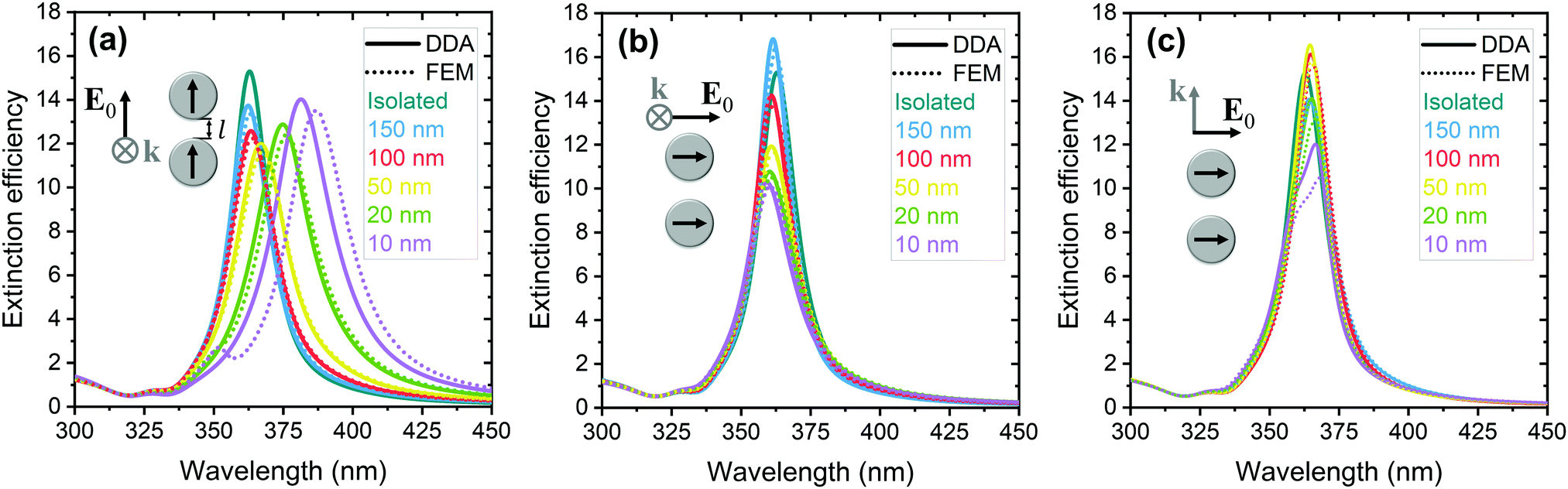 | ||
| Fig. 1 Q ext spectra of 50 nm Ag NP dimers, for different gaps and geometries of incidence, obtained from DDA (solid lines) and FEM (dotted lines) calculations. (a) E0 ‖ and k ⊥ to the alignment axis, (b) E0 and k ⊥ to the alignment axis, and (c) E0 ⊥ and k ‖ to the alignment axis. Qext for an isolated NP (calculated from the Kuwata polarizability) is also included for comparison purposes. | ||
The Qext spectra obtained from DDA and FEM are in good agreement for values of l higher than approximately 20 nm (weak coupling). For smaller gap separations, a lower wavelength multipolar resonance mode appears (at ∼351 nm for l = 10 nm), not described by the single dipole DDA method. This mode, studied in previously published studies,12 is a consequence of the non-uniformity of the field induced in each NP due to the coupling. For even smaller gaps, other higher multipolar modes appear, as the dipole mode shifts continuously towards infinite wavelengths.12 In the single dipole DDA model, the induced field by other NPs in an individual NP is described by the dipole field in its central position. We assume that the dipole field is uniform throughout the region of the space it occupies (quasistatic approximation). In the weak coupling this assumption is valid; however, this model is not capable of describing the strong coupling of NPs, in which the induced dipole field is no longer uniform, and the scattering field also ceases to be described by the field of a dipole. Nevertheless, this model is very useful, as it permits to describe the optical properties of assemblies of NPs in many experimental circumstances, with considerably lower computational times (CPU time differences higher than 4 orders of magnitude between the single dipole DDA method and FEM).
The Qsca and Qabs spectra for 50 nm Ag NP dimers are presented in Fig. S1.2 (ESI†), where it is observed that for 50 nm NPs the absorption and scattering have similar contributions to the extinction.
To better evaluate the validity of the implemented model, Fig. 2 presents the LSPR wavelength and maximum of the dipolar Qext peak of Ag NP dimers, for E0 polarized along the alignment axis, as a function of the gap distance, for four NP sizes (20, 50, 80, and 100 nm). These results were calculated from the single dipole DDA method and compared with FEM simulations for some discrete gap values. For large separations (l ≳ 200 nm), the LSPR wavelength and maximum Qext oscillate around the values of an isolated NP. This behaviour can be explained by the dipole field oscillation in the radiation zone (far-field). For lower separations, they start to increase as the effective incident field increases. Below 100 nm of the NP diameter, the LSPR wavelength from DDA agrees with FEM values for gap values higher than approximately the NP radius. Regarding the maximum Qext, some deviations are also depicted, even for greater gap distances between NPs, despite the identical behaviour.
 | ||
| Fig. 2 Gap-dependence of the far-field LSPR wavelength (a) and maximum (b) of the dipolar Qext peak of Ag NP dimers of different diameters, calculated from DDA (solid lines) and FEM (square symbols), for E0 ‖ and k ⊥ to the alignment axis. | ||
The  of 50 nm Ag NP dimers is represented in Fig. 3 for k perpendicular and E0 parallel (3a) or perpendicular (3b) to the alignment axis calculated from the single dipole DDA method and FEM simulations. The k parallel geometry is not represented as the two NPs have a different near-field spectrum, which depends on the incident field phase. The represented spectra follow the same trend as the far-field Qext. Nevertheless, there is a systematic increase in the maximum
  calculated from FEM in comparison with that calculated from DDA, even for an isolated NP. This difference may be related to the limited mesh size of FEM simulations. The QNF,max and the field magnitude in the gap midpoint, QNF,m, are represented in Fig. S1.3 (ESI†). In these results, the increased near-field for the parallel polarization is more evident as they are calculated in a single point, although in the strong coupling regime the near-field enhancement is even higher.15Fig. 3c and d presents the near-field distribution of the magnitude of the total (scattering + incident) electric field around 50 nm Ag NP dimers of l = 20 nm, calculated from the single dipole DDA method, for the same polarization geometries of Fig. 3a and b, respectively. The fields were obtained at the
  peak wavelength, close to the far-field LSPR peak. The electric field inside NPs was estimated through quasistatic approximation equations (see the ESI†), considering the effective incident electric field. The maximum near-field enhancement occurs in the gap of the dimer for E0 parallel to the alignment axis, as has been reported previously,11,15 contrary to the perpendicular polarization (see Fig. S1.4, ESI† for comparing the field with that of an isolated NP). In addition, Fig. 3c and d shows the scattering dipolar field vectors produced by the left NP in the represented plane, where it is observed how this field is experienced by the right NP. In the weak coupling regime, the induced dipole field from each NP is nearly uniform, but, as the gap distance decreases, that approximation is no longer valid (see Fig. S1.5 and S1.6 (ESI†), with the near-field distributions for 50 nm Ag NP dimers with gaps of 150, 100, 50, and 10 nm from DDA and FEM, respectively), especially when E0 is parallel to the alignment axis (2a). For the perpendicular case (2b), the induced field is nearly uniform even for small gaps, and the validity range of our model is more extensive.
 | ||
Fig. 3 Near-field behaviour of 50 nm Ag NP dimers. (a and b)  spectra for different gaps, obtained from DDA (solid lines) and FEM (dotted lines) calculations. (c and d) Electric field distributions (E/E0) for l = 20 nm, at the spectra for different gaps, obtained from DDA (solid lines) and FEM (dotted lines) calculations. (c and d) Electric field distributions (E/E0) for l = 20 nm, at the  peak wavelength, calculated from DDA. Scattering field vectors of the left NP (inside the right NP the magnitude of the vectors is multiplied by 10). Geometries of incidence: (a and c) E0 ‖ to the alignment axis and (b and d) E0 and k ⊥ to the alignment axis. peak wavelength, calculated from DDA. Scattering field vectors of the left NP (inside the right NP the magnitude of the vectors is multiplied by 10). Geometries of incidence: (a and c) E0 ‖ to the alignment axis and (b and d) E0 and k ⊥ to the alignment axis. | ||
These results for NP dimers show that the single dipole DDA method can be applied to reliably evaluate the far-field and near-field spectra of coupled NPs in the weak coupling regime.
Substrate effect
We start to examine the optical properties of a spherical Ag NP close to a GaN substrate (Kawashima permittivity83). Fig. 4 shows the Qabs and of a 50 nm NP for different gaps between the NP surface and the substrate, considering our DDA modified method and the IDM and FEM simulations. The spectra are represented for different incident geometries. In FEM, a 300 nm thick substrate was considered. Due to the finite dimension of the substrate, for the geometry of E0 and k parallel to the substrate (4c and f), the incident field in the NP is not null, and as a consequence, the efficiencies are also not null, as it would be expected. To compare the DDA modified method with such FEM simulations, a 0.3 multiplication factor, obtained from the FEM simulations, was considered for the amplitude of the incident field in the DDA model. The Qext is not represented here, as numerically it is not possible to accurately separate the scattering component of the NP and substrate; however, the Qext and Qsca spectra calculated from DDA and IDM are represented in Fig. S1.7 (ESI†). The spectral behaviour in terms of the position and maximum of the dipolar peak can be interpreted based on the dimer coupling discussed above. As noted, the presence of the GaN substrate leads to a redshift of the Qabs peak. The electric dipole formed by the NP will induce the accumulation of charges with opposite sign on the substrate in the vicinity of the particle. This polarization of the substrate gives rise to an increase in the damping factor of the system, resulting in a decrease of the resonance frequency. In fact, from eqn (7), it is observed that the resonance condition occurs when the term in parentheses is zero, which, considering the Rayleigh polarizability for comparison, gives
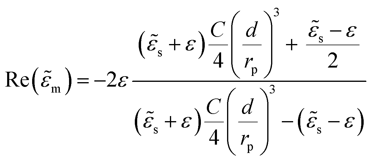 | (14) |
m) ≈ 0. When s = ε or when the distance d between the NP and the substrate tends to infinity, the condition Re(m) = −2ε is obtained, which matches to the resonance condition in the Rayleigh approximation for isolated particles. When s > ε, Re(m) < −2ε comes. Comparing with the Rayleigh condition, the resonance peak redshifts, as for metals Re(m) decreases as the wavelength increases (Drude behaviour). On the other hand, when s < ε, Re(m) > −2ε is obtained, which results in a blueshift of the resonance peak. It is also verified that, for a perpendicular polarization (C = 16), the shift of the resonance peak is greater in relation to the parallel polarization (C = 32). In fact, this is what is observed for the IDM, although, as the coupling between the NP and its image is not considered, it does not describe well the behaviour of the spectra. On the other hand, our model based on DDA is in good agreement with the FEM simulations, mainly for the parallel polarization geometries, with some deviations only for a zero-gap distance. For the perpendicular polarization geometry, the deviations become larger, as in a dimer, due to the non-uniform field induced in the NP. Moreover, the divergences between DDA and FEM simulations increase as the gap distance approaches to zero, particularly evident with many higher order modes arising.12 For k perpendicular and E0 parallel to the substrate surface (4a and d), the splitting of the dipolar Qabs peak for small gaps results from the phase difference between the NP and its image. The decrease of Qabs and  is related to the wave reflected in the substrate, which is in phase opposition to the incident wave, giving rise to a destructive interference close to the substrate. The DDA modified model also better describes the
  compared to the IDM, though, concerning the field distribution, it only permits results in agreement with FEM simulations for gaps higher than approximately 10 nm (see Fig. S1.8, ESI,† with the comparison of the field distributions for a Ag NP close to a GaN substrate, calculated by the DDA modified method and FEM).
 | ||
Fig. 4 (a–c) Qabs and (d–f)  spectra for a 50 nm Ag NP close to a GaN substrate, for different gaps and geometries of incidence, obtained from our DDA method (solid lines), IDM (dashed lines) and FEM (dotted lines) calculations. (a and d) E0 ‖ and k ⊥ to the substrate surface, (b and e) E0 ⊥ and k ‖ to the substrate, and (c and f) E0 ‖ and k ‖ to the substrate. spectra for a 50 nm Ag NP close to a GaN substrate, for different gaps and geometries of incidence, obtained from our DDA method (solid lines), IDM (dashed lines) and FEM (dotted lines) calculations. (a and d) E0 ‖ and k ⊥ to the substrate surface, (b and e) E0 ⊥ and k ‖ to the substrate, and (c and f) E0 ‖ and k ‖ to the substrate. | ||
The Qabs spectra for 20 nm and 80 nm Ag NPs close to a GaN substrate are represented in Fig. S1.9 (ESI†), where our model is always able to better reproduce the FEM results compared to the IDM, even if for the 80 nm Ag NPs the model does not reproduce the quadrupolar modes of higher frequency.
A semiconductor substrate has a non-negligible imaginary permittivity component, which plays an important role in the spectral features of the NPs, as it introduces a phase difference in the scattering field of the NP and its image. Fig. 5 presents the dependence of Qext on the substrate permittivity for a 50 nm Ag NP, for k perpendicular to the substrate surface. As Re(s) increases, a redshift of the resonance peak is observed for small imaginary components. This behaviour is consistent with experimental studies in dielectric substrates.41 With the increase of Im(s), there is a widening and a splitting of the Qext peak due to the phase difference introduced by the Δs term. For higher values of Im(s), Δs tends to 1, and the spectrum approaches that obtained for higher values of Re(s).
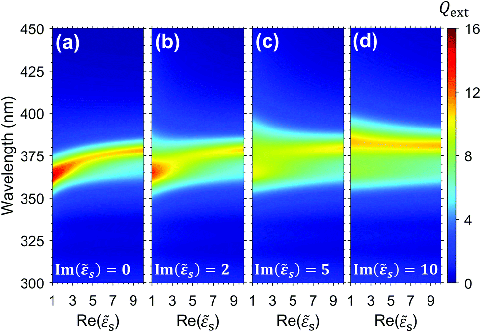 | ||
| Fig. 5 Q ext map for a 50 nm Ag NP on a substrate (zero gap) for k ⊥ to the substrate as a function of the wavelength and the real permittivity of the substrate for different imaginary permittivities: 0, 2, 5, and 10. | ||
Array of NPs on a substrate
Our DDA modified method can also be used to study the response of NP arrays. Fig. 6 compares the Qext of a 10 × 10 square array (6a and c) and a 100 NP random array (6b and d) of 50 nm Ag NPs on a GaN substrate (solid lines) for different interparticle gap distances. The surface densities in the random arrays were chosen in order to be equivalent to the square arrays. The positions of the particles in the random arrays were defined in a pseudo-random way, ensuring a 10 nm minimum gap between NPs. Without this condition, the spectra do not change significantly due to the average behaviour. For a 20 nm gap square array, the surface density is too high to randomly define positions. Due to the position randomness of particles, for each surface density, the average Qext of ten different distributions is represented. The spectra are represented for two incident geometries: k perpendicular to the substrate and E0 parallel to the NP alignment (6a and b), where a zero-gap with the substrate was considered, and E0 perpendicular and k parallel to the NP alignment (6c and d), where a 5 nm gap was considered, to guarantee the model validity. To analyze the impact of the GaN substrate, the efficiencies in the absence of the GaN substrate (dashed lines) are also represented. In Fig. 6a and b, the widening and redshift of the resonance peak observed with the decreased interparticle gap can be interpreted by the overlap of the effects discussed for NP dimers, especially from the interaction of particles along the same axis, in the direction of E0. In Fig. 6c and d, dipoles can only interact laterally, but the phase difference between the NPs in the array explains the observed redshift. Regarding the GaN substrate effect, the main result is the additional redshift of the Qext peak, together with changes in the spectral shape, as shown in Fig. 4. For the square arrays, due to the NP periodicity, an interference phenomenon appears for k parallel to the NP alignment, giving rise to standing modes along the array. As an example, a 436 nm peak can be observed in Fig. 6c for a 500 nm gap. This phenomenon would be even more clear for larger arrays. The existence of standing modes has a practical impact on the usage of the plasmonic phenomena, e.g., due to the attenuation of LSPR modes as a result of destructive interference, as in the 390 nm destructive interference observed in Fig. 6c for a 150 nm gap. The interference also results in a non-monotonic variation of the Qext peak maximum for the square arrays with the increase in surface density, especially for large gap separations, due to the far-field dipole field oscillations. For the random arrays, the interference peaks disappear, and a gradual decrease of the peak maximum is observed with the increase in surface density, but the randomness of the NPs appears to not change the position of the resonance peaks. | ||
| Fig. 6 Q ext spectra for a (a and c) square and a (b and d) random array of 100 Ag NPs of 50 nm size close to a GaN substrate ((a and b) 0 nm gap and (c and d) 5 nm gap), and without the substrate effect, for different interparticle gaps and surface densities. Geometries of incidence: (a and b) k ⊥ to the substrate surface and (c and d) E0 ⊥ to the substrate. | ||
The Qsca and Qabs spectra for the same square and random arrays are represented in Fig. S1.10 (ESI†), where a decrease of Qabs relative to Qsca is observed in comparison with the isolated NP.
Conclusions
We developed a semi-analytical procedure based on DDA to simulate the far-field and near-field properties of arrays of NPs, considering the weak coupling between particles and the effect of the presence of a substrate, based on the image dipole approach. In the presented calculations, a single dipole model was considered, in which the polarizability is calculated using the empirical formula of Kuwata. This model has the great advantage of allowing very quick calculations for large arrays of NPs, unlike numerical approaches.The method was first tested for dimers of Ag NPs and single Ag NPs on a gallium nitride (GaN) substrate for different incident field geometries, indicating a good agreement with FEM simulations in the weak coupling regime. Then, we presented the optical properties of 2D square and random arrays of Ag NPs on a GaN substrate. It was found that the increased surface density and the GaN substrate mainly result in a redshift and a widening of the dipolar resonance of the NPs, and an increase in the near-field enhancement in the gap regions. The randomness in the distribution of the NPs mainly results in an extinction of the standing modes of the square arrays and a monotonic variation of the efficiencies with the surface density.
The presented results give new insights into the weak coupling between NPs and a semiconductor substrate. Furthermore, the described model provides a new tool to predict the optical properties of large arrays of NPs on a semiconductor or a dielectric substrate, in order to develop optimized optical structures for many technological domains.
Author contributions
Diogo F. Carvalho: conceptualization, methodology, software, validation, writing – original draft, writing – review & editing. Manuel A. Martins: supervision, writing – review & editing. Paulo A. Fernandes: supervision, writing – review & editing. M. Rosário P. Correia: conceptualization, methodology, supervision, validation, writing – original draft, writing – review & editing.Conflicts of interest
There are no conflicts to declare.Acknowledgements
This work was partially developed within the scope of the projects i3N, UIDB/50025/2020 (BI/UI96/9549/2021 grant) & UIDP/50025/2020, and CICECO-Aveiro Institute of Materials, UIDB/50011/2020, UIDP/50011/2020 & LA/P/0006/2020, financed by national funds through the FCT/MEC. This research was also funded in part by the 2021.08228.BD FCT grant.Notes and references
- H. A. Atwater and A. Polman, Materials for Sustainable Energy, Co-Published with Macmillan Publishers Ltd, UK, 2010, vol. 2, pp. 1–11 Search PubMed.
- Y.-F. Li, Z.-L. Kou, J. Feng and H.-B. Sun, Nanophotonics, 2020, 9, 3111–3133 CrossRef CAS.
- K. Okamoto, M. Funato, Y. Kawakami and K. Tamada, J. Photochem. Photobiol., C, 2017, 32, 58–77 CrossRef CAS.
- S. Szunerits and R. Boukherroub, Chem. Commun., 2012, 48, 8999 RSC.
- Y. Peng, B. Xiong, L. Peng, H. Li, Y. He and E. S. Yeung, Anal. Chem., 2015, 87, 200–215 CrossRef CAS PubMed.
- A. Wang and X. Kong, Materials, 2015, 8, 3024–3052 CrossRef CAS PubMed.
- V. Shvalya, G. Filipič, J. Zavašnik, I. Abdulhalim and U. Cvelbar, Appl. Phys. Rev., 2020, 7, 031307 CAS.
- K. L. Kelly, E. Coronado, L. L. Zhao and G. C. Schatz, J. Phys. Chem. B, 2003, 107, 668–677 CrossRef CAS.
- M. Schmid, P. Andrae and P. Manley, Nanoscale Res. Lett., 2014, 9, 1–11 CrossRef PubMed.
- W. Rechberger, A. Hohenau, A. Leitner, J. R. Krenn, B. Lamprecht and F. R. Aussenegg, Opt. Commun., 2003, 220, 137–141 CrossRef CAS.
- E. Hao and G. C. Schatz, J. Chem. Phys., 2004, 120, 357–366 CrossRef CAS PubMed.
- I. Romero, J. Aizpurua, G. W. Bryant and F. J. García De Abajo, Opt. Express, 2006, 14, 9988 CrossRef PubMed.
- P. K. Jain, W. Huang and M. A. El-Sayed, Nano Lett., 2007, 7, 2080–2088 CrossRef CAS.
- A. M. Funston, C. Novo, T. J. Davis and P. Mulvaney, Nano Lett., 2009, 9, 1651–1658 CrossRef CAS PubMed.
- Y. Huang, Q. Zhou, M. Hou, L. Ma and Z. Zhang, Phys. Chem. Chem. Phys., 2015, 17, 29293–29298 RSC.
- Y. Wang, J. W. Barr, S. Gomrok, E. Chaffin and X. Huang, J. Phys. Chem. C, 2021, 125, 5260–5268 CrossRef PubMed.
- Y. Yokota, K. Ueno and H. Misawa, Chem. Commun., 2011, 47, 3505 RSC.
- J. Ye, F. Wen, H. Sobhani, J. B. Lassiter, P. van Dorpe, P. Nordlander and N. J. Halas, Nano Lett., 2012, 12, 1660–1667 CrossRef CAS PubMed.
- N. Pazos-Perez, C. S. Wagner, J. M. Romo-Herrera, L. M. Liz-Marzán, F. J. García de Abajo, A. Wittemann, A. Fery and R. A. Alvarez-Puebla, Angew. Chem., Int. Ed., 2012, 51, 12688–12693 CrossRef CAS PubMed.
- S. Dutta Roy, M. Ghosh and J. Chowdhury, J. Phys. Chem. C, 2018, 122, 10981–10991 CrossRef CAS.
- C. F. Bohren and D. R. Huffman, Absorption and Scattering of Light by Small Particles, Wiley, 1998 Search PubMed.
- J. Aizpurua, G. W. Bryant, L. J. Richter, F. J. García de Abajo, B. K. Kelley and T. Mallouk, Phys. Rev. B: Condens. Matter Mater. Phys., 2005, 71, 235420 CrossRef.
- D. W. Mackowski, J. Opt. Soc. Am. A, 1994, 11, 2851 CrossRef.
- L. Zhao, K. L. Kelly and G. C. Schatz, J. Phys. Chem. B, 2003, 107, 7343–7350 CrossRef CAS.
- N. Harris, M. D. Arnold, M. G. Blaber and M. J. Ford, J. Phys. Chem. C, 2009, 113, 2784–2791 CrossRef CAS.
- A. I. Dolinnyi, J. Phys. Chem. C, 2015, 119, 4990–5001 CrossRef CAS.
- B. T. Draine and P. J. Flatau, J. Opt. Soc. Am. A, 1994, 11, 1491–1499 CrossRef.
- W. H. Yang, G. C. Schatz and R. P. van Duyne, J. Chem. Phys., 1995, 103, 869–875 CrossRef CAS.
- V. Amendola, O. M. Bakr and F. Stellacci, Plasmonics, 2010, 5, 85–97 CrossRef CAS.
- A. Taflove and S. C. Hagness, Computational electrodynamics: the finite-difference time-domain method, Artech House, 2005 Search PubMed.
- C. E. Talley, J. B. Jackson, C. Oubre, N. K. Grady, C. W. Hollars, S. M. Lane, T. R. Huser, P. Nordlander and N. J. Halas, Nano Lett., 2005, 5, 1569–1574 CrossRef CAS PubMed.
- Y. Chu, E. Schonbrun, T. Yang and K. B. Crozier, Appl. Phys. Lett., 2008, 93, 181108 CrossRef.
- L. v Brown, H. Sobhani, J. B. Lassiter, P. Nordlander and N. J. Halas, ACS Nano, 2010, 4, 819–832 CrossRef CAS PubMed.
- X. Lin, S. Lin, Y. Liu, H. Zhao, L. Wang and W. Hasi, Plasmonics, 2018, 13, 1749–1758 CrossRef CAS.
- J.-M. Jin, The Finite Element Method in Electromagnetics, Wiley-IEEE Press, 2014 Search PubMed.
- Z. B. Wang, B. S. Luk’yanchuk, W. Guo, S. P. Edwardson, D. J. Whitehead, L. Li, Z. Liu and K. G. Watkins, J. Chem. Phys., 2008, 128, 094705 CrossRef CAS PubMed.
- J. M. McMahon, A. I. Henry, K. L. Wustholz, M. J. Natan, R. G. Freeman, R. P. van Duyne and G. C. Schatz, Anal. Bioanal. Chem., 2009, 394, 1819–1825 CrossRef CAS PubMed.
- C. P. Burrows and W. L. Barnes, Opt. Express, 2010, 18, 3187 CrossRef CAS PubMed.
- K. L. Wustholz, A. I. Henry, J. M. McMahon, R. G. Freeman, N. Valley, M. E. Piotti, M. J. Natan, G. C. Schatz and R. P. V. Duyne, J. Am. Chem. Soc., 2010, 132, 10903–10910 CrossRef CAS PubMed.
- F. Le, D. W. Brandl, Y. A. Urzhumov, H. Wang, J. Kundu, N. J. Halas, J. Aizpurua and P. Nordlander, ACS Nano, 2008, 2, 707–718 CrossRef CAS PubMed.
- M. W. Knight, Y. Wu, J. B. Lassiter, P. Nordlander and N. J. Halas, Nano Lett., 2009, 9, 2188–2192 CrossRef CAS PubMed.
- Y. Wu and P. Nordlander, J. Phys. Chem. C, 2010, 114, 7302–7307 CrossRef CAS.
- P. Spinelli, C. van Lare, E. Verhagen and A. Polman, Opt. Express, 2011, 19, A303 CrossRef PubMed.
- T. Hutter, S. R. Elliott and S. Mahajan, Nanotechnology, 2013, 24, 035201 CrossRef PubMed.
- R. T. Hill, J. J. Mock, Y. Urzhumov, D. S. Sebba, S. J. Oldenburg, S. Y. Chen, A. A. Lazarides, A. Chilkoti and D. R. Smith, Nano Lett., 2010, 10, 4150–4154 CrossRef CAS PubMed.
- S.-Y. Ding, J. Yi, J.-F. Li, B. Ren, D.-Y. Wu, R. Panneerselvam and Z.-Q. Tian, Nat. Rev. Mater., 2016, 1, 16021 CrossRef CAS.
- G.-C. Li, Y.-L. Zhang and D. Y. Lei, Nanoscale, 2016, 8, 7119–7126 RSC.
- V. Devaraj, J.-M. Lee and J.-W. Oh, Nanomaterials, 2018, 8, 582 CrossRef PubMed.
- T. Yamaguchi, S. Yoshida and A. Kinbara, Thin Solid Films, 1974, 21, 173–187 CrossRef CAS.
- A. Pinchuk, A. Hilger, G. von Plessen and U. Kreibig, Nanotechnology, 2004, 15, 1890–1896 CrossRef CAS.
- V. Myroshnychenko, J. Rodríguez-Fernández, I. Pastoriza-Santos, A. M. Funston, C. Novo, P. Mulvaney, L. M. Liz-Marzán and F. J. García de Abajo, Chem. Soc. Rev., 2008, 37, 1792–1805 RSC.
- K. C. Vernon, A. M. Funston, C. Novo, D. E. Gómez, P. Mulvaney and T. J. Davis, Nano Lett., 2010, 10, 2080–2086 CrossRef CAS PubMed.
- M. M. Wind, J. Vlieger and D. Bedeaux, Phys. A, 1987, 141, 33–57 CrossRef.
- V. v Gozhenko, L. G. Grechko and K. W. Whites, Phys. Rev. B: Condens. Matter Mater. Phys., 2003, 68, 125422 CrossRef.
- B. T. Draine, Astrophys. J., 1988, 333, 848 CrossRef CAS.
- B. T. Draine and J. Goodman, Astrophys. J., 1993, 405, 685 CrossRef.
- K. Svoboda and S. M. Block, Opt. Lett., 1994, 19, 930 CrossRef CAS PubMed.
- W. Liu and E. McLeod, J. Phys. Chem. C, 2019, 123, 13009–13014 CrossRef CAS.
- H. Kuwata, H. Tamaru, K. Esumi and K. Miyano, Appl. Phys. Lett., 2003, 83, 4625–4627 CrossRef CAS.
- M. Meier and A. Wokaun, Opt. Lett., 1983, 8, 581 CrossRef CAS PubMed.
- A. Melikyan and H. Minassian, Appl. Phys. B: Lasers Opt., 2004, 78, 453–455 CrossRef CAS.
- M. K. Kinnan and G. Chumanov, J. Phys. Chem. C, 2010, 114, 7496–7501 CrossRef CAS.
- J. Lin, A. Llopis, A. Krokhin, S. Pereira, I. M. Watson and A. Neogi, Appl. Phys. Lett., 2014, 104, 1–5 Search PubMed.
- S. Pillai, K. R. Catchpole, T. Trupke and M. A. Green, J. Appl. Phys., 2007, 101, 093105 CrossRef.
- C.-Y. Cho, M.-K. Kwon, S.-J. Lee, S.-H. Han, J.-W. Kang, S.-E. Kang, D.-Y. Lee and S.-J. Park, Nanotechnology, 2010, 21, 205201 CrossRef PubMed.
- J. Tatebayashi, T. Yamada, T. Inaba, S. Ichikawa and Y. Fujiwara, Jpn. J. Appl. Phys., 2019, 58, SCCC09 CrossRef CAS.
- G. Y. Mak, W. Y. Fu, E. Y. Lam and H. W. Choi, Phys. Status Solidi C, 2009, 6, S654–S657 Search PubMed.
- P. Viste, J. Plain, R. Jaffiol, A. Vial, P. M. Adam and P. Royer, ACS Nano, 2010, 4, 759–764 CrossRef CAS PubMed.
- A. G. Nikitin, T. Nguyen and H. Dallaporta, Appl. Phys. Lett., 2013, 102, 221116 CrossRef.
- N. Gisbert Quilis, M. Lequeux, P. Venugopalan, I. Khan, W. Knoll, S. Boujday, M. Lamy de la Chapelle and J. Dostalek, Nanoscale, 2018, 10, 10268–10276 RSC.
- Y. Chen, K. J. Si, D. Sikdar, Y. Tang, M. Premaratne and W. Cheng, Adv. Opt. Mater., 2015, 3, 919–924 CrossRef CAS.
- S. Lin, X. Lin, Y. Shang, S. Han, W. Hasi and L. Wang, J. Phys. Chem. C, 2019, 123, 24714–24722 CrossRef CAS.
- B. Auguié and W. L. Barnes, Opt. Lett., 2009, 34, 401 CrossRef PubMed.
- S. Bakhti, A. v Tishchenko, X. Zambrana-Puyalto, N. Bonod, S. D. Dhuey, P. J. Schuck, S. Cabrini, S. Alayoglu and N. Destouches, Sci. Rep., 2016, 6, 32061 CrossRef CAS PubMed.
- M.-K. Kwon, J.-Y. Kim, B.-H. Kim, I.-K. Park, C.-Y. Cho, C. C. Byeon and S.-J. Park, Adv. Mater., 2008, 20, 1253–1257 CrossRef CAS.
- J. Henson, J. C. Heckel, E. Dimakis, J. Abell, A. Bhattacharyya, G. Chumanov, T. D. Moustakas and R. Paiella, Appl. Phys. Lett., 2009, 95, 1–3 CrossRef.
- B. Nie, B. K. Duan and P. W. Bohn, J. Raman Spectrosc., 2012, 43, 1347–1353 CrossRef CAS.
- S. Siddhanta, V. Thakur, C. Narayana and S. M. Shivaprasad, ACS Appl. Mater. Interfaces, 2012, 4, 5807–5812 CrossRef CAS PubMed.
- F.-X. Deng, Y. Zhao, L.-F. Hu, T. Xu, Y.-Q. Liu and G.-B. Pan, RSC Adv., 2014, 4, 42240–42243 RSC.
- K. H. Lee, H. Jang, Y. S. Kim, C. Lee, S. H. Cho, M. Kim, H. Son, K. bin Bae, D. van Dao, Y. S. Jung and I. Lee, Adv. Sci., 2021, 8, 2100640 CrossRef CAS PubMed.
- P. Johnson and R. Christy, Phys. Rev. B: Solid State, 1972, 6, 4370–4379 CrossRef CAS.
- H. J. Pain, The Physics of Vibrations and Waves, Wiley, Chichester, 2005 Search PubMed.
- T. Kawashima, H. Yoshikawa, S. Adachi, S. Fuke and K. Ohtsuka, J. Appl. Phys., 1997, 82, 3528–3535 CrossRef CAS.
Footnote |
| † Electronic supplementary information (ESI) available. See DOI: https://doi.org/10.1039/d2cp02446b |
| This journal is © the Owner Societies 2022 |