
 Open Access Article
 This Open Access Article is licensed under a Creative Commons Attribution-Non Commercial 3.0 Unported Licence
Critical problems faced in Raman-based energy transport characterization of nanomaterials
Ridong
Wang†
a,
Nicholas
Hunter†
b,
Hamidreza
Zobeiri†
b,
Shen
Xu†
c and
Xinwei
Wang
 *b
*b
aState Key Laboratory of Precision Measuring Technology and Instruments, Tianjin University, Tianjin 300072, P. R. China
bDepartment of Mechanical Engineering, Iowa State University, 271 ASC II, 1915 Scholl Road, Ames, IA 50011, USA. E-mail: xwang3@iastate.edu
cSchool of Mechanical and Automotive Engineering, Shanghai University of Engineering Science, Shanghai 201620, P. R. China
First published on 27th July 2022
Abstract
In the last two decades, tremendous research has been conducted on the discovery, design and synthesis, characterization, and applications of two-dimensional (2D) materials. Thermal conductivity and interface thermal conductance/resistance of 2D materials are two critical properties in their applications. Raman spectroscopy, which measures the inelastic scattering of photons by optical phonons, can distinct a 2D material's temperature from its surrounding materials', featuring unprecedented spatial resolution (down to the atomic level). Raman-based thermometry has been used tremendously for characterizing the thermal conductivity of 2D materials (suspended or supported) and interface thermal conductance/resistance. Very large data deviations have been observed in literature, partly due to physical phenomena and factors not considered in measurements. Here, we provide a critical review, analysis, and perspectives about a broad spectrum of physical problems faced in Raman-based thermal characterization of 2D materials, namely interface separation, localized stress due to thermal expansion mismatch, optical interference, conjugated phonon, and hot carrier transport, optical–acoustic phonon thermal nonequilibrium, and radiative electron–hole recombination in monolayer 2D materials. Neglect of these problems will lead to a physically unreasonable understanding of phonon transport and interface energy coupling. In-depth discussions are also provided on the energy transport state-resolved Raman (ET-Raman) technique to overcome these problems and on future research challenges and needs.
1. Introduction
Since the discovery of graphene,1 tremendous research has been conducted on the synthesis, structural characterization and understanding, properties characterization and tailoring, and applications of two-dimensional (2D) materials far beyond graphene.2–8 Thermal conductivity and interface thermal conductance/resistance of 2D materials are two critical properties in their applications such as integrated circuits, energy conversion, photon sensing, and chemical sensing. Because of their extremely small thickness (≤nm), measurement of these two properties faces big challenges, which makes traditional techniques not feasible or suffer very large uncertaintes. Raman spectroscopy, which measures the inelastic scattering of photons by optical phonons, can distinct a 2D material's temperature from its surrounding materials', featuring unprecedented spatial resolution (down to the atomic level).2 Over more than two decades, Raman-based thermometry has been used tremendously in characterizing the thermal conductivity of 2D materials (suspended or supported) and interface thermal conductance/resistance.However, very large data deviations have been reported on the measured thermal conductivity and interface thermal conductance/resistance of 2D materials.9,10 Such deviations can reach the level of orders of magnitude. The deviations can be due to unknown structural differences (impurities, defects, and boundaries/sizes) between samples, that is, the quality of the sample. In addition, a large number of deviations arise because of the measurement factors that have not been taken into consideration in data processing and complicated physical phenomena that are tangled with phonon transport, such as laser absorption coefficient determination, Raman temperature coefficient calibration, and the thermal nonequilibrium among different hot carriers.7,11,12 For instance, the refractive index, which is used to determine the laser absorption coefficient, was determined as around 3.05 and 5.2 for MoS2 by using spectroscopic ellipsometry and a spatially resolved spectrum system, respectively.13,14 The Raman temperature coefficient calibration, which was quite time-consuming, also could introduce a possible error of 25%.9 Moreover, it was found that ignoring the thermal nonequilibrium among different energy carriers can underpredict the thermal conductivity by more than 40%.15 In summary, the deviation of orders of magnitude originates from the combined effects of the above factors, and it is of great importance to analyze these effects thoroughly. This work provides a critical review, analysis, and perspectives about a broad spectrum of physical problems faced during Raman-based thermal characterization of 2D materials. Neglecting these problems will lead to a severe physically unreasonable understanding of phonon transport and interface energy coupling of the 2D materials.
2. Evaluation of photon absorption: optical interference effect
In traditional steady-state Raman-based thermal conductivity and interface thermal resistance measurement of 2D materials, the laser absorption in the 2D material and its temperature rise needs to be quantitatively evaluated. The temperature determination requires a Raman temperature coefficient calibration in a separate experiment. The laser beam absorption is calculated either using optical properties of the 2D material and substrates or by direct measurement. For supported 2D films in the previous Raman study, a perfect contact was usually assumed between the 2D films and their substrates. However, recent works have revealed that an air gap may exist at the interface in most situations, especially, when the supported 2D film is prepared using mechanical exfoliation and physical transferring methods.16,17 This air gap will introduce an additional layer in the sample structure as shown in Fig. 1. The incident laser rays are reflected from the bottom of the 2D layer and the top of the substrate. Then, the reflections interfere with other reflections to introduce an interference effect and alter the local laser intensity in the 2D film. It can cause considerable change in the optical absorption of the 2D film.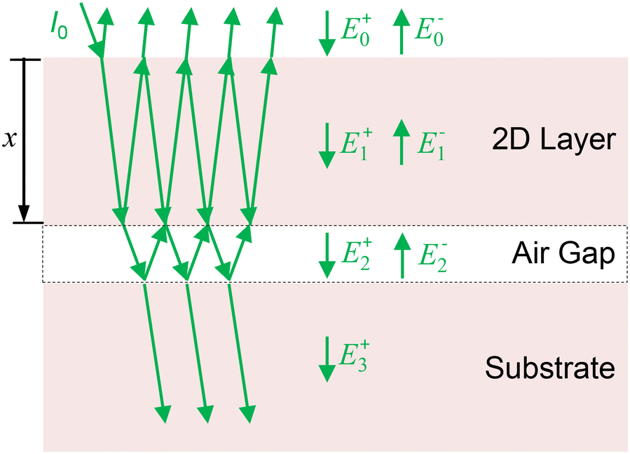 | ||
| Fig. 1 Schematic of the incident laser reflections and refractions in a multilayer structure. | ||
Considering the interference effect induced by the air gap, the absorbed electrical field E1(x) in the supported 2D film has an expression as:
| E1(x) = (D1,11/S1,11e−iβ1(d1−x)) + D1,21/S1,11e−iβ1(d1−x))E0+, | (1) |
The effect of the air gap on the laser absorption in the supported 2D film is investigated here for two supported MoS2 samples. Sample #1 is a MoS2 film on a silicon (Si) substrate and sample #2 is a MoS2 film on a glass (SiO2) substrate. The thicknesses of the MoS2 film and the air gap are varied in the calculation to explore the interference effect on the laser absorption. The refractive index of each material is listed in Table 1, and the calculated absorption is shown in Fig. 2. In Fig. 2(a), for the four supported 2D material cases (monolayer, bi-layer, 5-layer, and 10-layer MoS2 films), the absorption is first enhanced and then reduced when the thickness of the air gap increases. The enhancement factor is defined as (A − A0)/A0, where A is the absorption of the MoS2 film,  , A0 is the absorption of the supported film without air gap, and τL is the laser absorption depth. Along with the increase in the layer number of the MoS2 film, A0 becomes large, and the reflected beam at the MoS2 surface (top and bottom) becomes weaker, making the interference effect weaker. Therefore, the enhancement factor (the ratio) will be lower for thicker films, as shown in Fig. 2(a).
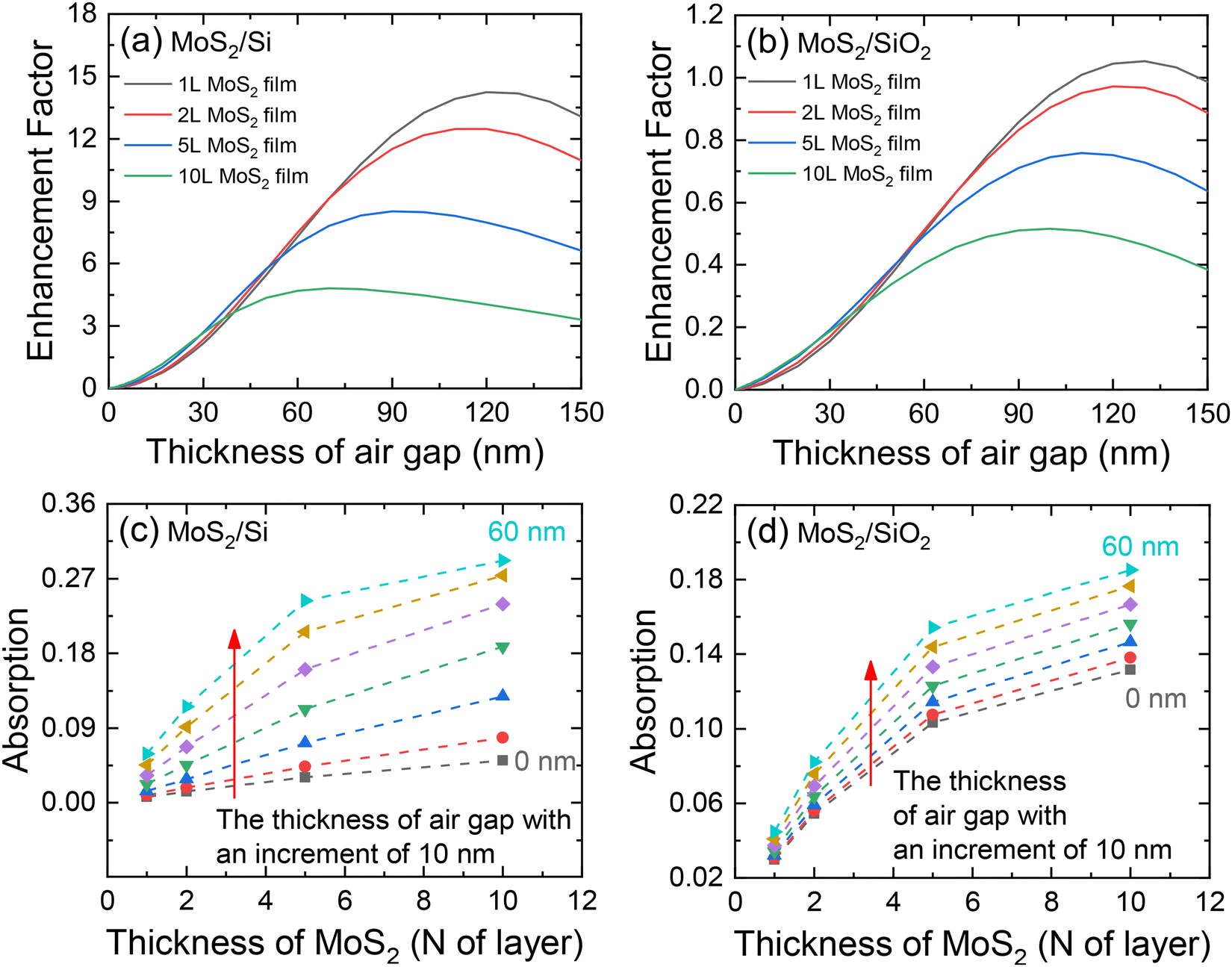 | ||
| Fig. 2 Laser absorption in supported MoS2 films. Absorption enhancement factor in the MoS2 layer of (a) MoS2/Si sample and (b) MoS2/SiO2 sample against the air gap thickness. Absolute laser absorption in the MoS2 layer of (c) MoS2/Si sample and (d) MoS2/SiO2 sample against MoS2 thickness. | ||
However, an air gap thicker than ∼100 nm is less observed in supported film structures. For sample #1, the assessment in the next section demonstrates the air gap can be as large as 37 nm. The occurrence of boundary slip will decrease the gap thickness. The enhancement factor is reasonably regarded as monotonically increasing against the air gap thickness before the air gap reaches 37 nm thick. When the air gap reaches 37 nm, as mentioned above, the absorption enhancement factor can be 3.20∼3.40. This means that strong reflections occur on the top surface of the Si substrate due to its large refractive index (ñ3 = 4.1506 + 0.0516i) at 532 nm. The reflected rays go backward into the 2D layer, interfere with the rays remaining in the 2D layer, and enhance the local laser intensity as well as the absorption. In comparison with sample #1, the SiO2 substrate in sample #2 has a very different refractive index  . Weak reflections occur on the top of the substrate, and thus the interference effect and absorption enhancement factor in the 2D film are much lower, as shown in Fig. 2(b). In the whole range of the studied air gap thickness (0–160 nm), the maximum enhancement factor is less than 1.1 and much less than that of sample #1. For a more commonly used structure in the real case that a silicon substrate has a thin native oxide layer, the thin oxide layer will introduce an additional oscillation in the absorbed incident laser intensity in the sample layer. Together with the silicon substrate, both oscillations contribute to the interference effect on the sample's laser energy absorption and render the intensity enhancement more complicated.
Besides the air-gap-induced interference effect, the thickness of the 2D film also affects the absorption of the laser by it. When combined with the interference effect, the enhancement becomes more significant. As no air gap exists in sample #1, the absorption in the MoS2 film increases against the layer number of MoS2, as shown in black in Fig. 2(c). The absorption in this case increases from 0.0071 to 0.0091, when the layer number changes from 1 to 10. The thickness of a single MoS2 layer is about 0.615 nm.22 However, the increasing rates of the multilayered MoS2 cases with an air gap are much faster than those without the air gap. Taking the case with the 60 nm thick air gap as an example [the light blue dash line in Fig. 2(c)], its absorption is 0.0589 for the monolayer MoS2 film and 0.292 for the 10-layer MoS2 film. Both of them are significantly higher than the original absorption when there is no air gap. However, for MoS2 on SiO2, as shown in Fig. 2(d), the difference in the increasing trend for the absorption against the layer number is less. SiO2 has large transmittance and weak reflectance, and thus the interference in the MoS2 layer is weak, which manifests that most incident photon energy can penetrate the glass substrate, and little is absorbed by the 2D film. Therefore, the absorption enhancement in the supported MoS2 layer is a combined result of the thickness variation in both the air gap and the MoS2 layer.
The intensity of characteristic Raman peaks generated in the 2D film is proportional to the local laser intensity, thus it should be sensitive to the interface air gap. Tang et al.16,17 investigated the air gap thickness between few-layered graphene and the substrate under different heating conditions, such as laser-heating from sample top and pad-heating from sample bottom. The investigation revealed that the interface spacing of the supported 2D film sample in Raman-based thermal measurement is different from that in Raman temperature coefficient calibration due to different interfacial thermal expansion mismatch. Yuan et al.7,23 measured the interface thermal conductance and hot carrier diffusion coefficient in 2D semiconductors based on the accurate evaluation of laser absorption in the layer. In addition to local intensity, the location where the scattering is excited in the layer is also important. It introduces an additional source term in the transfer matrix. The specific location where a certain beam of the Raman scatterings emerges will affect the interference effect on the intensity of the finally gathered Raman signal, which is termed as “non-continuity of the Raman signal”. An early multilayer model was built to evaluate the interference effect without considering the non-continuity of Raman scattering.24 Velson et al.18 developed a physical model for rigorous calculation of the Raman intensity from a multilayer film system based on the transfer matrix method including the effects from both the air gap and non-continuity of Raman generation. Suspended 2D films have no air gap and the substrate, however, the interference effect raised by the film thickness still exists and affects the local absorption of the incident laser. When the incident beams are reflected on the top and bottom surfaces, the reflections will interfere with and alter the local laser intensity in the suspended film. In thermal characterization experiments, unknown optical properties of the emerging 2D materials will raise large difficulty in accurate determination of laser absorption.
One efficient way to eliminate the effect of unknown absorption in various 2D materials is using transient methods, such as frequency-domain energy transport state-resolved Raman (FET-Raman).25 The FET-Raman employs an amplitude-modulated excitation laser (a duty cycle of 50%) to heat up the sample and measure the Raman scattering at the same time. The Raman shift power coefficient (RSC: ψf = ∂ω/∂P) is measured. Also ψCW under continuous wave (CW) laser heating is measured. Although ψf and ψCW are dependent on the laser beam absorption, thermophysical properties and Raman wave number temperature coefficient, their ratio Θ = ψf/ψCW is independent of the laser beam absorption and Raman wave number temperature coefficient, and can be used to directly determine the sample's thermal conductivity. This idea is similar to the energy transport state-resolved Raman (ET-Raman), which is discussed in Section 7.
3. Localized stress and thermal expansion mismatch
In addition to laser absorption, the temperature effects on the Raman modes of 2D materials should also been explored.26,27 Most researchers reported that the peak positions varied linearly with the increase of temperature within a moderate temperature range. While some studies demonstrated that the temperature dependence of Raman peak positions for transition metal dichalcogenides (TMDs) should be fitted nonlinearly, such as the two Raman modes of the monolayer MoS2 shown in Fig. 3.28–30 Considering the different temperature dependences of Raman modes, thermal strain and thermal expansion coefficient (TEC) mismatch between the substrate and 2D materials should be taken into consideration. Here, both mechanically-exfoliated MoS2 and chemical vapor deposition (CVD) grown MoS2 are taken as examples to explain the effect of TEC mismatch and strain.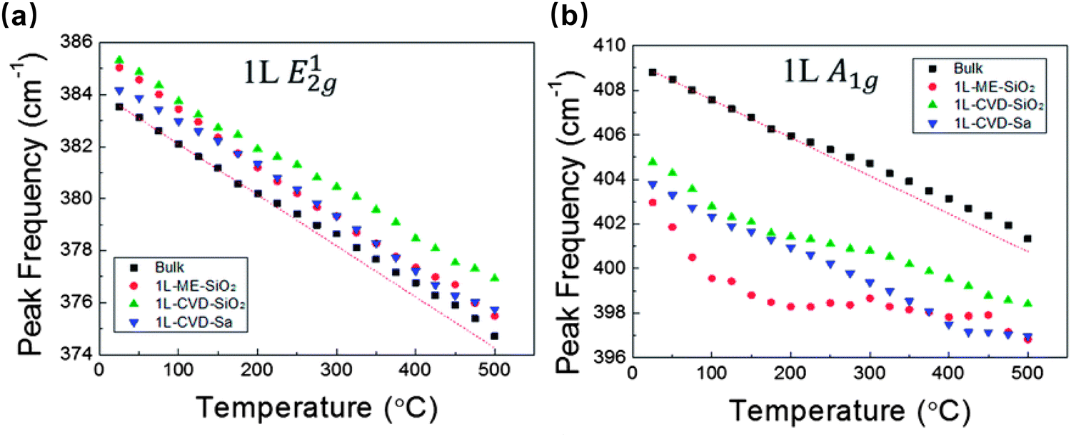 | ||
| Fig. 3 Temperature dependence of the two Raman modes of monolayer MoS2: (a) E2g1 and (b) A1g. Reproduced from ref. 30 with permission from the Royal Society of Chemistry, copyright 2014. | ||
3.1 Supported mechanical exfoliated MoS2 films
In this part, mechanically-exfoliated MoS2 films on the SiO2/Si substrate are used in the discussion. At room temperature (RT), there is one order of magnitude difference in the TECs (α) of SiO2 (0.6 × 10⁻⁶ K−1) and MoS2 (6 × 10⁻⁶ K−1).31 In Raman-based experiments, a typical temperature rise (ΔT) for MoS2 can be assumed to be about 50 K under the laser irradiation area, and a laser spot radius (r0) of 1.5 μm is taken for analysis here. As for the SiO2 substrate, one can safely assume that the thermal expansion takes place only in the MoS2 layer with laser heating because of no heat absorption by the substrate, much lower temperature rise, and very small TEC. Then, equation Δl = 2r0·α·ΔT is employed to calculate the thermal expansion length of the sample, which is 0.9 nm for MoS2. For mechanically transferred MoS2 on SiO2/Si, there is only loose van der Waals force between MoS2 and the substrate. It has very limited constraint on the MoS2 film movement.16 This indicates that the MoS2 films are more likely to be affected by the changes in the film morphology such as wrinkles and ripples when temperature increases. Thus, under laser heating, the TEC mismatch will induce little stress in the MoS2 film. As shown in Fig. 4, an air gap between MoS2 and the substrate is generated, which will cause enhanced charge injection from the substrate into the MoS2 film and decomposition of the absorbed contaminants. To simplify the calculation, an isosceles triangle is utilized, the maximum distance of the air gap is about 37 nm, which is comparable to or higher than the thickness of the MoS2 film. As a result, it is crucial to consider the TEC mismatch in the Raman-based methods. Note in real situations, the pop-up film will have a curve, which can accommodate more of its thermal expansion. Therefore, its real separation from the substrate will be less than the one estimated here.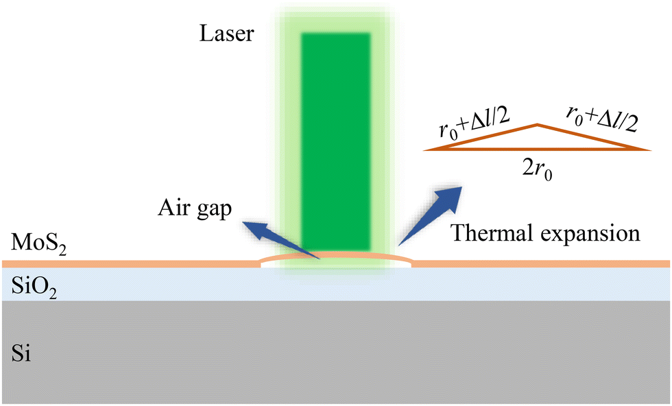 | ||
| Fig. 4 Thermal expansion of the MoS2 film on the SiO2 substrate under laser irradiation. | ||
To further explain the substrate effect, Lin et al.29 studied the temperature-dependent evolutions of both suspended MoS2 and supported MoS2 on the SiO2 substrate. As suspended MoS2 is free of the substrate effect, the Raman shift only originates from lattice expansion. Therefore, it is found the temperature-dependent evolutions are very different. Moreover, compared with the suspended MoS2, the Raman peak positions of supported MoS2 are blue shifted at the same temperature, which reflects the compression of crystalline lattice in supported MoS2 caused by the TEC mismatch between the SiO2 substrate and MoS2. That is, the temperature-dependent Raman shift [ΔωMoS2(T)] of the supported MoS2 are attributed to the thermal expansion of lattice [ΔωE(T)], the anharmonic effect [ΔωA(T)], and strains [ΔωS(T)] induced by the TEC mismatch between the substrate and MoS2. ΔωMoS2(T) can be written as ΔωMoS2(T) = ΔωE(T) + ΔωA(T) + ΔωS(T), and ΔωS(T) can be expressed as  , where β is the biaxial strain coefficient of the Raman mode.29
3.2 Supported CVD grown MoS2 films
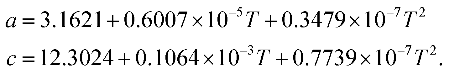
Compared to the mechanically transferred MoS2 on a substrate, the CVD growth of MoS2 films at a temperature higher than 700 °C can lead to stronger chemical bonding between the MoS2 film and substrate.30 Thus, the effect of TEC mismatch on the interface spacing is much smaller here. However, the growth-induced strain and laser heating induced strain should be taken into account in an experiment.17Typically, the growth temperature is 750 °C. At RT, a hexagonal unit cell has dimensions of a = 3.1622 ± 0.007, c = 12.301 ± 0.002 Å for MoS2. The temperature dependence of a and c are:32
 | (2) |
 | (3) |
The other strain is the laser heating induced strain, which is a compressive strain developed because of the increase in the thermal mismatch between MoS2 and the SiO2 substrate. As the A1g and E2g1 modes correspond to the vibration in the z axis and the xy plane, the developed strain is assumed as the biaxial compressive strain. Moreover, the laser induced heat flows radially from the irradiation point. As a result, the hardening of phonon modes may be expected because of compressive strain. In this case, the anharmonic effects caused by laser heating are compensated by the in-plane biaxial compressive strain developed with the laser power because of the difference in thermal expansion. As a result, the frequency of the E2g1 phonon mode does not change significantly with the laser power, while the A1g phonon mode is observed to soften with increased laser powers.31 Compared with SiO2, the thermal conductivity of c-Al2O3 is much higher, the laser heat dissipates to the substrate easier, impeding the temperature rise in the MoS2 film. In addition, in-plane TECs of MoS2 and c-Al2O3 are closely matched, which results in negligible changes in the peak positions of Raman modes. That is, the contribution of ΔωS(T) to ΔωMoS2(T) is negligible. Then, ΔωMoS2(T) can be written as ΔωMoS2(T) = ΔωE(T) + ΔωA(T), and a linear temperature dependence of Raman shift in such case is validated by Su et al.30 Thus, no significant non-linear thermal effect is observed for the MoS2 film CVD grown on c-Al2O3.31
4. Conjugated phonon and hot carrier transport
In semiconductors, hot carriers are pairs of electron and hole that gain excess amount of energy over the Fermi energy level through several processes, such as laser (i.e., photon) irradiation. During the laser excitation process, electrons are excited to the conduction band by gaining photon's energy while leaving holes in the valence band. A significant part of this excess energy (equal to bandgap) is diffused out of the excitation spot through an electron–hole (e–h) diffusion and recombination process. This diffusion process takes time in the order of nanoseconds and cannot be neglected in thermal measurements. In multi-layered 2D materials, these hot electrons release this excess amount of energy via non-radiative processes by exciting phonons. The energy of these excited phonons leads to the temperature rise of nanostructured samples, such as 2D materials. The hot carrier diffusion coefficient (D), thermal conductivity (κ), and interfacial thermal resistance (R) between the thin film and substrate are among the most important parameters that control the heat transport in nanoscale materials.4.1 D vs. sample's thickness
It has been shown through previous studies that optical methods based on Raman spectroscopy are capable of characterizing D and studying its effects in thermal probing of 2D materials.34,35 Unlike non-optical methods, these techniques are non-contact and non-invasive. Yuan et al.11 measured D and R between sub-nm MoS2 nanosheets and c-Si. They reported the effects of hot carrier diffusion in heat conduction by varying the heating spot size. Through a numerical analysis based on the finite volume method, they reported the sensitivity of local temperature rise to D increases with decreased laser spot size (i.e., heating domain size). This was explained by comparing the hot carrier diffusion length (LD) with the laser spot size (r0). LD is estimated as: , where τ is the e–h recombination time. This effect is shown in Fig. 5.34 Here, r0, rHT, ΔrHC are laser spot radius, heat transfer diffusion length, and hot carrier diffusion length, respectively.
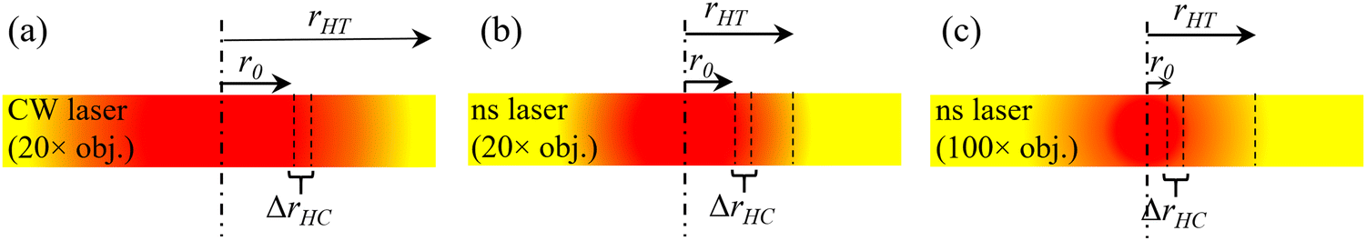 | ||
| Fig. 5 Cross-section view of heat diffusion length (rHT), laser spot radius (r0), and hot carrier diffusion length (ΔrHC) for three different cases: (a) 20× CW, (b) 20× ns, and (c) 100× ns laser heating. Here, the pulse width of nanosecond laser is 200 ns. Reproduced from ref. 34 with permission from Elsevier, copyright 2019. | ||
In another work, Yuan et al.7 developed an energy transport state-resolved Raman (ET-Raman) technique to distinguish hot carrier diffusion and interfacial energy transport in a few-layered MoS2 supported on c-Si. They differentiated the effects of R and D by constructing two steady heat conduction states with different laser spot sizes. This measurement was performed for MoS2 films with thicknesses from 6.6 nm to 17.4 nm. An increasing trend of D against thickness was observed, as shown in Fig. 6(b). Also shown in the figure is the measured interface thermal resistance variation against the film thickness. The slight decrease of R with film thickness is partly due to the increased film stiffness and the resulting better contact with the substrate.
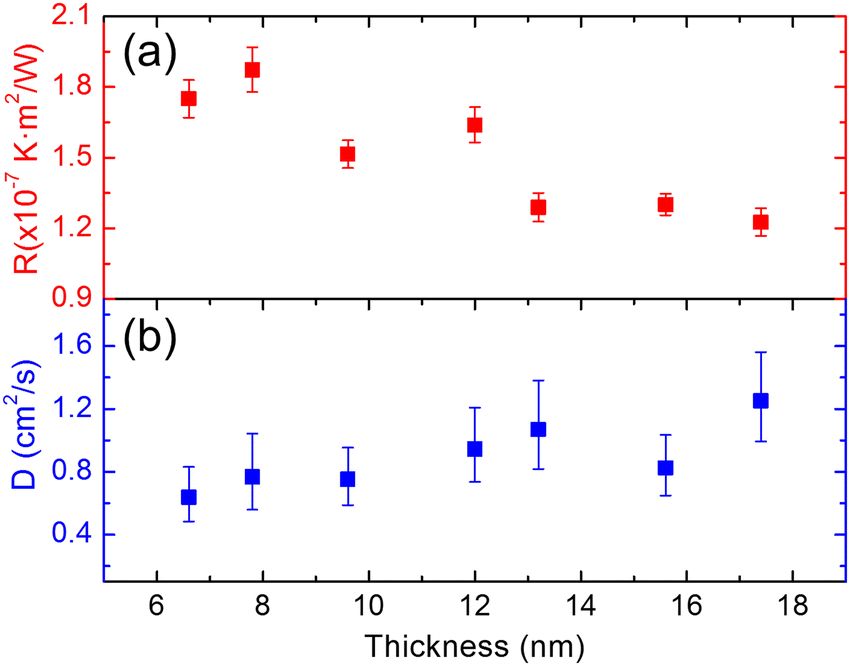 | ||
| Fig. 6 (a) Interface thermal resistance, and (b) hot carrier diffusion coefficient of seven MoS2 nm-thick films supported on c-Si. Reproduced from ref. 7 with permission from American Chemical Society, copyright 2017. | ||
Also, the effects of optical properties, especially refractive index, on D determination were studied. As an example, they reduced the real part of the refractive index of MoS2 by half in their ET-Raman-based numerical analysis and observed negligible effects on D (i.e., less than 1%) compared with that using the original value of the refractive index.
Yuan et al.35 also reported D of few-layered MoS2 on a glass substrate. They observed a nonmonotonic trend of D versus film's thickness, as shown in Fig. 7(b). Also shown in the figure are variation trends of κ and R against the layer number. This D variation trend was attributed to the reduced charge impurities for thin films, loose contact with the substrate, and possible wet substrate surface for thicker samples.
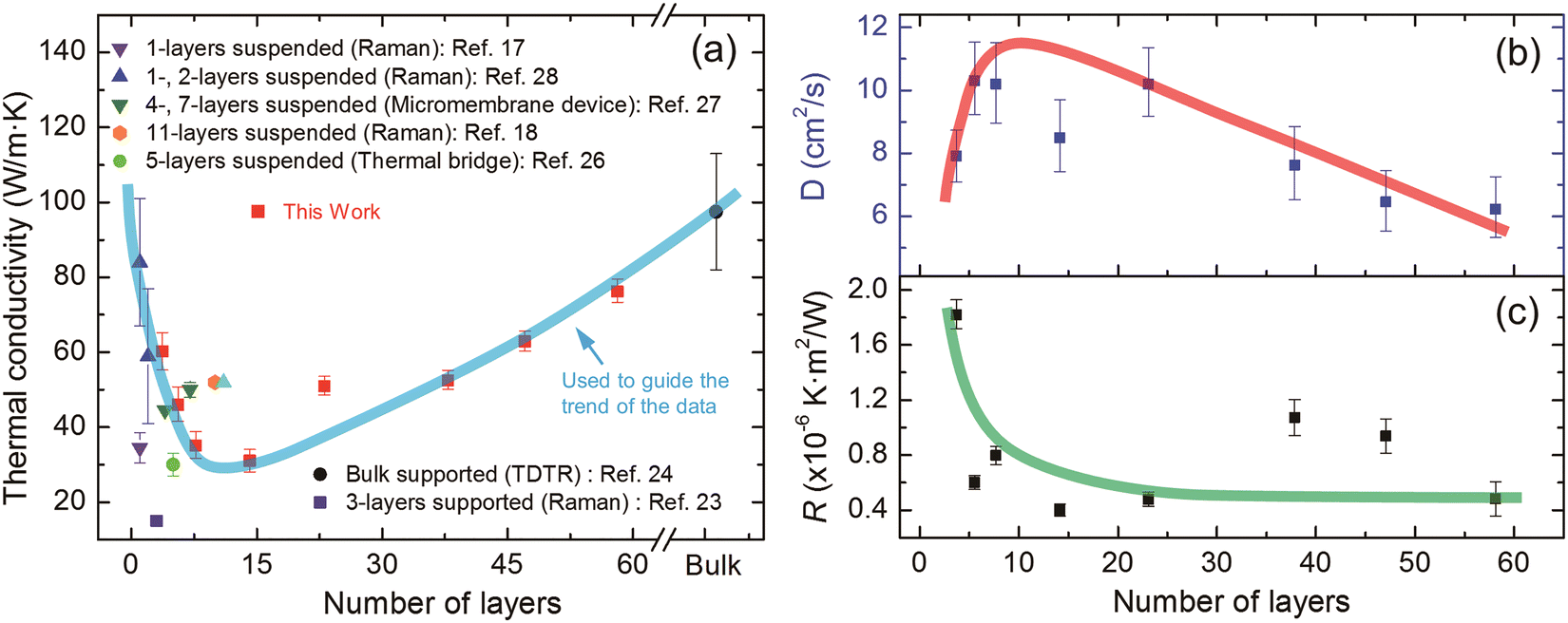 | ||
| Fig. 7 (a) In-plane thermal conductivity, (b) hot carrier diffusion coefficient, and (c) interface thermal resistance of multiple MoS2 films as a function of the film's number of layers. Reproduced from ref. 35 with permission from the PCCP Owner Societies, copyright 2018. | ||
4.2 Effects of physical parameters on D measurement
Zobeiri et al.34 reported the first results on D of suspended WS2 structures using a novel nanosecond ET-Raman (nET-Raman). They observed that the D value of all samples with different thicknesses is in a close range. This was attributed to similar lattice scattering for all of them, and there is no substrate effect. In that work, they studied the uncertainty caused by various parameters on the measured D. It was shown that a shorter laser pulse width of the nanosecond laser would lead to more precise measurement of D [Fig. 8(a)].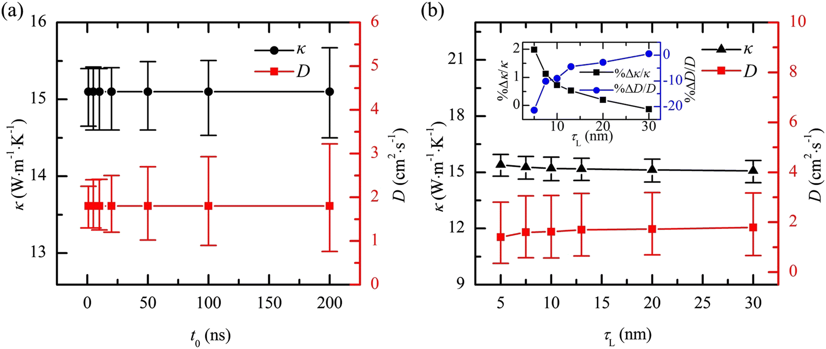 | ||
| Fig. 8 Effects of (a) laser pulse width and (b) laser absorption depth on the uncertainty of measured D (right vertical axis of both plots). Reproduced from ref. 34 with permission from Elsevier, copyright 2019. | ||
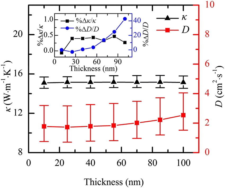
Another parameter that they studied was the laser absorption depth (τL). It was reported that τL has considerable effects on the measured D when it is much smaller than the thickness of the WS2 film. On the other hand, it has very negligible effects when τL is relatively large compared with the thickness of the suspended film [Fig. 8(b)]. They also reported the uncertainty caused by errors in the film thickness measurement. The result of this analysis is shown in Fig. 9 (right vertical axis).34 Note that these D values are extracted from the numerical calculations with these arbitrary thicknesses (x-axis) and experimental Raman data of a 13 nm sample. As an example, the uncertainty caused by this effect is less than 20% when the error of the thickness measurement is extremely large (i.e., 400%). They concluded that the error during the film thickness measurement has very little effect on their technique and D determination.
 | ||
| Fig. 9 Effect of the thickness measurement error on the uncertainty of determined D. Reproduced from ref. 34 with permission from Elsevier, copyright 2019. | ||
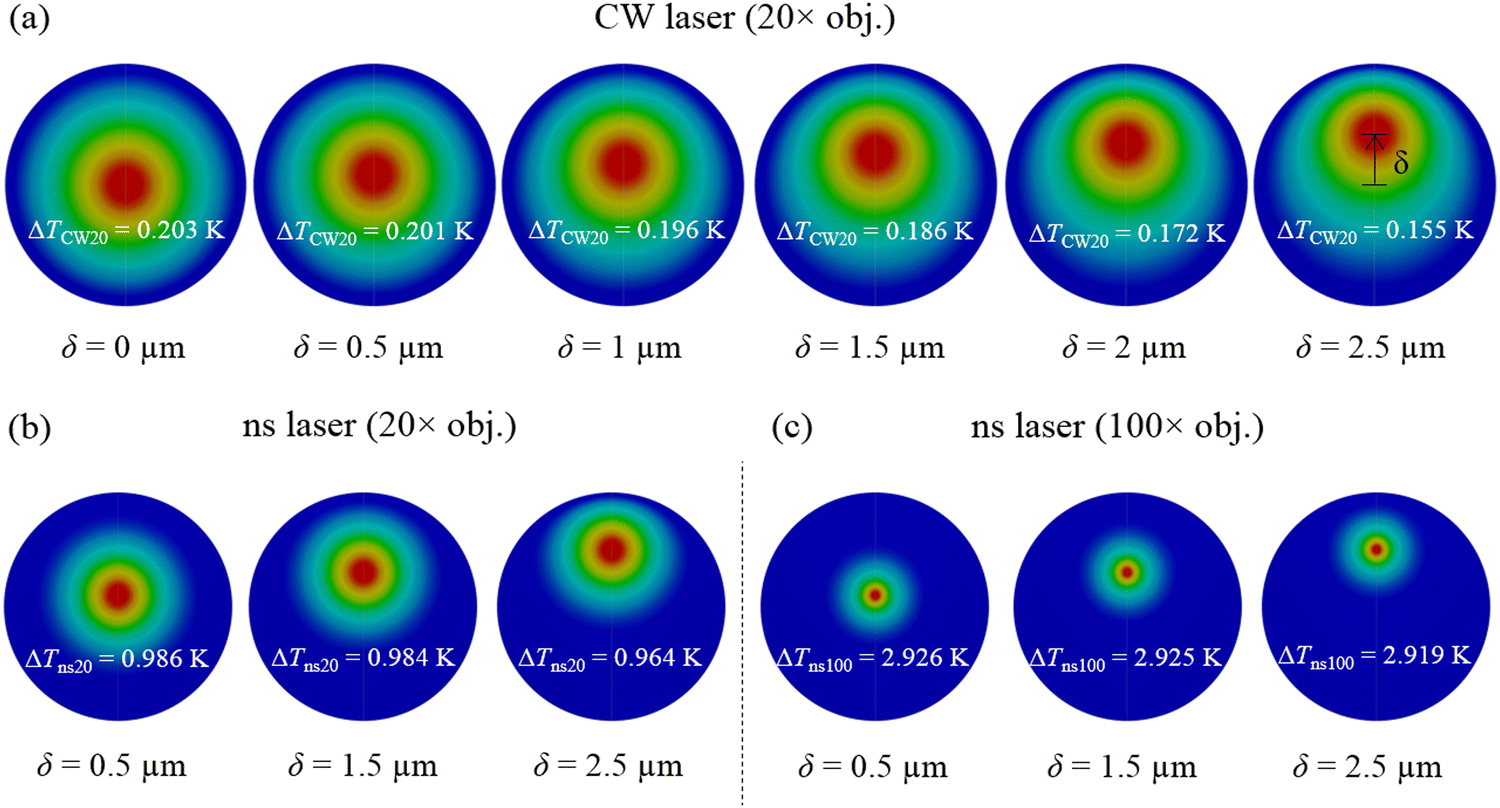
Additionally, they studied the effect of laser spot position (ns and CW laser spots) on their measurement accuracy. Fig. 10 shows the result of their numerical simulation. The radius of the suspended sample is 5 μm. All of the three different heating states were simulated (CW laser under 20× objective lens [Fig. 10(a)], ns laser under 20×, and 100× objective lens [Fig. 10(b and c)]). Since the laser spot size under the 100× lens is much smaller than the sample size, its location has little effect on the measurement. On the other hand, this laser spot deviation from the center of the sample has a significant effect on the measured D under 20× objective lens. For example, they reported that when the laser spot location under the CW laser is deviated by 1.5 μm, it leads to ∼90% uncertainty on the determined D. They concluded that it is necessary to ensure the laser spot location at the center of the suspended area for best measurement accuracy.
 | ||
| Fig. 10 Results of numerical analysis conducted by Zobeiri et al. to investigate the effect of laser spot position on the uncertainty of measured D of a suspended WS2 film. (a) CW laser heating (20×), (b) ns laser heating (20×), and (c) ns laser heating (100×). Reproduced from ref. 34 with permission from Elsevier, copyright 2019. | ||
4.3 An analysis on D measurement of supported thin films
Here, we present our in-depth numerical analysis to understand the effect of hot carrier diffusion in thermal characterization of the supported samples. To do so, two different setups are designed to perform our numerical simulation using a supported nm-thick MoS2 film: (1) over a Si substrate and (2) a SiO2 substrate. Details of this numerical analysis can be found in our previous works.12,25 Also, the optical properties of materials are consistent with the literature values.20,36,37 Based on these values, the laser absorption depth in a MoS2 film under a 532 nm laser is 32.33 nm. To consider the effects of D on the thermal transport inside the sample, two different calculations are performed for each geometry. In the first calculation, we assume that the D value is very small (in the order of 10−7 m2 s−1) and the Raman weighted average temperature rise under the CW laser was calculated: ΔTCW,0. In the other case, the temperature rise of the film was calculated when D is 7 × 10⁻⁴ m2 s−1: ΔTCW. This is a reasonable value of D for MoS2 and is based on literature values.7,11,35 Please see our previous works for more details about the calculation of Raman intensity weighted average temperature rise under steady-state laser heating.6,38 Wide ranges of laser spot size (r0) and film thickness are considered in our calculation to further study the D effect. Finally, a ΔTCW,0/ΔTCW ratio is calculated and represented as 2D contours for both cases, as shown in Fig. 11.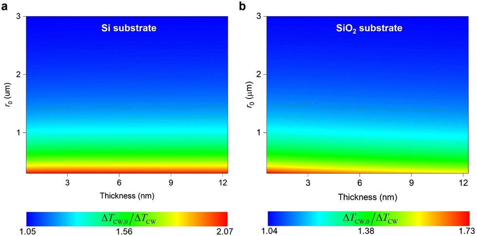 | ||
| Fig. 11 Calculated temperature rise ratio of a supported MoS2 film on (a) a Si, and (b) a SiO2 substrate. | ||
Comparing these two contours, we can reach several conclusions. First, the ΔTCW,0/ΔTCW ratio is larger when Si is the substrate (by comparing the contour values). This is due to the higher thermal conductivity of Si compared to SiO2, so the heat conduction in the in-plane direction is not significant, making the hot carrier effect more important. Second, the D effect is weaker for larger r0 values. This was discussed in Section 4.1 (see Fig. 5) by comparing the hot carrier diffusion length with r0. Third, both contours show a moderate effect of film thickness. For the SiO2 case, the ΔTCW,0/ΔTCW ratio is decreased for a specific r0 value when the film thickness is increased. This is because when the film is thicker, the in-plane heat conduction become more important, weakening the hot diffusion coefficient effect.
Note that most of the analyses described in this section to study the effects of laser pulse width, laser spot position, and film thickness are based on theoretical calculations. To do so, a numerical method based on the finite volume method was developed to calculate the temperature rise of the sample under each specific scenario. This method precisely solves the hot carrier diffusion equation and thermal diffusion equation.34 All of the related thermal and structural properties, such as thermal conductivity, hot carrier diffusion coefficient, electron–hole recombination time, laser pulse width, optical absorption coefficient, and equilibrium free carrier density were included in these studies.
5. Thermal nonequilibrium between optical and acoustic phonons
Regardless of different Raman-based methods used for energy transport characterization of 2D materials, the physical process is similar, as shown in Fig. 12, which consists of energy transfer among photons, electrons, and phonons. For phonons, there are three optical branches and three acoustic branches, both including longitudinal (LO and LA), transverse (TO and TA), and flexural branches (ZO and ZA). Moreover, the temperatures among these energy carriers are at nonequilibrium, especially the ZA phonons, which are the main heat carriers in heat conduction, showing the largest nonequilibrium from other phonon branches. Thus, neglect of nonequilibrium between the ZA phonons and LO/TO phonons probed by Raman spectroscopy can result in significant errors in energy transport characterization of nanomaterials by using Raman-based methods. Both theoretical simulation and experimental methods have been proposed to explore such thermal nonequilibrium.4,39–41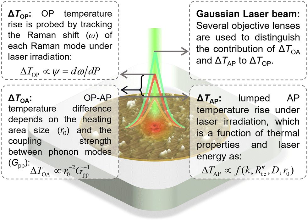 | ||
| Fig. 12 Physics of thermal nonequilibrium between OP and AP under laser irradiation. This figure shows the cascading energy transfer between two phonon modes within the heating area. Outside this area, OP and AP are in thermal equilibrium. Reprinted from ref. 41 with permission from Elsevier, copyright 2021. | ||
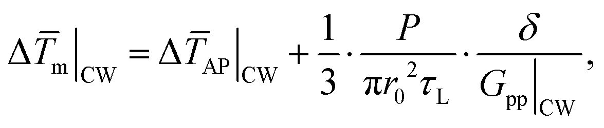
In 2020, for the first time, Wang et al.4 developed an ns ET-Raman technique to explore the thermal nonequilibrium among different phonon branches in a suspended 55 nm thick MoS2 and a suspended 71 nm thick MoSe2. To simplify the analysis, a lumped temperature rise Δ![[T with combining macron]](https://www.rsc.org/images/entities/i_char_0054_0304.gif) AP of the three acoustic phonon branches (LA, TA, and ZA) was used to represent the effect of the three branches. A finite volume-based three-dimensional (3D) model was employed to determine the lumped temperature rises under CW laser heating with different laser spot sizes. When the absorbed laser irradiation was 1 mW, this lumped temperature rise can be expressed as ΔAP|CW = 50 × (0.94 + 2.86e−1.65r0). Here, the 55 nm thick MoS2 under a CW laser and a 100× objective lens was used to do the calculation to demonstrate this strong nonequilibrium. The laser radius (r0) was around 0.405 μm, and the absorbed laser irradiation (P) was assumed to be 1 mW. Then, the temperature rise of APs was calculated to be 120.3 K. For the Raman-based characterization results, the Raman intensity weighted temperature rise under CW laser heating can be written as
AP of the three acoustic phonon branches (LA, TA, and ZA) was used to represent the effect of the three branches. A finite volume-based three-dimensional (3D) model was employed to determine the lumped temperature rises under CW laser heating with different laser spot sizes. When the absorbed laser irradiation was 1 mW, this lumped temperature rise can be expressed as ΔAP|CW = 50 × (0.94 + 2.86e−1.65r0). Here, the 55 nm thick MoS2 under a CW laser and a 100× objective lens was used to do the calculation to demonstrate this strong nonequilibrium. The laser radius (r0) was around 0.405 μm, and the absorbed laser irradiation (P) was assumed to be 1 mW. Then, the temperature rise of APs was calculated to be 120.3 K. For the Raman-based characterization results, the Raman intensity weighted temperature rise under CW laser heating can be written as
 | (4) |
m|CW, ψCW ∼ r0 relations of E2g1 and A1g modes are used to determine Gpp|CW values of these two modes, which are equal to 2.26 × 10¹⁴ and 1.18 × 10¹⁴ W m−3 K−1, respectively.4 Then, the temperature rise values obtained from E2g1 and A1g modes are calculated to be 173 and 170 K based on eqn (4), which are about 43.5% and 41.6% higher than the temperature rise of APs, respectively. For the 55 nm-thick MoS2 sample, the thermal conductivities obtained based on the A1g mode and E2g1 mode were 32.9 ± 2.3 and 24.4 ± 2.5 W m−1 K−1 under a 100× objective lens, respectively, when the thermal nonequilibrium was not considered. With the increased laser spot size, the difference between the two thermal conductivities was getting smaller. Under 20× objective lens, these two values converged to the same value, which was 46.9 ± 3.1 W m−1 K−1.4 Under such scenario, the thermal nonequilibrium is very weak and negligible. In summary, it is highly necessary to take the thermal nonequilibrium into consideration especially when a smaller laser spot is used in Raman-based methods.
In 2021, Zobeiri et al.41 further studied this thermal nonequilibrium in supported nanomaterials. Here, the 12.6 nm thick MoS2 on quartz under a CW laser and a 100× objective lens was used to perform the calculation to demonstrate this effect. The laser radius was around 0.42 μm, and the absorbed laser irradiation was assumed to be 1 mW. Similarly, the energy coupling strength between OP and AP also affects the heat conduction in supported nanomaterials. The local AP temperature rise ΔTAP depends on several parameters, including laser spot size (r0), thermal conductivity (κ), interfacial thermal resistance (R), and hot carrier diffusion (D). The OP temperature rise can be written as ΔTOP = ΔTAP + ΔTOA = ΔTAP + C/r02. C is the proportionality constant, which depends on the total absorbed laser energy and the energy coupling factor between OP and AP. Then, the contribution of ΔTOA to ΔTOP can be determined as  , where
  is defined as
 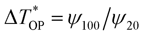 , ψ100 and ψ20 are Raman shift coefficients obtained under 100× and 20× objective lenses, respectively. Based on the above analysis, the temperature rises of E2g1 and A1g modes OPs are about 66.7% and 41.5% higher than the temperature rise of APs, respectively. Compared with suspended nanomaterials, the thermal nonequilibrium in supported nanomaterials is much more significant due to the fact that the supported sample could conduct the heat easier to the substrate through the interface. Therefore, a higher laser power, which leads to a larger ΔTOA, is needed in order to reach the same ΔTAP as the suspended one.
In summary, our analysis indicates that the thermal nonequilibrium, which is neglected in previous classical Raman-based energy transport characterization, is significant for both suspended and supported nanomaterials, especially under smaller heating areas (e.g. sub-μm). As a result, it is of great importance to take this phenomenon into account to realize much more accurate energy transport characterization for both suspended and supported nanomaterials.
6. Radiative electron–hole recombination in monolayer 2D materials
When it comes to monolayer 2D materials, any experimental thermal measurement holds its challenges and limitations. Opto-thermal Raman-based methods for determining interfacial thermal conductance (G) and κ of the monolayer materials have amply been demonstrated for their capacity for relatively simple, non-contact measurements. Although, as 2D TMD materials are reduced to single layers, the indirect to direct bandgap transition enhances photoluminescence and complicates Raman-based thermal measurements.As the Raman excitation laser energy is absorbed in the monolayer material, electron–hole pairs are generated. With a direct bandgap, the excited electrons in the conduction band now have a chance for radiative recombination with their respective holes across the bandgap. For the bulk and few-layered counterparts, the indirect bandgap assures only non-radiative recombination occurs in the form of phonon emission. In this case, opto-thermal Raman-based methods are perfectly adequate for thermal property measurements. However, in the case of monolayer TMD materials, neglecting the effect of radiative recombination will lead to the overestimation of G and κ since not all the absorbed laser energy is converted into heat.
While the rate of radiative recombination, also referred to as photoluminescence quantum yield (PL QY), in monolayer TMDs tends to be quite low (1–2%),42–45 experimental observations of ∼8% for both MoSe2 and WSe246 and up to ∼19% for WS247 have been reported. Additionally, as extensively discussed in our previous work, the material synthesis method, substrate, and defect density play critical roles in enhancing or impeding PL QY.6,42 We found that WSe2 monolayers fabricated on a fused silica substrate using the laser-assisted synthesis technique (LAST)48 yield PL QY values as high as 65%. Interestingly, other studies investigating as-exfoliated and as-grown CVD-synthesized WSe2 monolayers have reported radiative recombination rates of <3%.42,49,50 We attribute the large difference to the low level of impurities in the LAST monolayers (which limits nonradiative pathways). The potential low bonding strength between LAST monolayers and fused silica substrate also would explain the enhanced PL QY since it is known that decoupling 2D TMD monolayers from substrates increases photoluminescence.49
Given the extremely low levels of radiative recombination in the as-grown CVD-synthesized and mechanically exfoliated TMD monolayers, significant research investment has been made in finding ways to enhance the photoluminescence of these monolayers. Oftentimes, the enhancement techniques result in near-unity PL QY performance as is the case for WS2 monolayers chemically treated with an organic superacid, bis(trifluoromethane) sulfonimide (TFSI).47 Electrical suppression of nonradiative pathways has also shown to increase radiative recombination in MoS2 and WS2 up to 75% and 90%, respectively.46 Additionally, Liao et al.51 developed a photoactivation method to increase the PL QY of the monolayer MoS2 grown on silica micro/nanofibers up to 30%. Tailoring monolayer–substrate interactions has also resulted in enhanced PL QY. Kim et al.49 showed that a solvent evaporation-mediated decoupling (SEMD) technique releases surface tension between the grown monolayer and substrate and improves WSe2 radiative recombination by up ∼60%. Stress relaxation between MoS2 and a SiO2/Si substrate facilitated by ethanol treatment increased PL QY from <1% to 12%.45 A summary of radiative recombination rates for the untreated TMD monolayers and their corresponding improved PL QY from various enhancement techniques is shown in Table 2.
| Monolayer material | Preparation method | Substrate | Radiative recombination rate | Ref. |
|---|---|---|---|---|
| WSe2 | CVD/mechanical exfoliation | Fused silica | 2% | Ahn et al.42 |
| MoS2 | As-exfoliated | Quartz | 1% (98%) | Amani et al.47 |
| MoSe2 | 9% (4%) | |||
| WS2 | 19% (99%) | |||
| WSe2 | 3% (1%) | |||
| MoS2 | CVD | SiO2 (300 nm)/Si | <1% | Chen et al.43 |
| MoSe2 | <1% (16%) | |||
| WS2 | CVD | SiO2 (300 nm)/Si | <1% (9%) | Cui et al.44 |
| WSe2 | CVD | Fused silica | 1% (60%) | Kim et al.49 |
| MoS2 | CVD | Silica micro/nanofibers | <1% (30%) | Liao et al.51 |
| MoS2 | Mechanical exfoliation | PMMA/SiO2 | <1% (75%) | Lien et al.46 |
| WS2 | <2% (90%) | |||
| MoSe2 | 8% (5%) | |||
| WSe2 | 8% (2%) | |||
| WS2 | CVD | Sapphire | 6% (29%) | Liu et al.58 |
| MoS2 | Mechanical exfoliation | Si/SiOx | 8% | Salehzadeh et al.59 |
| WS2 | Physical vapor deposition (PVD) | SiO2/Si | <1% (12%) | Zheng et al.45 |
Clearly, a large window of radiative recombination rates is possible depending on material–substrate interactions, defect density, and enhancement strategy. Regardless of whether a PL QY enhancement technique has been applied, opto-thermal Raman methods for thermal characterizations of single-layer TMDs should consider radiative recombination effects for the most accurate evaluations of energy transport in these 2D nanostructures. Furthermore, once a TMD monolayer has been modified to increase radiative recombination, Raman-based techniques for G and κ determination will need to consider the non-negligible amount of laser energy absorbed and redirected towards photon emission rather than nonradiative pathways.
Currently, no opto-thermal Raman methods (besides ET-Raman) address the issue of radiative recombination in single-layer TMDs. In addition to the uncertainties introduced during Raman temperature calibration and laser absorption measurements, disregarding the photoluminescence of monolayer TMDs adds another layer of uncertainty to final thermal property measurements. Several works use laser irradiation for simultaneous Raman signal generation and sample heating. Easy et al.52 used a refined opto-thermal Raman technique to measure G and κ for suspended and supported WSe2 monolayers. Supported on a SiO2/Si substrate, a temperature-dependent Raman analysis revealed G to be 2.95 ± 0.46 MW m−2 K−1. Furthermore, substrate-supported monolayers showed a thermal conductivity of 37 ± 12 W m−1 K−1 while suspended samples showed κ of 49 ± 14 W m−1 K−1. Other works dependent on laser heating of monolayer samples and subsequent Raman analysis have shown monolayer MoS2 on SiO2/Si and SiO2/AlN substrates with G values of 17 ± 5 and 15 ± 4 MW m−2 K−1, respectively.53 Similar methods have determined thermal conductivities of 32 and 35 W m−1 K−1 for suspended monolayers of WS2 and MoS2, respectively.54,55
Raman thermometry techniques using electrical heating sources, rather than laser heating, have also been used to evaluate the thermal properties of monolayer TMDs. In this case, thermal generation becomes the primary driver of electron–hole pair generation instead of photogeneration. The same issue of radiative recombination in direct bandgap monolayer TMDs affects these techniques. Vaziri et al.50 have determined the interfacial thermal conductance between a heterostructure stack of single-layer graphene and MoS2 on a SiO2/Si substrate. The conductance across the monolayer TMD/substrate interface was measured to be 22 ± 4 MW m−2 K−1. Replacing the MoS2 monolayer with WSe2 resulted in a conductance value of 15 ± 4 MW m−2 K−1. Yalon et al.56 reported similar values for MoS2 also on a dioxide substrate as 14 ± 4 MW m−2 K−1. A summary of reported literature values for G and κ of monolayer TMDs is shown in Table 3.
| Monolayer material | Substrate | Preparation method | Interfacial thermal conductance [MW m−2 K−1] | Thermal conductivity [W m−1 K−1] | Ref. |
|---|---|---|---|---|---|
| WSe2 | SiO2/Si | Mechanical exfoliation | 2.95 ± 0.46 | 37 ± 12 | Easy et al.52 |
| Suspended (radius: 0.75 μm) | NA | 49 ± 14 | |||
| Graphene/WSe2 | SiO2/Si | CVD | 15 ± 4 | NA | Vaziri et al.50 |
| Graphene/MoS2 | 22 ± 4 | ||||
| MoS2 | SiO2/Si | CVD | 17 ± 5 | NA | Yalon et al.53 |
| SiO2/AlN | 15 ± 4 | ||||
| MoS2 | SiO2/Si | CVD | 14 ± 4 | NA | Yalon et al.56 |
| MoS2 | Sapphire | CVD | 17.4 ± 3.5 | NA | Yu et al.60 |
| SiO2/Si | CVD | 8.9 ± 1.6 | NA | ||
| Suspended (radius: 6.5 μm) | CVD (transferred) | NA | 97.4 ± 5.4 | ||
| WS2 | Sapphire | CVD | 30 ± 3 | NA | |
| Suspended (radius: 6.0 μm) | CVD (transferred) | NA | 118.2 ± 24.2 | ||
| WS2 | Suspended (radius: 1.5 μm) | CVD (transferred) | NA | 32 | Peimyoo et al.54 |
| MoS2 | Suspended (radius: 0.6 μm) | Mechanical exfoliation | NA | 34.5 ± 4 | Yan et al.55 |
In all the previously mentioned cases, radiative recombination is assumed to be negligible or disregarded. However, given the wide variety of factors influencing radiative recombination rates – including the numerous permutations of substrates, synthesis methods, and impurity concentrations for any given prepared monolayer TMD sample – more refined Raman-based techniques that consider radiative recombination are needed. This is especially true for monolayer TMD materials following photoluminescence enhancement techniques. As more methods are developed to improve the quantum yield of monolayer TMD materials for optoelectronic applications, Raman-based techniques that account for PL QY during experimental thermal characterizations will offer a distinct advantage over other methods.
One such method is the ET-Raman technique. The fundamental principle behind ET-Raman is to generate two or more distinct laser heating states in the spatial and/or temporal domain for the 2D material of interest. A normalized ratio formed by the different Raman shift power coefficients (∂ω/∂P) from the two distinct heating states can be equated to the corresponding normalized ratio of these numerically simulated temperature rises. The unique ratio analysis method nullifies the errors introduced from Raman temperature calibrations and laser absorption measurements. Most importantly, the radiative recombination effect will also be cancelled out through ratio analysis. This means the unique ratio formed from two distinct Raman shift power coefficients will provide precise temperature information free from the influence of absorbed laser energy lost through radiative recombination. Additionally, the ET-Raman method has been developed to accurately determine the PL QY of monolayer TMD materials through picosecond (ps) timescale heating. Since radiative lifetimes of room temperature monolayer TMDs happen at the nanosecond timescale,57 irradiating a monolayer sample with a ps-range laser pulse generates thermal transport that completely precedes all radiative e–h recombination. Combined with the accumulated heating effect for multiple pulses over a microsecond timescale when radiative recombination occurs, the ET-Raman method can easily distinguish and extract the rate of radiative recombination. The details of this method have been outlined extensively in our previous work.6 As investigations of the thermal properties of direct bandgap TMD monolayer materials continues, ET-Raman methods will continue to offer unique advantages for researchers interested in a comprehensive understanding of nanoscale energy transport.
7. Summary and outlook
As scatteredly discussed above, the ET-Raman technique was introduced to overcome the above problems. Fig. 13 shows the design of the ET-Raman technique to distinguish the energy transport in a 2D material, hot carrier transport, and energy transport across the interface.35 Use of different laser spot sizes can help suppress or magnify the effect of in-plane heat conduction, hot carrier diffusion, and interface energy transport. For instance, when the laser spot size is very small, the hot carrier diffusion becomes extremely important as it can quickly spread the absorbed laser energy out of the heating region. When the laser spot size is very large, the effects of both heat conduction and hot carrier diffusion in the 2D material will diminish and its temperature rise is largely determined by the interface thermal resistance.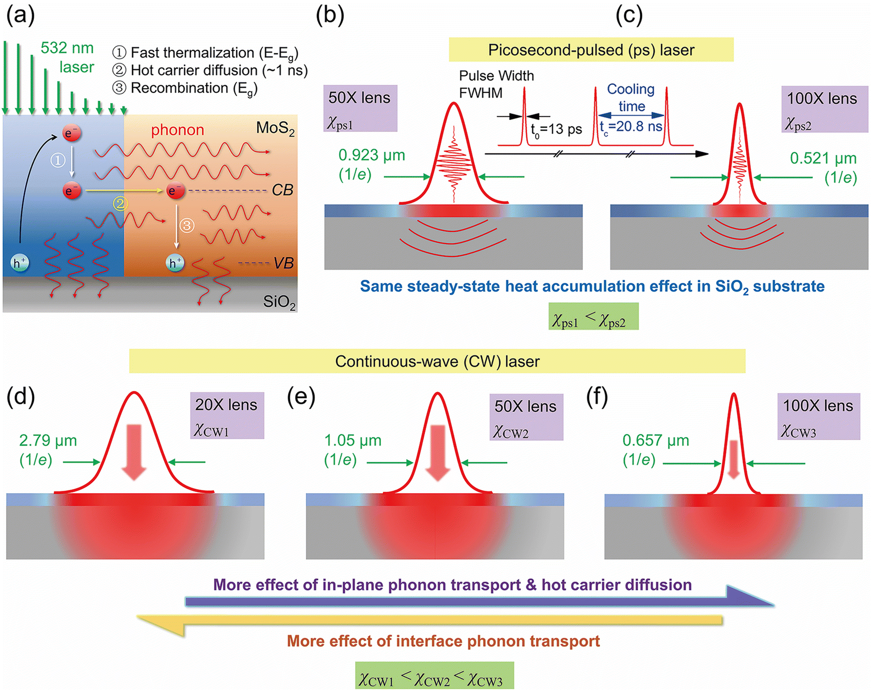 | ||
| Fig. 13 Design of the ET-Raman technique for simultaneous distinguishing and measurement of in-plane thermal conductivity, hot carrier diffusivity, and interface thermal resistance of 2D materials. (a) hot carrier generation, diffusion, and recombination, (b and c) transient state design with two different laser spot sizes, and (d–f) steady state design with three different laser spot sizes. Reproduced from ref. 35 with permission from the PCCP Owner Societies, copyright 2018. | ||
The introduction of transient laser heating and the simultaneous Raman measurement is intended to eliminate the requirement of absolute laser absorption and absolute temperature rise. The ratio (Θ) of the Raman shift power coefficient (steady state over the transient state: Θ = ψsteady/ψtransient) can completely eliminate the need for these two physical parameters. It should be noted that the introduction of this ratio somehow reduces the sensitivity of the measurement. For instance, for a supported 2D material, an increase in interface thermal resistance will increase the RSC of both steady and transient states. As a result, the ratio of the RSC of these two states will increase less against interface thermal resistance. This problem can be partially mediated by improving the Raman spectroscopy measurement accuracy.
The concept of transient laser heating and Raman probing was initially introduced in the time domain differential Raman (TD-Raman)61 and frequency-resolved Raman (FR-Raman).62 In addition to suspended 2D materials, the ET-Raman concept has also been applied to supported 2D materials in characterizing the thermal conductivity,12 hot carrier transport,34 and structure domain size.63 One should always be cautious about the interface thermal resistance measurement of supported 2D materials that have no constrain on their surface. As discussed in Section 3, localized heating and thermal expansion mismatch will always induce interface separation, which in turn significantly increases the local interface thermal resistance. Although the laser absorption and temperature rise evaluation problems are completely solved, this interface separation is always unavoidable. One possible way to solve this problem is to only induce a very low-temperature rise (about ∼1 K) of the 2D material, making the interface separation effect very small/negligible and the local interface van der Waals force can still hold the 2D material tightly to the substrate surface. Another way is to use a small 2D material, e.g. ∼μm in diameter. Therefore, when thermal expansion mismatch happens, the 2D material can easily expand or contract to release the local stress while still keeping the interface very tight.
For optical–acoustic phonon thermal nonequilibrium, the ET-Raman technique could also partially mediate its effect on the final measurement results. This is because the optical–acoustic phonon temperature difference will appear in both steady state and transient laser heating and Raman probing. Therefore, Θ will have much less effect from the optical–acoustic thermal nonequilibrium. However, distinguishing and subtracting the effect of optical–acoustic phonon thermal nonequilibrium remains a big challenge in the thermal transport characterization of 2D materials. Future techniques are expected to build rigorous physical models for probing and subtracting this effect. This is urgently needed to advance the scientific understanding of thermal transport in 2D materials and to tailor their structure toward specific thermal performance requirements.
As the ET-Raman technique does not need the laser absolution value, this naturally eliminates the problem of electron–hole radiative recombination in the monolayer 2D materials. Also, the transient state design in the picosecond scale provides a novel way to precisely determine the radiative recombination efficiency.6 Future studies of monolayer 2D materials could use other ways to identify the radiative electron–hole recombination and subtract its effect or use techniques such as the ET-Raman to work out this problem. In ET-Raman, pulsed lasers are used to realize transient heating and Raman probing. Sometimes this suffers from low Raman signal level due to the low repetition rate of the pulsed laser. Also, precaution should be taken when choosing the laser energy as the laser energy is constrained within one pulse and the very high laser intensity could cause structural damage. A good idea is to choose the repetition rate as high as possible while keeping the pulse interval long enough to allow the sample to cool down before the next pulse comes in. However, for picosecond lasers, the repetition rate usually is very high (tens of MHz). So the accumulation of pulse heating will happen. The physical model must rigorously consider this effect. The FET-Raman can solve this problem while still featuring the great physical advantages of ET-Raman.25,64 The FET-Raman can generate frequencies whose time scale is at the same level as the pulse width of a pulsed laser. This will greatly improve the signal level in Raman measurement and significantly suppress the noise effect. Also because the Raman integration time is significantly reduced, the sample stage shift can be reduced to a minimal level. All of these will lead to significantly improved measurement accuracy.
Conflicts of interest
There are no conflicts to declare.Acknowledgements
The support of this work by the National Science Foundation (No. CBET1930866 and CMMI2032464 for X. W.) is gratefully acknowledged. Partial support of this work by the National Natural Science Foundation of China (No. 52005367 for R. W. and No. 52106220 for S. X.) is gratefully acknowledged.References
- K. S. Novoselov, A. K. Geim, S. V. Morozov, D. Jiang, Y. Zhang, S. V. Dubonos, I. V. Grigorieva and A. A. Firsov, Science, 2004, 306, 666–669 CrossRef CAS PubMed.
- Y. Yue, J. Zhang and X. Wang, Small, 2011, 7, 3324–3333 CrossRef CAS PubMed.
- J. Gao, H. Zobeiri, H. Lin, D. Xie, Y. Yue and X. Wang, Carbon, 2021, 178, 92–102 CrossRef CAS.
- R. Wang, H. Zobeiri, Y. Xie, X. Wang, X. Zhang and Y. Yue, Adv. Sci., 2020, 7, 2000097 CrossRef CAS PubMed.
- R. Wang, S. Xu, Y. Yue and X. Wang, Int. J. Extreme Manuf., 2020, 2, 032004 CrossRef CAS.
- N. Hunter, N. Azam, H. Zobeiri, R. Wang, M. Mahjouri-Samani and X. Wang, ACS Appl. Mater. Interfaces, 2020, 12, 51069–51081 CrossRef CAS PubMed.
- P. Yuan, R. Wang, H. Tan, T. Wang and X. Wang, ACS Photon., 2017, 4, 3115–3129 CrossRef CAS.
- T. Wang, J. Liu, B. Xu, R. Wang, P. Yuan, M. Han, S. Xu, Y. Xie, Y. Wu and X. Wang, ChemPhysChem, 2017, 18, 2828–2834 CrossRef CAS PubMed.
- S. Xu, A. Fan, H. Wang, X. Zhang and X. Wang, Int. J. Heat Mass Transfer, 2020, 154, 119751 CrossRef CAS.
- Y. Yue, J. Zhang, Y. Xie, W. Chen and X. Wang, Int. J. Heat Mass Transfer, 2017, 110, 827–844 CrossRef CAS.
- P. Yuan, J. Liu, R. Wang and X. Wang, Nanoscale, 2017, 9, 6808–6820 RSC.
- R. Wang, T. Wang, H. Zobeiri, P. Yuan, C. Deng, Y. Yue, S. Xu and X. Wang, Nanoscale, 2018, 10, 23087–23102 RSC.
- C. Yim, M. O'Brien, N. McEvoy, S. Winters, I. Mirza, J. G. Lunney and G. S. Duesberg, Appl. Phys. Lett., 2014, 104, 103114 CrossRef.
- H. Zhang, Y. Ma, Y. Wan, X. Rong, Z. Xie, W. Wang and L. Dai, Sci. Rep., 2015, 5, 8440 CrossRef CAS PubMed.
- Z. Lu, A. Vallabhaneni, B. Cao and X. Ruan, Phys. Rev. B, 2018, 98, 134309 CrossRef CAS.
- X. Tang, S. Xu and X. Wang, Nanoscale, 2014, 6, 8822–8830 RSC.
- X. Tang, S. Xu, J. Zhang and X. Wang, ACS Appl. Mater. Interfaces, 2014, 6, 2809–2818 CrossRef CAS PubMed.
- N. V. Velson, H. Zobeiri and X. Wang, Opt. Express, 2020, 28, 35272–35283 CrossRef PubMed.
- M. S. Diware, K. Park, J. Mun, H. G. Park, W. Chegal, Y. J. Cho, H. M. Cho, J. Park, H. Kim, S.-W. Kang and Y. D. Kim, Curr. Appl. Phys., 2017, 17, 1329–1334 CrossRef.
- C. Schinke, P. Christian Peest, J. Schmidt, R. Brendel, K. Bothe, M. R. Vogt, I. Kröger, S. Winter, A. Schirmacher, S. Lim, H. T. Nguyen and D. MacDonald, AIP Adv., 2015, 5, 067168 CrossRef.
- I. H. Malitson, J. Opt. Soc. Am., 1965, 55, 1205–1209 CrossRef CAS.
- R. Addou, L. Colombo and R. M. Wallace, ACS Appl. Mater. Interfaces, 2015, 7, 11921–11929 CrossRef CAS PubMed.
- P. Yuan, H. Tan, R. Wang, T. Wang and X. Wang, RSC Adv., 2018, 8, 12767–12778 RSC.
- D. Yoon, H. Moon, Y.-W. Son, J. S. Choi, B. H. Park, Y. H. Cha, Y. D. Kim and H. Cheong, Phys. Rev. B, 2009, 80, 125422 CrossRef.
- H. Zobeiri, R. Wang, T. Wang, H. Lin, C. Deng and X. Wang, Int. J. Heat Mass Transfer, 2019, 133, 1074–1085 CrossRef CAS.
- D. J. Late, S. N. Shirodkar, U. V. Waghmare, V. P. Dravid and C. N. R. Rao, ChemPhysChem, 2014, 15, 1592–1598 CrossRef CAS PubMed.
- X. Zhang, X.-F. Qiao, W. Shi, J.-B. Wu, D.-S. Jiang and P.-H. Tan, Chem. Soc. Rev., 2015, 44, 2757–2785 RSC.
- L. Su, Y. Yu, L. Cao and Y. Zhang, Nano Res., 2015, 8, 2686–2697 CrossRef CAS.
- Z. Lin, W. Liu, S. Tian, K. Zhu, Y. Huang and Y. Yang, Sci. Rep., 2021, 11, 7037 CrossRef CAS PubMed.
- L. Su, Y. Zhang, Y. Yu and L. Cao, Nanoscale, 2014, 6, 4920–4927 RSC.
- K. K. Madapu and S. Dhara, AIP Adv., 2020, 10, 085003 CrossRef CAS.
- Z. Liu, M. Amani, S. Najmaei, Q. Xu, X. Zou, W. Zhou, T. Yu, C. Qiu, A. G. Birdwell, F. J. Crowne, R. Vajtai, B. I. Yakobson, Z. Xia, M. Dubey, P. M. Ajayan and J. Lou, Nat. Commun., 2014, 5, 5246 CrossRef PubMed.
- H. J. Conley, B. Wang, J. I. Ziegler, R. F. Haglund, S. T. Pantelides and K. I. Bolotin, Nano Lett., 2013, 13, 3626–3630 CrossRef CAS PubMed.
- H. Zobeiri, R. Wang, Q. Zhang, G. Zhu and X. Wang, Acta Mater., 2019, 175, 222–237 CrossRef CAS.
- P. Yuan, R. Wang, T. Wang, X. Wang and Y. Xie, Phys. Chem. Chem. Phys., 2018, 20, 25752–25761 RSC.
- B. Song, H. Gu, M. Fang, X. Chen, H. Jiang, R. Wang, T. Zhai, Y. T. Ho and S. Liu, Adv. Opt. Mater., 2019, 7, 1801250 CrossRef.
- C. Z. Tan, J. Non-Cryst. Solids, 1998, 223, 158–163 CrossRef CAS.
- N. Hunter, H. Zobeiri, T. Wang and X. Wang, Int. J. Heat Mass Transfer, 2021, 179, 121644 CrossRef CAS.
- Z. Lu and X. Ruan, ES Energy Environ., 2019, 4, 5–14 Search PubMed.
- B. P. Falcão, J. P. Leitão, M. R. Correia, M. R. Soares, H. Wiggers, A. Cantarero and R. N. Pereira, Phys. Rev. B, 2017, 95, 115439 CrossRef.
- H. Zobeiri, N. Hunter, N. Van Velson, C. Deng, Q. Zhang and X. Wang, Nano Energy, 2021, 89, 106364 CrossRef CAS.
- G. H. Ahn, M. Amani, H. Rasool, D.-H. Lien, J. P. Mastandrea, J. W. Ager Iii, M. Dubey, D. C. Chrzan, A. M. Minor and A. Javey, Nat. Commun., 2017, 8, 608 CrossRef PubMed.
- K. Chen, S. Deng, E. Chen, S. Wen, T. Ouyang, X. Wang, R. Zhan, J. Cai, X. Wan and H. Chen, ACS Appl. Mater. Interfaces, 2021, 13, 44814–44823 CrossRef CAS PubMed.
- Q. Cui, Z. Luo, Q. Cui, W. Zhu, H. Shou, C. Wu, Z. Liu, Y. Lin, P. Zhang, S. Wei, H. Yang, S. Chen, A. Pan and L. Song, Adv. Funct. Mater., 2021, 31, 2105339 CrossRef CAS.
- B. Zheng, W. Zheng, Y. Jiang, S. Chen, D. Li, C. Ma, X. Wang, W. Huang, X. Zhang, H. Liu, F. Jiang, L. Li, X. Zhuang, X. Wang and A. Pan, J. Am. Chem. Soc., 2019, 141, 11754–11758 CrossRef CAS PubMed.
- D.-H. Lien, Z. Uddin Shiekh, M. Yeh, M. Amani, H. Kim, W. Ager Joel, E. Yablonovitch and A. Javey, Science, 2019, 364, 468–471 CrossRef CAS PubMed.
- M. Amani, P. Taheri, R. Addou, G. H. Ahn, D. Kiriya, D.-H. Lien, J. W. Ager, R. M. Wallace and A. Javey, Nano Lett., 2016, 16, 2786–2791 CrossRef CAS PubMed.
- N. Azam, Z. Ahmadi, B. Yakupoglu, S. Elafandi, M. Tian, A. Boulesbaa and M. Mahjouri-Samani, 2D Mater., 2019, 7, 015014 CrossRef.
- H. Kim, H. Ahn Geun, J. Cho, M. Amani, P. Mastandrea James, K. Groschner Catherine, D.-H. Lien, Y. Zhao, W. Ager Joel, C. Scott Mary, C. Chrzan Daryl and A. Javey, Sci. Adv., 2019, 5, eaau4728 CrossRef PubMed.
- S. Vaziri, E. Yalon, M. Muñoz Rojo, V. Suryavanshi Saurabh, H. Zhang, J. McClellan Connor, S. Bailey Connor, K. H. Smithe Kirby, J. Gabourie Alexander, V. Chen, S. Deshmukh, L. Bendersky, V. Davydov Albert and E. Pop, Sci. Adv., 2019, 5, eaax1325 CrossRef CAS PubMed.
- F. Liao, J. Yu, Z. Gu, Z. Yang, T. Hasan, S. Linghu, J. Peng, W. Fang, S. Zhuang, M. Gu and F. Gu, Sci. Adv., 2019, 5, eaax7398 CrossRef CAS PubMed.
- E. Easy, Y. Gao, Y. Wang, D. Yan, S. M. Goushehgir, E.-H. Yang, B. Xu and X. Zhang, ACS Appl. Mater. Interfaces, 2021, 13, 13063–13071 CrossRef CAS PubMed.
- E. Yalon, Ö. B. Aslan, K. K. H. Smithe, C. J. McClellan, S. V. Suryavanshi, F. Xiong, A. Sood, C. M. Neumann, X. Xu, K. E. Goodson, T. F. Heinz and E. Pop, ACS Appl. Mater. Interfaces, 2017, 9, 43013–43020 CrossRef CAS PubMed.
- N. Peimyoo, J. Shang, W. Yang, Y. Wang, C. Cong and T. Yu, Nano Res., 2015, 8, 1210–1221 CrossRef CAS.
- R. Yan, J. R. Simpson, S. Bertolazzi, J. Brivio, M. Watson, X. Wu, A. Kis, T. Luo, A. R. Hight Walker and H. G. Xing, ACS Nano, 2014, 8, 986–993 CrossRef CAS PubMed.
- E. Yalon, C. J. McClellan, K. K. H. Smithe, M. Muñoz Rojo, R. L. Xu, S. V. Suryavanshi, A. J. Gabourie, C. M. Neumann, F. Xiong, A. B. Farimani and E. Pop, Nano Lett., 2017, 17, 3429–3433 CrossRef CAS PubMed.
- M. Palummo, M. Bernardi and J. C. Grossman, Nano Lett., 2015, 15, 2794–2800 CrossRef CAS PubMed.
- Y. Liu, H. Li, X. Zheng, X. Cheng and T. Jiang, Opt. Mater. Express, 2017, 7, 1327–1334 CrossRef CAS.
- O. Salehzadeh, N. H. Tran, X. Liu, I. Shih and Z. Mi, Nano Lett., 2014, 14, 4125–4130 CrossRef CAS PubMed.
- Y. Yu, T. Minhaj, L. Huang, Y. Yu and L. Cao, Phys. Rev. Appl., 2020, 13, 034059 CrossRef CAS.
- S. Xu, T. Wang, D. Hurley, Y. Yue and X. Wang, Opt. Express, 2015, 23, 10040–10056 CrossRef CAS PubMed.
- T. Wang, S. Xu, D. H. Hurley, Y. Yue and X. Wang, Opt. Lett., 2016, 41, 80–83 CrossRef CAS PubMed.
- H. Lin, R. Wang, H. Zobeiri, T. Wang, S. Xu and X. Wang, Nanoscale, 2021, 13, 7723–7734 RSC.
- R. Wang, H. Zobeiri, H. Lin, W. Qu, X. Bai, C. Deng and X. Wang, Carbon, 2019, 147, 58–69 CrossRef CAS.
Footnote |
| † Equal contribution authors. |
| This journal is © the Owner Societies 2022 |