
Ultrafast dynamics of spin relaxation in monolayer WSe2 and the WSe2/graphene heterojunction
Xin
Chen
,
Shu-Wen
Zheng
,
Xue-Peng
Wang
 and
Hai-Yu
Wang
*
and
Hai-Yu
Wang
*
State Key Laboratory of Integrated Optoelectronics, College of Electronic Science and Engineering, Jilin University, 2699 Qianjin Street, Changchun 130012, China. E-mail: haiyu_wang@jlu.edu.cn
First published on 27th June 2022
Abstract
Excitonic devices based on two-dimensional (2D) transition metal dichalcogenides (TMDCs) can combine spintronics with valleytronics due to its special energy band structure. In this work, we studied the generation and relaxation processes of spin/valley polarized excitons dynamics in monolayer WSe2 and its van der Waals (vdW) heterojunction with graphene using a circularly polarized femtosecond pump–probe system. The spin/valley depolarization dynamics of the A exciton in monolayer WSe2 is found to exhibit a biexponential decay. The fast relaxation process is due to the ultrafast intervalley electron–hole spin–flip exchange coupling and electron–phonon scattering. And the slow relaxation process originates from the recombination and relaxation of the trion states. Graphene has an electron extraction effect on WSe2, which prevents the formation of trions. Therefore, the spin/valley depolarization process of the A exciton in the heterojunction exhibits only a fast relaxation process. In both monolayer WSe2 and its heterojunction with graphene, B/A′ excitons exhibit a negative spin/valley polarization which is mainly due to two-photon absorption and excited Bose scattering. Our work systematically studied the spin/valley depolarization dynamics of excitons and revealed possible mechanisms of their differences in isolated 2D WSe2 and vdW heterojunctions.
Introduction
Two-dimensional (2D) transition metal dichalcogenides (TMDCs) have attracted extensive attention not only because of their applications in electron transport devices,1 but also because they are a good platform for studying light–matter interactions as well as unique photophysical phenomena.2–6 For example, due to their direct bandgap feature,7 2D TMDCs are particularly suitable for valleytronic studies including optical probing and controlling of valley degrees of freedom, investigation on optical selection rules8,9 and the valley Hall effect (VHE).10,11 On the other hand, as the first two-dimensional material to be isolated, graphene has also made a major breakthrough in valleytronics.12 For example, graphene grown via CVD could exhibit a high mobility13 of 3 × 106 cm2 s−1 V−1 and a spin lifetime of 12 ns.14In recent years, 2D TMDC/graphene van der Waals heterojunctions have attracted significant attention due to the ability of combining the unique properties of both components.15–20 Even though TMDCs and graphene are connected by the relatively weak van der Waals (vdW) forces in the vdW heterojunctions, they could still affect each other or generate new interface phenomena due to the proximity effects.19 The semi-metallic nature of graphene can reduce or even eliminate the Schottky barrier between 2D TMDC/metal contacts, which could modulate the electronic properties of 2D TMDCs.20 In addition, 2D TMDCs exhibit strong spin–orbit coupling (SOC) and spin valley coupling. Recent studies have shown that this can be used to control the spin degrees of freedom of graphene through the vdW heterojunction.15–20 For example, it has been reported that MoS2 could induce spin polarization of graphene by optical pump injection.21–24 So, MoS2/graphene heterojunction can act as a logical spin valve in which the on/off switching is achieved by adjusting the Fermi level.21,22 As a TMDC, monolayer WSe2 has also been reported to generate spin polarization.25,26 For example, by time-resolved spectroscopy, Ye et al. investigated the ultrafast dynamics of spin generation and relaxation in monolayer WSe2.25 However, works on the effect of graphene on the valley polarization dynamics of monolayer WSe2 are still rare.
In this work, by circularly polarized ultrafast spectroscopy, we systematically study the polarization and depolarization dynamics of excitons in monolayer WSe2 and its vdW heterojunction with graphene. The polarization behavior of A, B, and A′ excitons in these structures are clearly investigated. We also reveal the possible valley depolarization mechanism to describe the key physical process of coherent/collisional spin relaxation dynamics and demonstrate the electron extraction effect of graphene. Our findings give possible way to understand the spin/valley polarization behavior in the excitonic devices based on 2D TMDCs and their vdW heterojunction.
Results and discussion
Fig. 1(a) shows the atomic structure of the WSe2/graphene vdW heterojunction. By first-principles calculations, we obtained and compared the electronic structures of isolated monolayer WSe2 and the WSe2/graphene vdW heterojunction. Fig. 1(b and c) shows the element specific density of states (DOS) of monolayer WSe2 and the WSe2/graphene vdW heterojunction, respectively. It seems that graphene has little impact on the DOS of WSe2. In contrast, a significant energy gap can be identified in the DOS of graphene. So, WSe2 could affect the electronic structure and open band gap of graphene. According to the DOS of the vdW heterojunction, the VBM and CBM are mainly contributed by C atoms. That means that the CBM of graphene is lower than that of monolayer WSe2. Therefore, it can be expected that the excited electrons will transfer from WSe2 to graphene. In other words, graphene could extract electrons from WSe2.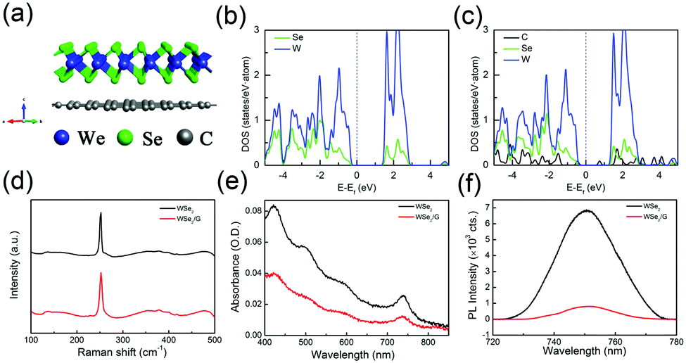 | ||
| Fig. 1 (a) Atomic structure of the WSe2/graphene vdW heterojunction. Atomic colors: blue for W, green for Se, and gray for C. (b) Density of states (DOS) of W and Se in monolayer WSe2. (c) DOS of W, Se and C in the WSe2/graphene vdW heterojunction. (d) Raman spectra, (e) steady-state absorption spectra, and (f) PL spectra of monolayer WSe2 and the WSe2/graphene (WSe2/G) vdW heterojunction, respectively. | ||
In experiment, we obtained the Raman spectra of monolayer WSe2 and the WSe2/graphene vdW heterojunction under a 532 nm excitation. As displayed in Fig. 1(d), the two samples show the same characteristic peaks. The E2g1 peak at 252.5 cm−1 comes from the in-plane vibrational modes and degenerates to the A1g peak that originates from the out-of-plane vibrational modes. The 2LA(M) peak (the second-order Raman mode caused by LA phonons at the M point in the Brillouin zone) is located at 263.4 cm−1, just near the A1g peak. Fig. 1(e) shows the steady-state absorption spectra of the two samples. The absorption spectra of both monolayer WSe2 and the WSe2/graphene vdW heterojunction exhibit peaks at 420 nm, 499 nm, 590 nm, and 740 nm, corresponding to the transitions of C, A′, B, and A excitons, respectively. Fig. 1(f) displays the photoluminescence (PL) spectra of monolayer WSe2 and the WSe2/graphene vdW heterojunction. Both samples have a PL peak at ∼750 nm. But the PL intensity of monolayer WSe2 is much higher (about 7 times) than that of the vdW heterojunction. According to our first-principles calculation results, graphene could extract photogenerated carriers from WSe2. That's why we observe a reduction of PL intensity in the vdW heterojunction.
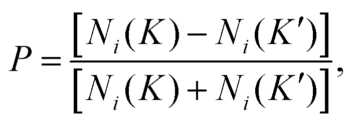
It has been reported that monolayer WSe2 has a direct bandgap and two non-equivalent valleys (K/K′) at the corners of its hexagonal Brillouin zone. There will be energy splitting in the valence and conduction bands due to a combined effect of the following reasons: the breaking of inversion symmetry, strong spin–orbit coupling (SOC), and the spin and valley coupling of carriers. It has been reported that the valence band of monolayer WSe2 has an energy splitting of about 400 meV while the splitting of conduction band is only about 37 meV.25 The spin/valley polarization dynamics behaviour of excitons can be reflected by the transient absorption spectra under a circularly polarized excitation. The spin/valley polarization is defined as
 | (1) |
 | (2) |
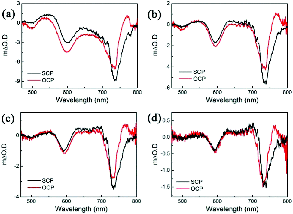
First, we performed a near-resonant excitation of the A-exciton. The exciton generation time is about 0.3 ps. Fig. 2 shows the SCP and OCP TA spectra under different pump fluences (delay time ∼0.3 ps). The transient absorption peaks of monolayer WSe2 appear at 499 nm (A′ exciton), 590 nm (B exciton) and 738 nm (A exciton), respectively. Obviously, the A exciton has a larger ΔODSCP compared with ΔODOCP, which implies a positive spin/valley polarization. In contrast, the spin/valley polarizations of B and A′ are negative. As mentioned above, the value of spin/valley polarization can be calculated based on ΔODSCP and ΔODOCP of each exciton. As shown in Table 1, the spin/valley polarization of A exciton monotonically decreases from 0.33 to 0.10 when the pump fluence decreases from 5.74 μJ cm−2 to 0.52 μJ cm−2 while the negative spin/valley polarizations of B and A′ excitons keep decreasing as pump fluence decreases. In particular, the spin/valley polarization of the two excitons becomes 0 upon 0.52 μJ cm−2, which means no valley polarization.
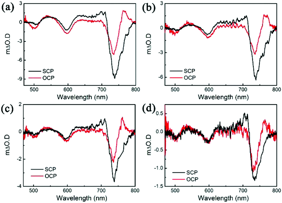 | ||
| Fig. 2 The SCP and OCP TA spectra of monolayer WSe2 (delay time ∼0.3 ps) with a pump fluence of (a) 5.74 μJ cm−2, (b) 2.61 μJ cm−2, (c) 1.30 μJ cm−2, and (d) 0.52 μJ cm−2. | ||
| Pump fluence (μJ cm−2) | A exciton | B exciton | A′ exciton |
|---|---|---|---|
| 5.74 | 0.33 | −0.23 | −0.45 |
| 2.61 | 0.27 | −0.19 | −0.42 |
| 1.30 | 0.24 | −0.17 | −0.32 |
| 0.52 | 0.10 | 0 | 0 |
Then, we fix the pump fluence to be 5.74 μJ cm−2 and investigate the spin/valley polarization dynamics of each exciton in monolayer WSe2. Fig. 3(a–c) show the transient absorption spectra (ΔOD) as a function of delay time of A, B, and A′ excitons in monolayer WSe2. According to Fig. 3(a), the A exciton exhibits OCP signal immediately after excitation. This implies the scattering of the excited A exciton into the non-pumped K′ valley due to the ultrafast inter-valley electron–hole spin–flip exchange coupling (A(K) → A(K′)), as demonstrated in previous works.25 We could also calculate the time-dependent spin/valley polarization P(t) based on eqn (2). As shown in Fig. 3(d), the A exciton has a positive spin/valley polarization in the whole 100 ps after excitation.
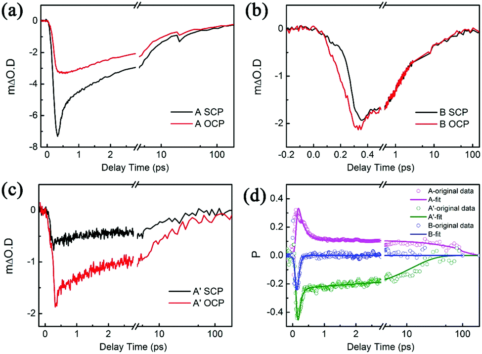 | ||
| Fig. 3 Transient absorption spectra (ΔOD) of (a) A, (b) B, and (c) A′ exciton in monolayer WSe2. (d) Time-dependent spin/valley polarization P of A (magenta), B (blue) and A′ (green) excitons at different delay times in monolayer WSe2. | ||
Since we performed the near-resonant excitation of the A exciton, in principle, the B exciton state in the K valley will not form due to the relative larger energy compared with the A exciton. However, we could still observe the ultrafast change of SCP and OCP of the B exciton in Fig. 3(b). That means that the polarized B exciton is generated in both K and K′ valleys. Furthermore, the B exciton has a negative spin/valley polarization especially in the initial 1 ps as shown in Fig. 3(d). This may be due to two possible mechanisms: one is two-photon absorption and stimulated Bose scattering, in which the A exciton state acts as an intermediate state.27 In this process, electrons firstly adsorb two photons and excited to a high-energy continuum state |f >, which is higher than the B and A exciton states, as shown in Fig. 4(a). The absorption of this high-energy continuum state is not constrained by the strict polarization selection rule. Therefore, the same population of σ+ excitons and σ− excitons can be generated in the high-energy continuum state. Then, the σ+ and σ− electron–hole pairs in the |f> state will relax to the lower B exciton state at the same rate, as shown in Fig. 4(b). Meanwhile, the B exciton state will also relax to the A exciton and ground states. However, as mentioned above, the A exciton state is equally circularly polarized, which leads to a large population of the σ+ A exciton state during resonance excitation. Moreover, as excitons belong to bosons that will preferentially scatter to the occupied quantum states. So, σ+ B excitons state will relax faster than σ− B exciton states, as shown in Fig. 4(c). That's why the B exciton state shows a negative spin/valley polarization. The other mechanism is the Dexter-like intervalley coupling (A(K) → B(K′)) in monolayer WSe2.28,29 Because the pump laser pulse has a finite bandwidth, in addition, carrier redistribution will also occur. This leads to a certain amount of electrons around the K and K′ valleys, which can facilitate the intravalley/intervalley scattering process through electron–phonon interactions25,30 while the finite population of B(K) exciton can only be generated by sub-picosecond intravalley scattering (A(K) → B(K)).31 According to Fig. 3 and Table 1, B excitons exhibit a clear power-dependent spin/valley polarization characteristic. Therefore, the former mechanism dominates the negative spin/valley polarizability of B excitons.
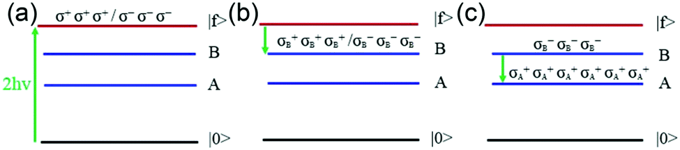 | ||
| Fig. 4 Schematic diagram of two-photon absorption and stimulated Bose scattering. (a) two-photon absorption, (b) the relaxation of exciton states, and (c) stimulated Bose scattering. | ||
For the A′ exciton, the SCP and OCP also exhibit an ultrafast accumulation as displayed in Fig. 3(c). Similar to the B exciton, Fig. 3(d) shows that the A′ exciton has a negative spin/valley polarization. So, the A′ exciton also obeys the two mechanisms for B exciton dynamics, i.e. two-photon absorption and stimulated Bose scattering, and the Dexter-like intervalley coupling. And the former mechanism also dominates the negative spin/valley polarization of the A′ exciton.32
Table 2 lists the best-fitted parameters for the depolarization dynamics of A, B, and A′ excitons in monolayer WSe2. The A exciton holds a biexponential valley depolarization suggesting a fast and a slow relaxation process with a decay time of 0.19 ps and 105 ps, respectively. The fast relaxation process comes from the ultrafast intervalley electron–hole spin–flip exchange coupling and electron–phonon scattering relaxation channel. And the slow one is due to the existence of trions (charged exciton states formed by a pair of electron and hole in the K valley and an electron in the K′ valley). Trions lead to an unequal filling of the K and K′ valley which results in a long-lived depolarization process. In addition, the fast relaxation process dominates the depolarization of A exciton due to the larger proportion of 77%. For the B exciton, it shows a mono-exponential depolarization with only one fast decay process. The fast decay process corresponds to the recombination and relaxation of exciton to the dark states. In contrast, similar to the A exciton, the A′ exciton also shows a biexponential decay valley depolarization dynamics. The proportions of fast and slow relaxation process are also close to those of the A exciton. Due to the interlayer and intralayer effects, the p-orbital of the Se atom perturbs the d-orbital electron band of the W atom (that is, the intralayer effect plays a major role). This causes the splitting of the ground and excited energy levels corresponding to the A exciton transition, resulting in the A′ exciton transition. Therefore, A exciton have similar valley depolarization dynamics to the A′ exciton.
![[thin space (1/6-em)]](https://www.rsc.org/images/entities/char_2009.gif) (−t/τi)
(−t/τi)
| τ 1 (ps) (%) | τ 2 (ps) (%) | |
|---|---|---|
| A exciton | 0.19 ± 0.02 (77) | 105 (23) |
| B exciton | 0.05 ± 0.02 | |
| A′ exciton | 0.08 ± 0.01 (71) | 12 (29) |
Next, we investigate how the vdW heterojunction affects the valley polarization dynamics of WSe2. Fig. 5 shows the SCP and OCP TA spectra of the WSe2/graphene vdW heterojunction at different pump fluences (delay time ∼0.4 ps). Similar to the monolayer WSe2, A exciton has a larger ΔODSCP than ΔODOCP and thus a positive spin/valley polarization while the valley polarizations of B and A′ excitons are negative due to their smaller ΔODSCP compared with ΔODOCP, which is caused by the two-photon absorption and stimulated Bose scattering, and Dexter-like intervalley coupling. Again, the former one dominates the negative polarization because the spin/valley polarization of each exciton exhibits power-dependent characteristics as shown in Table 3.
 | ||
| Fig. 5 The SCP and OCP TA spectra of WSe2/graphene heterojunction (delay time ∼0.4 ps) with pump fluence of (a) 4.85 μJ cm−2, (b) 1.70 μJ cm−2, (c) 0.70 μJ cm−2, (d) 0.24 μJ cm−2, respectively. | ||
(−t/τi)
| Pump fluence (μJ cm−2) | A exciton | B exciton | A′ exciton |
|---|---|---|---|
| 4.85 | 0.13 | −0.19 | −0.98 |
| 1.70 | 0.11 | −0.09 | −0.35 |
| 0.70 | 0.09 | −0.08 | −0.19 |
| 0.24 | 0.01 | −0.05 | 0 |
We also investigate the depolarization dynamics in the WSe2/graphene vdW heterojunction. Here, we take the A exciton as an example. As shown in Fig. 6, the valley polarization of monolayer WSe2 will drop to 0.1 after a very fast decay, and then it will not completely drop to 0 until 150 ps after a long decay. However, in the WSe2/graphene vdW heterojunction, the spin/valley polarization will directly drop to 0 after a very fast decay. We also obtain the decay time of the A exciton in the two structures as listed in Table 4. According to the previous discussion, the A exciton in monolayer WSe2 exhibits a biexponential decay depolarization suggesting a fast and a slow relaxation process. In contrast, the valley depolarization process of the WSe2/graphene vdW heterojunction only has a fast relaxation process. According to our DFT calculations and PL spectra comparison, the excited electrons in WSe2 is expected to be extracted by graphene. This will lead to a reduction of the electron density in WSe2, and then prevent the formation of trions. As mentioned above, the slow relaxation process corresponds to the recombination and relaxation of the trions. That's why the depolarization process in a WSe2/graphene vdW heterojunction only shows a fast decay. In a word, graphene does not affect the ultrafast intervalley electron–hole spin–flip exchange coupling and the electron–phonon scattering relaxation process of monolayer WSe2. But it will destroy the formation of trions in monolayer WSe2, thereby further influencing the depolarization process of monolayer WSe2.
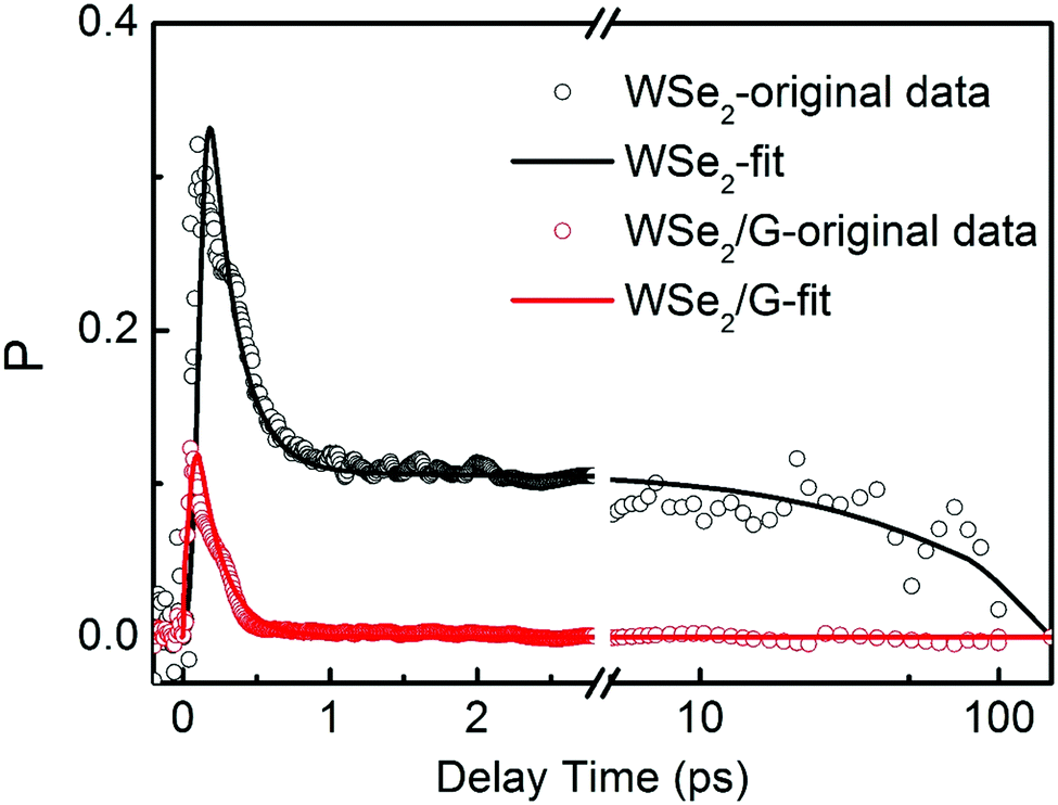 | ||
| Fig. 6 Spin/valley polarization P of the A exciton at different delay times in monolayer WSe2 and the WSe2/graphene heterojunction. | ||
(−t/τi)
| τ 1 (ps) (%) | τ 2 (ps) (%) | |
|---|---|---|
| Monolayer WSe2 | 0.19 ± 0.02 (77) | 105 (23) |
| WSe2/graphene heterojunction | 0.17 ± 0.01 | — |
Conclusions
By circularly polarized ultrafast spectroscopy, we investigate the spin/valley depolarization dynamics of A, B and A′ excitons in monolayer WSe2 as well as its vdW heterojunction with monolayer graphene. The spin/valley polarization of these excitons exhibit a positive correlation with pump fluence. For the depolarization dynamics, the A exciton shows a biexponential decay with a fast and a show relaxation process. The fast relaxation process is due to the ultrafast intervalley electron–hole spin–flip exchange coupling and the electron–phonon scattering relaxation channel. The slow relaxation process is due to the recombination and relaxation of the trion states. Due to the electron extraction effect of graphene, the slow relaxation will disappear and result in a single fast mono-exponential decay in the WSe2/graphene vdW heterojunction. B and A′ excitons have a negative spin/valley polarization which may be mainly due to the two-photon absorption and excited Bose scattering. These results have great significance for understanding the ultrafast spin accumulation and relaxation processes in layered TMDC materials. In order to realize the fabrication of spin/valleytronic devices based on TMDCs, we also need to know how to manipulate excitons dynamics. Up to now, tuning of exciton dynamics by applying stress in 2D TMDCs and their vdW heterojunctions have been achieved.33–36Materials and methods
Circularly polarized femtosecond pump–probe system setup37,38
In all TA experiments, a circularly polarized femtosecond transient absorption system was used to detect monolayer WSe2 and WSe2/graphene heterojunction samples. First, the 800 nm pump pulse with a frequency of 250 Hz is divided into two beams. The beam with higher energy is incident on the TOPAS to generate an excitation light of 740 nm. The excitation light passes through a chopper with a frequency of 125 Hz, and the frequency is changed to 125 Hz. The attenuator can adjust the pump fluence; the beam with lower energy is used to generate the probe light, and sapphire is used as the medium to generate the probe white light in the experiment, thereby generating a broadband probe spectrum of 450–800 nm. We add a Glan prism and a Quarter-Wave Plate in front of the sample in the pump light path, so that the pump light becomes circularly polarized; we add a Glan prism in front of the sample in the probe light path, and a Wollaston prism and a Quarter-Wave Plate behind the sample. A Wollaston prism can generate two separate linearly polarized light beams whose vibration directions are perpendicular to each other. Finally, two spectrometers are used for simultaneous detection, so that the SCP and OCP ultrafast spectra can be obtained at the same time. All the above experiments were performed at room temperature.First-principles calculations
The first-principles calculations based on density functional theory are implemented by the commercial software VASP.39 The projector augmented wave pseudopotential is used to describe the electron–ion interaction.40 The electronic exchange–correlation interaction was described by the generalized gradient approximation (GGA) with the Perdew–Burke–Ernzerhof (PBE) functional.41 The in-plane lattice parameters of optimized hexagonal unit cells (with a 20 Å vacuum layer in the c direction) of monolayer WSe2 and graphene are a = b = 3.32 Å, and a = b = 2.46 Å, respectively. When building the WSe2/graphene heterojunction structure, we choose the 3 × 3 × 1 supercell of monolayer WSe2 and the 4 × 4 × 1 supercell of monolayer graphene to achieve the lowest lattice mismatch and combine them together along the out-of-plane direction. We also consider the vdW interaction by using the Grimme's DFT-D2 scheme.42 The interlayer spacing is determined by the energy minimum. In the structure optimization and band structure calculation of the WSe2/graphene vdW heterojunction, we choose the plane wave cutoff energy to be 520 eV and the K point to be 2 × 2 × 1.Conflicts of interest
There are no conflicts to declare.Acknowledgements
This work was supported by the National Natural Science Foundation of China (NSFC) under Grants 22073037, 21773087, 21603083, 61927814 and 21903035.References
- G. Fiori, F. Bonaccorso, G. Iannaccone, T. Palacios, D. Neumaier, A. Seabaugh, S. K. Banerjee and L. Colombo, Electronics based on two-dimensional materials, Nat. Nanotechnol., 2014, 9, 768–779 CrossRef CAS PubMed.
- P. M. Williams, Photo emission studies of materials with layered structures, Opt. Elect. Prop., 1976, 4, 273 CAS.
- Q. H. Wang, K. Kalantar-Zadeh, A. Kis, J. N. Coleman and M. S. Strano, Electronics and optoelectronics of two-dimensional transition metal dichalcogenides, Nat. Nanotechnol., 2012, 7, 699 CrossRef CAS PubMed.
- D. Jariwala, V. K. Sangwan, L. J. Lauhon, T. J. Marks and M. C. Hersam, Emerging device applications for semiconducting two-dimensional transition metal dichalcogenides, ACS Nano, 2014, 8, 1102 CrossRef CAS PubMed.
- K. F. Mak and J. Shan, Photonics and optoelectronics of 2D semiconductor transition metal dichalcogenides, Nat. Photonics, 2016, 10, 216 CrossRef CAS.
- F. Koppens, T. Mueller, P. Avouris, A. C. Ferrari, M. S. Vitiello and M. Polini, Photodetectors based on graphene, other two-dimensional materials and hybrid systems, Nat. Nanotechnol., 2014, 9, 780 CrossRef CAS PubMed.
- K. F. Mak, C. Lee, J. Hone, J. Shan and T. F. Heinz, Atomically thin MoS2: a new direct-gap semiconductor, Phys. Rev. Lett., 2010, 105, 2 CrossRef PubMed.
- D. Xiao, W. Yao and Q. Niu, Valley-contrasting physics in graphene: Magnetic moment and topological transport, Phys. Rev. Lett., 2007, 99, 236809 CrossRef PubMed.
- H. Zeng, J. Dai, W. Yao, D. Xiao and X. Cui, Valley polarization in MoS2 monolayers by optical pumping, Nat. Nanotechnol., 2007, 7, 490 CrossRef PubMed.
- D. Xiao, G. Liu, W. Feng, X. Xu and W. Yao, Coupled spin and valley physics in monolayers of MoS2 and other group-VI dichalcogenides, Phys. Rev. Lett., 2012, 108, 196802 CrossRef PubMed.
- K. F. Mak, K. L. Mcgill, J. Park and P. L. Mceuen, The valley Hall effect in MoS2 transistors, Science, 2014, 344, 1489 CrossRef CAS PubMed.
- K. S. Novoselov, A. K. Geim, S. V. Morozov, D. Jiang, Y. Zhang, S. V. Dubonos, I. V. Grigorieva and A. A. Firsov, Electric field effect in atomically thin carbon films, Science, 2004, 306, 666 CrossRef CAS PubMed.
- L. Banszerus, M. Schmitz, S. Engels, M. Goldsche, K. Watanabe, T. Taniguchi, B. Beschoten and C. Stampfer, Ballistic transport exceeding 28 μm in CVD grown graphene, Nano Lett., 2016, 16, 1387 CrossRef CAS PubMed.
- M. Drögeler, C. Franzen, F. Volmer, T. Pohlmann, L. Banszerus, M. Wolter, K. Watanabe, T. Taniguchi, C. Stampfer and B. Beschoten, Spin lifetimes exceeding 12 ns in graphene nonlocal spin valve devices, Nano Lett., 2016, 16, 3533 CrossRef PubMed.
- Z. Wang, D. Ki, H. Chen, H. Berger, A. H. MacDonald and A. F. Morpurgo, Strong interface-induced spin-orbit interaction in graphene on WS2, Nat. Commun., 2015, 6, 8339 CrossRef CAS PubMed.
- Z. Wang, D. K. Ki, J. Y. Khoo, D. Mauro, H. Berger, L. S. Levitov and A. F. Morpurgo, Origin and magnitude of ‘designer’ spin-orbit interaction in graphene on semiconducting transition metal dichalcogenides, Phys. Rev. X, 2016, 6, 041020 Search PubMed.
- B. Yang, M. F. Tu, J. Kim, Y. Wu, H. Wang, J. Alicea, R. Q. Wu, M. Bockrath and J. Shi, Tunable spin–orbit coupling and symmetry-protected edge states in graphene/WS2, 2D Mater., 2016, 3, 031012 CrossRef.
- B. Yang, M. Lohmann, D. Barroso, I. Liao, Z. S. Lin, Y. W. Liu, L. Bartels, K. Watanabe, T. Taniguchi and J. Shi, Strong electron-hole symmetric Rashba spin-orbit coupling in graphene/monolayer transition metal dichalcogenide heterostructures, Phys. Rev. B, 2017, 96, 041409 CrossRef.
- M. Gmitra and J. Fabian, Graphene on transition-metal dichalcogenides: A platform for proximity spin-orbit physics and optospintronics, Phys. Rev. B: Condens. Matter Mater. Phys., 2015, 92, 155403 CrossRef.
- B. Yang, M. Everardo, K. Jeongwoo, D. Barroso, M. Lohmann, Y. W. Liu, Y. D. Xu, R. Q. Wu, L. Bartels, K. Watanabe, T. Taniguchi and J. Shi, Effect of distance on photoluminescence quenching and proximity-induced spin-orbit coupling in graphene/WSe2 heterostructures, Nano Lett., 2018, 18, 3580 CrossRef CAS PubMed.
- W. Yan, O. Txoperena, R. Llopis, H. Dery, L. E. Hueso and F. Casanova, A two-dimensional spin field-effect switch, Nat. Commun., 2016, 7, 13372 CrossRef CAS PubMed.
- A. Dankert and S. P. Dash, Electrical gate control of spin current in van der Waals heterostructures at room temperature, Nat. Commun., 2017, 8, 16093 CrossRef CAS PubMed.
- M. Gmitra and J. Fabian, Graphene on transition-metal dichalcogenides: A platform for proximity spin-orbit physics and optospintronics, Phys. Rev. B: Condens. Matter Mater. Phys., 2015, 92, 155403 CrossRef.
- Y. K. Luo, J. Xu, T. Zhu, G. Wu, E. J. McCormick, W. Zhan, M. R. Neupane and R. K. Kawakami, Opto-valleytronic spin injection in monolayer MoS2/few-layer graphene hybrid spin valves, Nano Lett., 2017, 17, 3877 CrossRef CAS PubMed.
- J. Ye, Y. Li, T. Yan, G. H. Zhai and X. H. Zhang, Ultrafast dynamics of spin generation and relaxation in layered WSe2, J. Phys. Chem. Lett., 2019, 10, 2963 CrossRef CAS PubMed.
- Z. Wang, L. Zhao, K. F. Mak and J. Shan, Probing the spin-polarized electronic band structure in monolayer transition metal dichalcogenides by optical spectroscopy, Nano Lett., 2017, 17, 740 CrossRef CAS PubMed.
- M. Manca, M. M. Glazov, C. Robert, F. Cadiz, T. Taniguchi, K. Watanabe, E. Courtade, T. Amand, P. Renucci, X. Marie, G. Wang and B. Urbaszek, Enabling valley selective exciton scattering in monolayer WSe2 through upconversion, Nat. Commun., 2017, 8, 14927 CrossRef CAS PubMed.
- R. Schmidt, G. Berghäuser, R. Schneider, M. Selig, P. Tonndorf, E. Malic, A. Knorr, S. M. de Vasconcellos and R. Bratschitsch, Ultrafast Coulomb-induced intervalley coupling in atomically thin WS2, Nano Lett., 2016, 16, 2945 CrossRef CAS PubMed.
- G. Berghäuser, I. Bernal-Villamil, R. Schmidt, R. Schneider, I. Niehues, P. Erhart, S. M. de Vasconcellos, R. Bratschitsch, A. Knorr and E. Malic, Inverted valley polarization in optically excited transition metal dichalcogenides, Nat. Commun., 2018, 9, 971 CrossRef PubMed.
- A. Molina-SáNchez, D. Sangalli, L. Wirtz and A. Marini, Ab initio calculations of ultrashort carrier dynamics in two-dimensional materials: valley depolarization in single-layer WSe2, Nano Lett., 2017, 17, 4549 CrossRef PubMed.
- Z. Wang, A. Molina-Sánchez, P. Altmann, D. Sangalli, D. De Fazio, G. Soavi, U. Sassi, F. Sassi, F. Ciccacci, M. Finazzi, L. Wirtz, A. C. Ferrari, A. Marini, G. Cerullo and S. Dal Conte, Intravalley spin-flip relaxation dynamics in single-layer WS2, Nano Lett., 2018, 18, 6882 CrossRef CAS PubMed.
- W. Zhao, Z. Ghorannevis, L. Chu, M. L. Toh, C. Kloc, P. H. Tan and G. Eda, Evolution of electronic structure in atomically thin sheets of WS2 and WSe2, ACS Nano, 2013, 7, 791 CrossRef CAS PubMed.
- W. Zhao, E. C. Regan, D. Wang, C. Jin, S. Hsieh, Z. Wang, J. Wang, Z. Wang, K. Yumigeta, M. Blei, K. Watanabe, T. Taniguchi, S. Tongay, N. Y. Yao and F. Wang, Dynamic tuning of Moiré excitons in a WSe2/WS2 heterostructure via mechanical deformation, Nano Lett., 2021, 21, 8910 CrossRef CAS PubMed.
- H. Li, Y. Qin, B. Ko, D. B. Trivedi, D. Hajra, M. Y. Sayyad, L. Liu, S. H. Shim, H. Zhuang and S. Tongay, Anomalous behavior of 2D Janus excitonic layers under extreme pressures, Adv. Mater., 2020, 32, 2002401 CrossRef CAS PubMed.
- F. Ersan and S. Sarikurt, Monitoring the electronic, thermal and optical properties of two-dimensional MoO2 under strain via vibrational spectroscopies: a first-principles investigation, Phys. Chem. Chem. Phys., 2019, 21, 19904 RSC.
- D. Li, H. Shan, C. Rupprecht, H. Knopf, K. Watanabe, T. Taniguchi, Y. Qin, S. Tongay, M. Nuß, S. Schröder, F. Eilenberger, S. Höfling, C. Schneider and T. Brixner, Hybridized exciton-photon-phonon states in a transition metal dichalcogenide van der Waals heterostructure microcavity, Phys. Rev. Lett., 2022, 128, 087401 CrossRef CAS PubMed.
- X. Chen, Z. Wang, L. Wang, H. Y. Wang, Y. Y. Yue, H. Wang, X. P. Wang, A. T. S. Wee, C. W. Qiu and H. B. Sun, Investigating the dynamics of excitons in monolayer WSe2 before and after organic super acid treatment, Nanoscale, 2018, 10, 9346 RSC.
- X. Chen, L. Wang, H. Y. Wang, X. P. Wang, Y. Luo and H. B. Sun, Electronic structure evolution and exciton energy shifting dynamics in WSe2: from monolayer to bulk, J. Phys. D: Appl. Phys., 2021, 54, 354002 CrossRef CAS.
- G. Kresse and J. Furthmüller, Efficient iterative schemes for ab initio total-energy calculations using a plane-wave basis set, Phys. Rev. B: Condens. Matter Mater. Phys., 1996, 54, 11169 CrossRef CAS PubMed.
- P. E. Blöchl, Projector augmented-wave method, Phys. Rev. B: Condens. Matter Mater. Phys., 1994, 50, 17953 CrossRef PubMed.
- J. P. Perdew, K. Burke and M. Ernzerhof, Generalized Gradient Approximation Made Simple, Phys. Rev. Lett., 1996, 77, 3856 CrossRef PubMed.
- S. Grimme, Semiempirical GGA-type density functional constructed with a long-range dispersion correction, J. Comput. Chem., 2006, 27, 1787 CrossRef CAS PubMed.
| This journal is © the Owner Societies 2022 |