
 Open Access Article
 This Open Access Article is licensed under a
 Creative Commons Attribution 3.0 Unported Licence
Stress induced delamination of suspended MoS2 in aqueous environments†
Michal
Macha
*,
Mukeshchand
Thakur
,
Aleksandra
Radenovic
 * and
Sanjin
Marion‡
*
* and
Sanjin
Marion‡
*
Ecole Polytechnique Federale de Lausanne (EPFL), Lausanne, Switzerland. E-mail: michal.macha@epfl.ch; aleksandra.radenovic@epfl.ch; sanjin.marion@imec.be
First published on 29th July 2022
Abstract
Applying hydrostatic pressure with suspended 2D material thin membranes allows probing the effects of lateral strain on the ion and fluid transport through nanopores. We demonstrate how both permanent and temporary delamination of 2D materials can be induced by pressure and potential differences between the membrane, causing a strong mechanosensitive modulation of ion transport. Our methodology is based on in situ measurements of ionic current and streaming modulation as the supporting membrane is indented or bulged with pressure. We demonstrate how indirect measurements of fluid transport through delaminated MoS2 membranes is achieved through monitoring streaming current and potential. This is combined with TEM images of 2D material membranes before and after aqueous measurements, showing temporary delamination during mechanical or electrical stress. The obtained results allow a better understanding of measurements with supported 2D materials, i.e. avoiding misinterpreting measured data, and could be used to probe how the electrical field and fluid flow at the nanoscale influence the adhesion of supported 2D materials.
Introduction
The unique properties of atomic thickness, mechanical and electric properties1–6 as well as rapid advancements in 2D materials synthesis methods7,8 have made 2D-material-based devices a platform of choice to study nanoscale physics in aqueous environments.9 Suspended, nanoporous 2D-membranes are used in applications such as biosensing,10 DNA translocation,11 osmotic energy harvesting,12–14 water desalination15 and gas filtration.16 In most nanofluidic experiments, the application of electrical fields is used as a basic tool to probe the ion transport properties of the system.17,18 Lately however, the use of hydrostatic pressure as an additional probe has been found to be critically important to study the nonlinear coupling of ion transport with fluid flow19,20 as well as a tool to probe proper wetting behaviour.21It has been established, that applying high voltage can be potentially damaging to the 2D material as it can cause membrane breakdown11,22 and delamination through electrolyte intercalation.23,24 Even though the strain-induced wrinkling and delamination was thoroughly studied,25–27 it is not fully explored how applying hydrostatic pressure can influence the membrane performance and 2D film adhesion to the substrate in an aqueous environment. It was shown, that surface-related phenomena such as material damage, delamination or nanobubbles28 can exhibit nonlinear current signals,20,21,23 analogous to those reported as ionic coulomb blockade.29 Thus, even though MoS2 was proven stable at working pressure of up to 3.5 bar,20,30 further investigation of the application of both electrical fields and pressure is crucial to uncover adhesion-related artifacts, help understand the 2D-nanofluidic system and bring insights into designing an artifact-free 2D-material platforms.
In this work we are using a symmetrical hydraulic pressure based setup (i.e. with the pressure applied to the backside, frontside or both sides of the membrane simultaneously) to investigate the MoS2/membrane adhesion behaviour during nanofluidic experiments.20,21 We investigate the influence of applying high voltages (including voltage-mediated pore-drilling protocols) on the reversible 2D film delamination. We demonstrate how the membrane deformation through applied hydrostatic pressure can lead to adhesion defects such as MoS2 wrinkling and flapping manifested through extremely non-linear current signals and unstable streaming currents. With transmission electron microscopy (TEM) images taken before and after the measurements we showcase the reversibility of the delamination processes. Finally, by analyzing the asymmetric and unstable system behaviour under pressure we show how to properly identify and study membrane properties. The experimental methodology presented here enables to uncover the adhesion issues and brings a deeper understanding of nanoscale physics of suspended atomically thin films in aqueous solutions and their ion transport behavior under experimental stimuli.
Results and discussion
Voltage-driven delamination of MoS2
We have used an atomically thin MoS2 membrane, irradiated with Xe ions and suspended over the Si/SiN aperture (see Materials and methods section) to probe the adhesion properties in an electrolyte solution. The MoS2 membrane was placed in the flowcell adapted to apply pressure gradients and test wetting of nanopores20,21 (Fig. 1A). Degassed 1 M potassium chloride (KCl) solution was used as an electrolyte on both cis- and trans-sides of the MoS2. A typical experiment with freestanding MoS2 membranes starts with probing the membrane conductance with voltage sweeps and ensuring proper wetting of the system through the application of hydrostatic pressure (i.e. achieving stable values of membrane resistance and capacitance expected of monolayer MoS2 suspended over the Si/SiN aperture21). Our wetting protocol involves flushing with a degassed electrolyte solution and applying hydrostatic pressure to both sides of the membrane (i.e. compression pressure) to reabsorb any potential, obstinate vapor bubbles back into the solution as reported previously.21 | ||
| Fig. 1 Temporary delamination of MoS2 during nanofluidic measurements. (A) Schematic description of the measurement geometry with a TEM image of suspended MoS2 and the corresponding FFT. The experimental setup and details match those described in ref. 20 and 21, including the transfer method for MoS2 and pressure setup schematics. (B) Measured values of the ionic current (blue, left axis) and applied potential difference (red, right axis) on a MoS2 sample versus time. Panels C and D show the same substrate as in panel A imaged after the ionic measurement in liquid (panel B), indicating that the MoS2 has survived the liquid immersion and measurement, and the presence of a “flap” near the aperture (panel C). In the proposed model, applied high voltage (or pressure) can cause intermittent delamination of MoS2 leading to ionic conduction through a created fluidic pathway (E). | ||
In situ nanopore creation is the crucial step of substrate preparation which can compromise the sample membrane. We have observed that this step, often regarded as robust and facile, can introduce crucial MoS2 delamination issues. The most commonly used method is the electrochemical reaction (ECR) drilling protocol.11,17,31 A methodology widely used in the nanopore research field to create pores in situ by applying gradually increasing high electric fields.22 A constant or periodic application of high potential differences between the two sides of the membrane is expected to cause defect expansion through an ECR and eventually form a nanopore of controlled dimensions.11,22 In an attempt to use high voltages to produce nanopores from pristine monolayer MoS2 membranes, we have applied voltages up to several volts. In some cases, we noted that after such applications, the resistance of the sample would afterward return to its original value. An example of such a measurement with a pristine MoS2 membrane is shown in Fig. 1B. Typically, the ECR and subsequent MoS2 pore formation is expected to start occurring at applied voltages as low as 0.75 V in MoS2,11 with drilling protocols reported up to 7 V for graphene.31 Higher voltages are in general expected to increase the probability of drilling a pore in ultrathin membranes.22 In our case, we applied potential differences as high as 7 V and after comparing the substrate before and after experiments in TEM (Fig. 1C and D) we found not only that the intact MoS2 surface has survived the ECR drilling protocol, but also a presence of a folded layer in close vicinity to the suspended area (Fig. 1C) indicating that the MoS2 has shifted in its placement on the substrate.
As observed previously in graphene, applying a high electric field can cause direct membrane delamination from the substrate23 which can impact membrane conductance (Fig. 1E). Such a loss in adhesion was found to occur after exceeding a threshold transmembrane voltage of 0.25–0.5 V depending on factors such as 2D film surface roughness, existing defects or surface folds.23 The process was found to be reversible i.e. delaminated 2D material relaminates after the transmembrane potential difference is removed and the electrolyte intercalation between 2D film and substrate is no longer energetically favorable.23 A possible mechanism used in the literature for similar effects would involve local Joule heating at the pore causing liquid superheating producing explosive nucleation of a vapor bubble.32,33 In our case MoS2 delamination via local bubbling on the MoS2/SiN interface is unlikely as we use an electrolyte solution that is undersaturated with gas and the starting ionic current through the pore is too small to induce significant Joule heating. On the other side, ionic-current induced pore enlargement is also not anticipated as it is reported to occur at low- and moderate applied electric fields and would cause permanent pore etching.34 We do confirm the delamination hypothesis by observing the reversible increase in ionic conductance while applying high voltage and measuring a nonlinear IV curve shape (Fig. S1, ESI†). This is in accordance to reported studies of voltage-driven graphene delamination23 triggered by an electric force. We provide additional proof with TEM images showcasing the survival of intact suspended MoS2 after the experiment (Fig. 1E). We hypothesize a forming of a reversible conductive pathway through locally delaminated MoS2 (Fig. 1E) which then collapses back when there is no external stimuli.
Pressure driven, irreversible delamination of MoS2
We have observed that delamination may in some cases occur without high voltages but with applying pressure from the backside of the membrane (causing membrane bulging). We see the opening of a conductive channel in the membrane manifested through rapid increase in conductance as the pressure crosses a critical value due to the membrane being bulged (see Fig. S2, ESI†). The intact character of suspended MoS2 area is seen with multiple samples imaged post-experiment (see Fig. S3, ESI†), indicating liftoff of the MoS2 monolayer from the substrate and subsequent reattachment after removing from the flowcell environment (see Materials and methods section). The exact pressure value at which delamination happens varying from sample to sample (ranging from approx. 2–3 bar for 20 nm thick SiN membranes with square window sizes of 20 μm by 20 μm). The possible cause may be the difference between the MoS2 monolayer film area (i.e. the size of a MoS2 single crystal) transferred over the SiN aperture, varying between substrates, and batch-to-batch differences in the roughness of SiN surface.35 This is an inherent issue with currently used state-of-art thin film transfer techniques. The normal force on the suspended MoS2 can be estimated from the diameter of the pore of d = 60 nm to be about 1.5 nN at 3 bar of pressure. This pressure causes a force that is an order of magnitude smaller than typical forces applied in mechanical indentation experiments with atomic force microscopy30,36 and is not expected to compromise the mechanical stability of the suspended film. We conclude that hydrostatic pressure applied from the backside can therefore lift-off the MoS2 – causing in situ delamination with possible subsequent reattachment of the 2D material to the surface in a different condition (i.e. after removing the substrate from aqueous solution).Pressure driven, reversible delamination of MoS2
Interestingly, the same pressure applied from the membrane's backside does not yield symmetrical results when we reverse its directionality. MoS2/SiN delamination events are also present while applying pressure from the frontside of the membrane (i.e. causing membrane indentation), albeit different and reversible in character (Fig. 2). In comparison to MoS2 indentation experiments37 and bulging/indentation experiments with graphene38–40 this is not expected to cause delamination. In our case, we believe that the possible cause could be linked to substrate induced, local wrinkling. This effect has been seen in materials where the underlying substrate was compressed,41–43 where the 2D material locally detaches as it is energetically more favorable to loose adhesion than to conform to the deforming substrate curvature.35 We can further characterize the behaviour seen in Fig. 2 by doing streaming current and voltage measurements (Fig. 3 and 4). Streaming current measurements indicate the presence of liquid flow between the two sides of the membrane when the membrane is in a bulged state (Fig. 3a) most likely due to water permeating between the 2D material and the substrate, but in the indented state a streaming pathway is opened up a critical pressure is applied (≈2–3 bar, Fig. 3b). This critical pressure matches qualitatively the pressure values seen in ionic current measurements (Fig. 2b and c) and indicates an abrupt and temporary opening of a large pathway for fluid flow between the two sides of the membrane.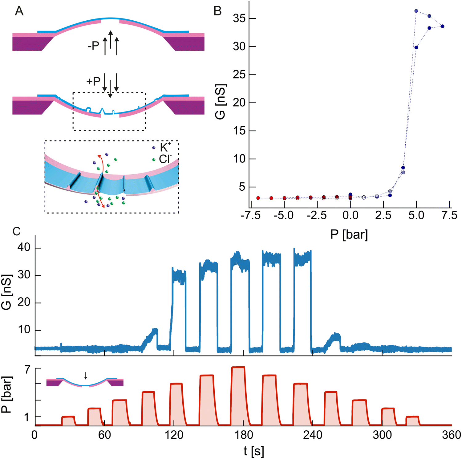 | ||
| Fig. 2 Delamination of suspended MoS2 due to pressure induced surface indentation. (A) Toy model demonstrating bulging (top) and indentation (bottom) of the membrane under positive and negative hydraulic pressure gradients. The bottom inset shows the proposed mechanism for the formation of conductive channels between two sides of the membrane due to local wrinkling and detachment of the MoS2. (B) Conductance G of the sample was obtained through ionic current measurements at 100 mV at different values of the pressure gradient P applied to the membrane. The measurement protocol involved subsequent measurements at different pressure values followed by a measurement at P = 0 bar to confirm that the baseline value has not changed. Panel (C) shows the time traces of the pressure P and conductance G as shown in panel b. Note that only positive pressure gradient values are shown to emphasize the abrupt increase in conductance seen in panel B. | ||
 | ||
| Fig. 3 Streaming measurements on suspended MoS2 during delamination. (A) Streaming current Is as measured on the sample shown in Fig. 2b and c during the membrane bulging state. No external potential was applied to the sample (closed circuit measurement). (B) Anomalous increase of streaming current Is for positive pressures matching the delaminating state in Fig. 2b and c. The top panel show the time trace of the measured streaming current Is, while the bottom panel shows the applied pressure gradient P. | ||
 | ||
| Fig. 4 Streaming measurements on suspended MoS2 during delamination. (A) Streaming potential VS measurements obtained for four different samples showing analogous behaviour as in Fig. 2b and c. Measurements were done in the open circuit configuration. A linear fit gives the values of the apparent zeta potential for the membrane. (Note that the measurement protocol follows the same approach as before with intermediary measurements at P = 0 to check for baseline drift, and two measurements at each intermediary pressure value to check for hysteresis after the maximal pressure value was applied) Time traces of the streaming potential VS and applied pressure gradient for Sample 1 are shown in panels B and C. Panel (B) shows measurements of the streaming potential during the bulging case, while panel C during the delaminating case. | ||
In order to clarify the nature of the ion transport, we opted to perform streaming potential measurements (Fig. 4c) using an electrometer grade buffer preamplifier. Streaming potential, unlike streaming current, does not in the first approximation depend on the effective size of the ionic channel (i.e. the geometry), and can be written as VS = εrε0ζP/(ση) with εr the relative permittivity of water, ε0 the permittivity of vacuum, ζ the surface zeta potential, P the pressure gradient, σ the electrolyte solution conductivity and η the viscosity of the solution.21,44,45 In four samples showing the same qualitative behaviour as presented here we obtain comparable results i.e. reversible, local delamination or loss in adhesion that is caused directly by measurement conditions (high voltage or applied pressure). The reversible, impermanent character of this state is confirmed by comparing TEM images before and after measurements (see Fig. S4, ESI†). In the bulging case we note the presence of a streaming potential with zeta potential values ranging from 11 to 17 mV, typical for MoS2 pores and higher than the usual value of 8–9 mV we see in these conditions without any MoS2 present (pristine SiNx). This would indicate an occurrence of a water flowing through the MoS2 membrane and dragging solute ions in the surface double layer while in an indented/wrinkled state, possibly either through defects in the MoS2 or through a channel formed due to the normal force of the pressure lifting the MoS2 away from the aperture. The streaming potential in the indented case shows unstable and almost an order of magnitude larger values as pressure is applied. The pressure sweep protocol used in this work assumes the application of gradually increasing hydrostatic pressure with a pause at 0 bar in between the pressure steps (Fig. 4B and C). The observed, unstable variations in measured streaming potential do occur at each application of the pressure. This could suggest pressure-induced changes to MoS2 surface charges due to wrinkling – ion-conducting-wrinkle pathways changing and reshaping under each application of a hydrostatic pressure step.
Conclusion
The use of pressure with suspended 2D materials on a thin membrane substrate is of interest as it allows probing the effects of lateral strain on the ion transport of nanopores in 2D materials20,46 as well as coupling of ion transport with fluid flow.19,20 Both these effects require a good understanding of the behaviour of such systems under mechanical and electrical strain. This work demonstrates how both permanent and temporary delamination of 2D materials can be induced by pressure and potential differences between the membrane. We demonstrate that the application of pressure pulses can change the adhesion and shape of delaminated 2D film wrinkles leading to unstable surface charges resulting in unexpected transmembrane streaming currents. We show a measurement methodology that allows to detect these adhesion issues and accurately identify them. The suspended 2D film wrinkling phenomenon needs to be taken into consideration while using pressure probes for wetting, bubble gating through applied hydrostatic pressure21 and probing ionic properties using pressurized setups.20,30,47 Although the large modulation of ionic transport due to partial delamination is similar to the case of pressure induced nanoparticle blockages47 and could be used to produce more robust mechanical pressure sensors, it is still far away from true mechanosensitivity where ion transport is modulated by mechanical stress directly modulating the energy barriers for single ion translocations.46,48 Our approach allows a better understanding of measurements with supported 2D materials, i.e. avoiding misinterpreting the measured data and could be used to probe how the electrical field and fluid flow at the nanoscale would influence membrane adhesion. Given the dynamic and volatile nature of the delamination events, the design and fabrication of nanofluidic devices with supported 2D films has to be revised to ensure stable and reliable device performance.Methods
Substrate preparation MoS2 was synthesized on a 3-inch sapphire substrate with a tube-furnace MOCVD setup using the liquid-promoter approach.49,50 Cleaned and annealed in air sapphire wafers were coated with sodium molybdate mixture and heated to 870 °C under ambient argon flow. After reaching the designated temperature the substrate was subjected to the flow of 12 sccm of molybdenum hexacarbonyl (MoCO6), 4 sccm of diethyl sulfide (DES), 4 sccm of hydrogen and 1 sccm of oxygen for 30 min. Synthesized MoS2 on sapphire was then cooled naturally under argon atmosphere. As-grown monolayer MoS2 was transferred onto holey Si/SiN membrane chips (Norcada) using wet transfer method17,49 and imaged in the transmission electron microscope (TEM) to confirm the successful fabrication of a suspended MoS2 membrane.TEM imaging Before and after nanofluidic experiments suspended MoS2 membranes were imaged at ThermoFischer Talos F200S at 80 kV accelerating voltage. After the nanofluidic measurement, substrates were taken out of the flowcell and bathed several times in hot DI water to dissolve the remaining salts and minimize subsequent device contamination and salt crystallization. Substrates were then gently dried and imaged. All salt-cleaning steps were performed with caution to minimize the fluid flow and potential MoS2 delamination caused by that.
Nanofluidic measurements Samples used were in the form of 5 × 5 mm Si/SiN membrane devices mounted into a fluidic chamber as described previously and using the same measurement protocols.20,21 All liquids in touch with the sample were in situ degassed using a 925 μl Systec AF degassing chamber. Electrical measurements were done using a Zurich Instruments MFLI lock-in amplifier with the MF-DIG option using chlorinated Ag/Cl electrodes. Both DC and AC bias was applied using the signal output of the instrument, while the current through the sample was measured using the built in current to voltage converter. Streaming potential measurements were performed using an ultra-low input bias current (femtoampere level) electrometer grade buffer using the ADA4530 opamp. All electrical measurements done while sweeping the pressure were done after the pressure level has stabilized to at least 5% of the target value. In the case of DC current measurements, an additional wait time of 1 s was performed after the pressure settling.
We used 1 M KCl with 10 mM Tris buffered to pH 8 for all conductance measurements. All buffers were prepared using MiliQ grade water (18.2 MΩ cm−1). The conductivity of all solutions was checked before use with a Mettler–Toledo FiveEasy Plus. All solutions were filtered through a 20 nm filter before use (Whatman Anotop 25 plus).
Author contributions
A. R., S. M., and M. M. conceived and designed the experiments; M. M. synthesized MoS2, M. T. performed thin film transfer; M. M. did nanofluidic measurements and TEM imaging, M. M. wrote the paper, with inputs from all authors; A. R and S. M. supervised the project; All authors discussed the results and commented on the manuscript.Conflicts of interest
There are no conflicts to declare.Acknowledgements
This work was financially supported by a Swiss National Science Foundation (SNSF) support through 200021_192037 and the CCMX Materials Challenge grant “Large area growth of 2D materials for device integration”. In addition, we are thankful to Norcada for providing substrate chips, A. Smolyanitsky for useful discussions, and the Interdisciplinary Centre for Electron Microscopy (CIME) at EPFL for access to TEMs.References
- G. G. Naumis, Electronic properties of two-dimensional materials, Synth., Model., Charact. 2D Mater., Their Heterostruct., 2020, 77–109, DOI:10.1016/B978-0-12-818475-2.00005-2.
- D. Akinwande, et al., A review on mechanics and mechanical properties of 2D materials—Graphene and beyond, Extreme Mech. Lett., 2017, 13, 42–77, DOI:10.1016/J.EML.2017.01.008.
- B. Radisavljevic, A. Radenovic, J. Brivio, V. Giacometti and A. Kis, Single-layer MoS2 transistors, Nat. Nanotechnol., 2011, 6, 147–150, DOI:10.1038/nnano.2010.279.
- A. Splendiani, et al., Emerging Photoluminescence in Monolayer MoS2, Nano Lett., 2010, 10(4), 1271–1275, DOI:10.1021/NL903868W.
- A. Castellanos-Gomez, et al., Elastic Properties of Freely Suspended MoS2 Nanosheets, Adv. Mater., 2012, 24(6), 772–775, DOI:10.1002/ADMA.201103965.
- J.-W. Jiang, H. S. Park and T. Rabczuk, Molecular dynamics simulations of single-layer molybdenum disulphide (MoS2): Stillinger-Weber parametrization, mechanical properties, and thermal conductivity, J. Appl. Phys., 2013, 114(6), 064307, DOI:10.1063/1.4818414.
- S. Alam, M. Asaduzzaman Chowdhury, A. Shahid, R. Alam and A. Rahim, Synthesis of emerging two-dimensional (2D) materials – Advances, challenges and prospects, FlatChem, 2021, 30, 100305, DOI:10.1016/J.FLATC.2021.100305.
- J. Yu, J. Li, W. Zhang and H. Chang, Synthesis of high quality two-dimensional materials via chemical vapor deposition, Chem. Sci., 2015, 6(12), 6705–6716, 10.1039/C5SC01941A.
- Y. He, M. Tsutsui, Y. Zhou and X. S. Miao, Solid-state nanopore systems: from materials to applications, NPG Asia Mater., 2021, 13(1), 1–26, DOI:10.1038/s41427-021-00313-z.
- J. Lee, et al., Stabilization of graphene nanopore, Proc. Natl. Acad. Sci. U. S. A., 2014, 21, 7522–7526, DOI:10.1073/pnas.1400767111.
- J. Feng, et al., Identification of single nucleotides in MoS2 nanopores, Nat. Nanotechnol., 2015, 10, 1070–1076, DOI:10.1038/nnano.2015.219.
- M. Macha, S. Marion, V. V. Nandigana and A. Radenovic, 2D materials as an emerging platform for nanopore-based power generation, Nat. Rev. Mater., 2019, 4(9), 588–605, DOI:10.1038/s41578-019-0126-z.
- M. Graf, et al., Light-Enhanced Blue Energy Generation Using MoS2 Nanopores, Joule, 2019, 3(6), 1549–1564, DOI:10.1016/j.joule.2019.04.011.
- J. Feng, et al., Observation of ionic Coulomb blockade in nanopores, Nat. Mater., 2016, 15(8), 850–855, DOI:10.1038/nmat4607.
- M. Heiranian, A. B. Farimani and N. R. Aluru, Water desalination with a single-layer MoS 2 nanopore, Nat. Commun., 2015, 6, 1–6, DOI:10.1038/ncomms9616.
- J. P. Thiruraman, et al., Gas flow through atomic-scale apertures, Sci. Adv., 2020, 6(51), eabc7927, DOI:10.1126/sciadv.abc7927.
- M. Graf, Fabrication and practical applications of molybdenum disulfide nanopores, Nat. Protoc., 2019, 14, 1130–1168 CrossRef CAS PubMed.
- D. G. Haywood, A. Saha-Shah, L. A. Baker and S. C. Jacobson, Fundamental Studies of Nanofluidics: Nanopores, Nanochannels, and Nanopipets, Anal. Chem., 2014, 87(1), 172–187, DOI:10.1021/AC504180H.
- A. Marcotte, T. Mouterde, A. Niguès, A. Siria and L. Bocquet, Mechanically activated ionic transport across single-digit carbon nanotubes, Nat. Mater., 2020, 19(10), 1057–1061, DOI:10.1038/s41563-020-0726-4.
- S. J. Davis, et al., Pressure-Induced Enlargement and Ionic Current Rectification in Symmetric Nanopores, Nano Lett., 2020, 20(11), 8089–8095, DOI:10.1021/acs.nanolett.0c03083.
- S. Marion, M. Macha, S. J. Davis, A. Chernev and A. Radenovic, Wetting of nanopores probed with pressure, Phys. Chem. Chem. Phys., 2021, 23(8), 4975–4987, 10.1039/D1CP00253H.
- H. Kwok, K. Briggs and V. Tabard-Cossa, Nanopore fabrication by controlled dielectric breakdown, PLoS One, 2014, e92880, DOI:10.1371/journal.pone.0092880.
- J. Loessberg-Zahl, et al., Exploring Voltage Mediated Delamination of Suspended 2D Materials as a Cause of Commonly Observed Breakdown, J. Phys. Chem. C, 2020, 124(1), 430–435, DOI:10.1021/acs.jpcc.9b08500.
- K. Verguts, J. Coroa, C. Huyghebaert, S. De Gendt and S. Brems, Graphene delamination using ‘electrochemical methods’: an ion intercalation effect, Nanoscale, 2018, 10(12), 5515–5521, 10.1039/C8NR00335A.
- L. Meng, et al., Wrinkle networks in exfoliated multilayer graphene and other layered materials, Carbon, 2020, 156, 24–30, DOI:10.1016/J.CARBON.2019.09.035.
- S. Yang, et al., Tuning the optical, magnetic, and electrical properties of ReSe2 by nanoscale strain engineering, Nano Lett., 2015, 15(3), 1660–1666, DOI:10.1021/nl504276u.
- A. Castellanos-Gomez, et al., Local strain engineering in atomically thin MoS2, Nano Lett., 2013, 13(11), 5361–5366, DOI:10.1021/nl402875m.
- L. Cantley, et al., Voltage gated inter-cation selective ion channels from graphene nanopores, Nanoscale, 2019, 11(20), 9856–9861, 10.1039/C8NR10360G.
- J. Feng, et al., Observation of ionic Coulomb blockade in nanopores, Nat. Mater., 2016, 15(8), 850–855, DOI:10.1038/NMAT4607.
- S. Marion and A. Radenovic, Towards artificial mechanosensing, Nat. Mater., 2020, 19(10), 1043–1044, DOI:10.1038/s41563-020-00811-5.
- A. T. Kuan, B. Lu, P. Xie, T. Szalay and J. A. Golovchenko, Electrical pulse fabrication of graphene nanopores in electrolyte solution, Appl. Phys. Lett., 2015, 106(20), 858–861, DOI:10.1063/1.4921620.
- E. V. Levine, M. M. Burns and J. A. Golovchenko, Nanoscale dynamics of Joule heating and bubble nucleation in a solid-state nanopore, Phys. Rev. E, 2016, 93(1), 013124, DOI:10.1103/PhysRevE.93.013124.
- G. Nagashima, E. V. Levine, D. P. Hoogerheide, M. M. Burns and J. A. Golovchenko, Superheating and homogeneous single bubble nucleation in a solid-state nanopore, Phys. Rev. Lett., 2014, 113(2), 024506, DOI:10.1103/PhysRevLett.113.024506.
- C. Leung, et al., Mechanisms of solid-state nanopore enlargement under electrical stress, Nanotechnology, 2020, 31(44), 44LT01, DOI:10.1088/1361-6528/aba86e.
- S. Deng, E. Gao, Z. Xu and V. Berry, Adhesion Energy of MoS2 Thin Films on Silicon-Based Substrates Determined via the Attributes of a Single MoS2 Wrinkle, ACS Appl. Mater. Interfaces, 2017, 9(8), 7812–7818, DOI:10.1021/acsami.6b16175.
- S. Bertolazzi, J. Brivio and A. Kis, Stretching and breaking of ultrathin MoS2, ACS Nano, 2011, 5(12), 9703–9709, DOI:10.1021/nn203879f.
- K. Liu, et al., Elastic properties of chemical-vapor-deposited monolayer MoS2, WS2, and their bilayer heterostructures, Nano Lett., 2014, 14(9), 5097–5103, DOI:10.1021/NL501793A.
- N. G. Boddeti, et al., Graphene blisters with switchable shapes controlled by pressure and adhesion, Nano Lett., 2013, 13(12), 6216–6221, DOI:10.1021/nl4036324.
- N. G. Boddeti, et al., Mechanics of adhered, pressurized graphene blisters, J. Appl. Mech., 2013, 80(4), 040909, DOI:10.1115/1.4024255/370651.
- S. P. Koenig, N. G. Boddeti, M. L. Dunn and J. S. Bunch, Ultrastrong adhesion of graphene membranes, Nat. Nanotechnol., 2011, 6(9), 543–546, DOI:10.1038/nnano.2011.123.
- D. Vella, J. Bico, A. Boudaoud, B. Roman and P. M. Reis, The macroscopic delamination of thin films from elastic substrates, Proc. Natl. Acad. Sci. U. S. A., 2009, 106(27), 10901–10906, DOI:10.1073/PNAS.0902160106.
- C. Androulidakis, E. N. Koukaras, M. G. Pastore Carbone, M. Hadjinicolaou and C. Galiotis, Wrinkling formation in simply-supported graphenes under tension and compression loadings, Nanoscale, 2017, 9(46), 18180–18188, 10.1039/C7NR06463B.
- C. J. Brennan, et al., Interface Adhesion between 2D Materials and Elastomers Measured by Buckle Delaminations, Adv. Mater. Interfaces, 2015, 2(16), 1500176, DOI:10.1002/ADMI.201500176.
- P. Waduge, et al., Nanopore-Based Measurements of Protein Size, Fluctuations, and Conformational Changes, ACS Nano, 2017, 11(6), 5706–5716, DOI:10.1021/ACSNANO.7B01212.
- A. V. Delgado, F. González-Caballero, R. J. Hunter, L. K. Koopal and J. Lyklema, Measurement and interpretation of electrokinetic phenomena, J. Colloid Interface Sci., 2007, 309(2), 194–224, DOI:10.1016/J.JCIS.2006.12.075.
- A. Fang, K. Kroenlein, D. Riccardi and A. Smolyanitsky, Highly mechanosensitive ion channels from graphene-embedded crown ethers, Nat. Mater., 2018, 18(1), 76–81, DOI:10.1038/s41563-018-0220-4.
- Y. Xu, R. Yazbeck and C. Duan, Anomalous mechanosensitive ion transport in nanoparticle-blocked nanopores, J. Chem. Phys., 2021, 154(22), 224702, DOI:10.1063/5.0046086.
- A. Chernev, S. Marion and A. Radenovic, Prospects of Observing Ionic Coulomb Blockade in Artificial Ion Confinements, Entropy, 2020, 22(12), 1430, DOI:10.3390/E22121430.
- M. Thakur, et al., Wafer-Scale Fabrication of Nanopore Devices for SingleMolecule DNA Biosensing using MoS2, Small Methods, 2020, 4(11), 2000072, DOI:10.1002/SMTD.202000072.
- H. Cun, et al., Wafer-scale MOCVD growth of monolayer MoS2 on sapphire and SiO2, Nano Res., 2019, 12(10), 2646–2652, DOI:10.1007/S12274-019-2502-9.
Footnotes |
| † Electronic supplementary information (ESI) available. See DOI: https://doi.org/10.1039/d2cp02094g |
| ‡ Current address: imec, Kapeldreef 75, B-3001 Leuven, Belgium. |
| This journal is © the Owner Societies 2022 |