
Rashba-type spin splitting and transport properties of novel Janus XWGeN2 (X = O, S, Se, Te) monolayers
Tuan V.
Vu
 a,
Huynh V.
Phuc
b,
Chuong V.
Nguyen
c,
Vo T. T.
Vi
d,
A. I.
Kartamyshev
ef and
Nguyen N.
Hieu
*gh
a,
Huynh V.
Phuc
b,
Chuong V.
Nguyen
c,
Vo T. T.
Vi
d,
A. I.
Kartamyshev
ef and
Nguyen N.
Hieu
*gh
aFaculty of Mechanical - Electrical and Computer Engineering, School of Engineering and Technology, Van Lang University, Ho Chi Minh City, Vietnam. E-mail: tuan.vu@vlu.edu.vn
bDivision of Theoretical Physics, Dong Thap University, Cao Lanh 870000, Vietnam
cDepartment of Materials Science and Engineering, Le Quy Don Technical University, Ha Noi 100000, Vietnam
dDepartment of Fundamental Sciences, University of Medicine and Pharmacy, Hue University, Hue 530000, Vietnam
eDivision of Computational Physics, Institute for Computational Science, Ton Duc Thang University, Ho Chi Minh City, Vietnam
fFaculty of Electrical & Electronics Engineering, Ton Duc Thang University, Ho Chi Minh City, Vietnam
gInstitute of Research and Development, Duy Tan University, Da Nang 550000, Vietnam. E-mail: hieunn@duytan.edu.vn
hFaculty of Natural Sciences, Duy Tan University, Da Nang 550000, Vietnam
First published on 20th June 2022
Abstract
We discuss and examine the stability, electronic properties, and transport characteristics of asymmetric monolayers XWGeN2 (X = O, S, Se, Te) using ab initio density functional theory. All four monolayers of quintuple-layer atomic Janus XWGeN2 are predicted to be stable and they are all indirect semiconductors in the ground state. When the spin–orbit coupling (SOC) is included, a large spin splitting at the K point is found in XWGeN2 monolayers, particularly, a giant Rashba-type spin splitting is observed around the Γ point in three structures SWGeN2, SeWGeN2, and TeWGeN2. The Rashba parameters in these structures are directionally isotropic along the high-symmetry directions Γ–K and Γ–M and the Rashba constant αR increases as the X element moves from S to Te. TeWGeN2 has the largest Rashba energy up to 37.4 meV (36.6 meV) in the Γ–K (Γ–M) direction. Via the deformation potential method, we calculate the carrier mobility of all four XWGeN2 monolayers. It is found that the electron mobilities of OWGeN2 and SWGeN2 monolayers exceed 200 cm2 V−1 s−1, which are suitable for applications in nanoelectronic devices.
1 Introduction
The successful exfoliation of graphene from graphite1 is an important step forward in the studies of two-dimensional (2D) nanomaterials. Since its experimental fabrication, graphene has rapidly become the most comprehensively studied object in over a decade.2,3 In parallel with the effort on graphene, many other 2D graphene-like nanostructures have been continuously discovered, including silicene,4 germanene,5 hexagonal boron nitride,6 post-transition metal monochalcogenides7,8 or transition metal dichalcogenides.9,10 In particular, the successful synthesis of 2D asymmetric Janus structures has created a breakthrough in the studies of 2D layered nanomaterials.11,12 Many novel Janus 2D systems have been proposed and examined in recent times.13–17 Along with the monolayers, van der Waals heterostructures, which are constructed by stacking different monolayers on top of each other, have also received special attention recently from the scientific community, both theoretically and experimentally.18–21 With diverse atomic structures and outstanding physical properties, 2D layered nanomaterials have great application prospects in various fields of nanotechnology and devices.Recently, transition metal nitride (TMN) structures have been studied extensively.22–24 TMN monolayers are reported to have outstanding mechanical properties22,25 and they have a lot of potential for applications in the field of photocatalysis.26,27 Recently, 2D TMN MoSi2N4 and WSi2N4 have been experimentally fabricated28 and quickly gained intense interest in the scientific community.29–31 MoSi2N4 (and also WSi2N4) has a seven atomic layer structure with a MoN2 (WN2) monolayer sandwiched between two Si2N2 monolayers. Here, MoN2 has the same structure as MoS2 while Si2N2 has the InS-type of structure. Both MoSi2N4 and WSi2N4 were found to be indirect semiconductors with many outstanding physical and mechanical properties.32–34 A giant spin splitting was reported in WSi2N4.28,33 Recently, Wang et al. proposed a series of layered van der Waals systems (54 compounds) with a MoSi2N4-like structure known as the MA2Z4 family (M = group IVB, VB, and VIB transition metals; A = Si and Ge; and Z = N, P, and As).32 MA2Z4 monolayers exhibit superior electronic and transport properties. Previous studies indicated that the electron mobility of MA2Z4 is much faster than that of 2D transition metal dichalcogenide structures.28,32 Particularly, the mobility of the carriers of the MoSi2N4 monolayer at the K point is up to 6 times higher than those of the transition metal dichalcogenide MoS2.28
The WGe2N4 monolayer, a member of the MA2Z4 family, was calculated to be an indirect semiconductor with a bandgap of 1.99 eV by using the hybrid functional.32 The WGe2N4 monolayer was found to be a stable and non-magnetic material.32 Stimulated by the successes in both theoretical and experimental studies of materials in the MA2Z4 family28 and also 2D Janus structures,11,12 we propose and study the asymmetric structures XWGeN2 (X = O, S, Se, and Te), which can be constructed from the WGe2N4 monolayer. We theoretically studied the stability, structural characteristics, electronic states, and transport properties of XWGeN2 monolayers using ab initio density functional theory (DFT) calculations. The influence of strain engineering on the electronic characteristics of XWGeN2 is also investigated in this paper. Particularly, we focus on the Rashba spin–orbit splitting (SOC) effect in the XWGeN2 monolayers.
2 Computational methods
We investigated the atomic structure, electronic properties, and transport characteristics of XWGeN2 monolayers by using the DFT method as performed in the Quantum Espresso simulation code.35 Projector augmented-wave potentials were utilized in our calculations. The exchange–correlation interaction is determined by a generalized gradient approximation (GGA) with the Perdew, Burke, and Ernzerhof (PBE) functional. To consider the weak van der Waals interactions in the layered structures, we use the Grimme DFT-D2 approach.36 In the electronic structure calculations, SOC was added in the self-consistent calculations.37 Furthermore, we use the hybrid functional by Heyd, Scuseria, and Ernzerhof (HSE06)38 to correct the bandgap values of the considered systems. For the vertical asymmetric Janus structures, the dipole correction was used to correct the errors introduced under the periodic boundary condition.39 The Brillouin zone of the studied monolayers is sampled with a (15 × 15 × 1) k-point mesh. The cut-off energy is selected to be 50 Ry for the plane-wave expansion of PAWs. The monolayers are optimized when the Hellmann–Feynman forces on each atom are smaller than 10−3 eV Å−1. The optimization of structures is performed based on the PBE functional. A vacuum distance is set to 30 Å in the vertical direction (the z-axis) to reduce the interactions between adjacent layers.After full optimization, the structural stabilities are examined by evaluating the phonon spectra using the PHONOPY code40 in a 6 × 6 × 1 supercell. Also, the ab initio molecular dynamics (AIMD) simulation is performed at 300 K within 6 ps (each time step of 1 fs) to confirm the thermal stability of the studied monolayers. We use the criterion for mechanical stability suggested by Born and Huang to examine the mechanical stability.41,42 Finally, we use the deformation potential approximation43 to calculate the mobility of the studied monolayers, in which the transport parameters are obtained by the DFT calculations.
3 Structure and stability
We can construct XWGeN2 from WGe2N4 by simultaneously removing the two layers of atoms Ge and N on the same side and replacing the remaining N layer on this side with the X atoms. The atomic structures of the quintuple atomic XWGeN2 (X = O, S, Se, and Te) monolayers are depicted in Fig. 1. XWGeN2 has an asymmetric structure (so-called Janus structure) with five layers of atoms stacked in the order N–Ge–N–W–X. The optimized lattice constant a of XWGeN2 is from 2.96 Å to 3.16 Å as the X element varies from O to Te. The lattice constant a of XWGeN2 is proportional to the W–X length and the W–X bond length dW–X follows a similar trend. Meanwhile, the difference in other bond lengths, including dW–N and dGe–N, between monolayers is very small. The calculated results for the structural parameters of the quintuple atomic XWGeN2 structures are listed in Table 1. We can see that the thickness of the monolayer, which is defined as the distance between the bottom N atom (N2) and the X atom as illustrated in Fig. 1(b), also increases when the X constituent moves from O to Te, from 4.96 to 5.56 Å.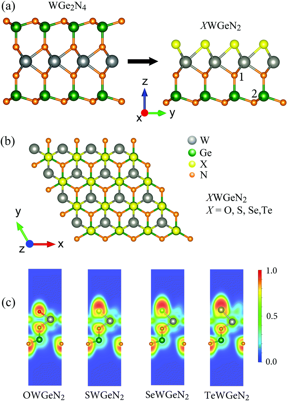 | ||
| Fig. 1 (a) Side views of monolayers WGe2N4 (left panel) and XWGeN2 (right panel); (b) top view of the atomic structure of XWGeN2 (X = O, S, Se, and Te) monolayers; and (c) electron localization function of XWGeN2. 1 and 2 in (a) indicate the N atoms in the middle and bottom N sublayers, respectively. The red and blue regions in (c) correspond to fully localized electrons and very low charge density, respectively. | ||
| a | d W–X | d W–N | d Ge–N1 | d Ge–N2 | Θ ∠X–W–X | Θ ∠X–N–Ge | Θ ∠N1–Ge–N2 | Θ ∠N2–Ge–N2 | Δh | E coh | |
|---|---|---|---|---|---|---|---|---|---|---|---|
| OWGeN2 | 2.96 | 2.09 | 2.11 | 1.87 | 1.82 | 90.27 | 126.03 | 110.67 | 108.25 | 4.96 | 8.30 |
| SWGeN2 | 3.06 | 2.39 | 2.13 | 1.87 | 1.86 | 79.40 | 124.17 | 108.44 | 110.48 | 5.28 | 7.83 |
| SeWGeN2 | 3.09 | 2.51 | 2.14 | 1.88 | 1.87 | 75.93 | 123.42 | 107.74 | 111.14 | 5.39 | 7.61 |
| TeWGeN2 | 3.16 | 2.70 | 2.15 | 1.89 | 1.90 | 76.61 | 122.13 | 106.46 | 112.31 | 5.56 | 7.28 |
We next estimate the cohesive energy Ecoh to examine the strength of chemical bonds in considered structures. The Ecoh value of XWGeN2 can be calculated according to the following formula:
 | (1) |
In Table 1, we list the calculated cohesive energies of XWGeN2. It is indicated that the four investigated monolayers of XWGeN2 are energetically favorable. The cohesive energy of XWGeN2 varies from 7.28 to 8.30 eV per atom. The OWGeN2 monolayer is the most energetically stable system with a cohesive energy of 8.30 eV per atom.
To get insights into the bonding nature of the investigated structures, the electron localization function (ELF) of XWGeN2 monolayers is evaluated and presented in Fig. 1(c). The blue (0.0), green (0.5), and red (1.0) domains refer to the very low density of charge, maximum delocalized electron, and maximum localized electron, respectively. It is found that the high electron localization is around the X and N atoms. For covalent bonds, the electrons which constitute the bonds are delocalized. This suggests that W–X or Ge–N bonds are covalent bonds. X and N atoms are positively charged while W and Ge are negatively charged. Our Bader charge analysis of atoms for XWGeN2, as listed in Table 2, indicates that the charge of X reduces from 1.03e to 0.01e as the X element varies from O to Te. This is related to the charge redistribution, which is dependent on the electronegativity difference between the X and W constituents.
| q X | q W | q Ge | q N1 | q N2 | |
|---|---|---|---|---|---|
| OWGeN2 | 1.03 | −1.94 | −1.61 | 1.37 | 1.15 |
| SWGeN2 | 0.30 | −1.08 | −1.63 | 1.27 | 1.14 |
| SeWGeN2 | 0.22 | −1.12 | −1.63 | 1.36 | 1.17 |
| TeWGeN2 | 0.01 | −0.90 | −1.63 | 1.35 | 1.17 |
Next, we analyze the phonon dispersions of XWGeN2 to examine their dynamical stability. In principle, the structure of materials is confirmed to be dynamically stable when its vibrational spectrum contains only positive frequencies. The restoring force will be gone if the phonon dispersions contain soft modes. The calculated phonon dispersions of XWGeN2 monolayers are shown in Fig. 2(a). The unit-cell of XWGeN2 contains five atoms. Therefore, there are 15 phonon modes (three acoustic and 12 optical modes) in its vibrational spectrum. At the Γ point, there are both doubly degenerate phonon modes (E modes) and four non-degenerate phonon modes (A1 modes) in the optical vibrational region. The A1 modes relate to the out-of-plane optical (ZO) branches and the E modes refer to a combination of the in-plane longitudinal (LO) and transverse (TO) optical vibrational branches at the Γ point. In all four vibrational spectra, we can see that no phonon gap is found between acoustic and optical phonon branches. It is observed that there is a range of frequencies where both phonon modes coexist in XWGeN2 monolayers. This may lead to robust optical–acoustic scattering, and then the materials will have low thermal conductivity. The structure of all four considered monolayers of XWGeN2 is confirmed to be dynamically stable because of the absence of the negative frequency in its phonon dispersions. Besides the evaluation of the phonon dispersions, we also perform the AIMD simulation to analyze the thermal stability of the considered structures. Fig. 2(b) shows the AIMD calculations for the total energy and temperature fluctuations at 300 K (room temperature) within 6 ps with each step of 1 fs. Our simulated results reveal that the total energy of the systems fluctuates only by about 0.5 eV and their temperature fluctuates at around 300 K during the whole simulated time. No chemical bonds break nor structural phase transitions were found. The atomic structure of the considered systems remains robust after heating within 6 ps, suggesting that all four structures of XWGeN2 are thermally stable at 300 K.
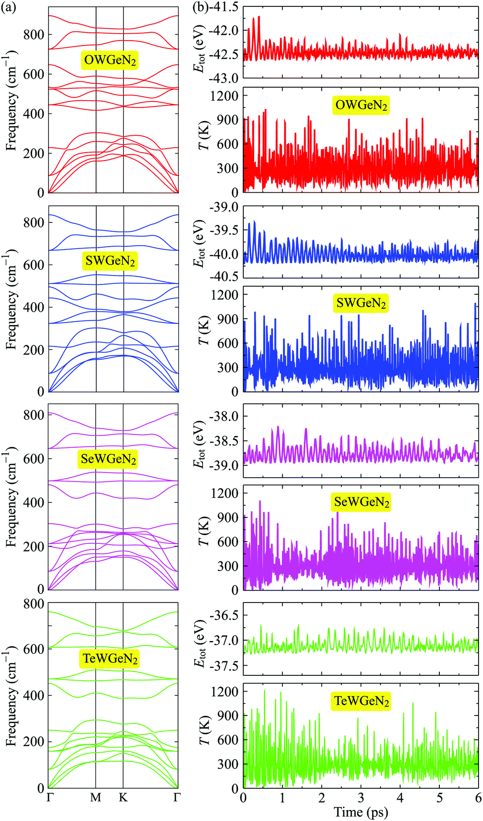 | ||
| Fig. 2 (a) Phonon dispersions and (b) AIMD simulations for the total energy Etot and temperature T fluctuations at room temperature of XWGeN2. | ||
Based on the analysis of stiffness coefficients, we also examine the mechanical stability of the considered structures. Generally, there are four independent stiffness coefficients Cij, including C11, C22, C12, and C66, and should be calculated. However, with the centered-hexagonal symmetry of XWGeN2 as shown in Fig. 1(a), only C11 and C12 should be calculated because C22 = C11 and C66 is calculated by C66 = (C11 − C12)/2. The elastic coefficients are obtained by parabolic fitting the strain-dependent elastic energy of the considered systems. In our calculations, we calculate the elastic energy of the monolayers at different values of the uniaxial strain εx (εy) in the range from −0.02 to 0.02 (each step being 0.005) along the two in-plane directions. This approach has previously been performed to calculate the stiffness coefficients of the other 2D nanosheets.44–46
In Table 3, we present the calculated results for the elastic stiffness coefficients of XWGeN2. It is calculated that both C11 and C12 decrease when the X constituent moves from O to Te. More importantly, XWGeN2 monolayers have the elastic stiffness coefficients satisfying Born–Huang's criteria for mechanical stability for the hexagonal structures: C11 > 0 and C112 > C122.42 Then we can conclude that XWGeN2 monolayers are mechanically stable.
| C 11 | C 12 | C 66 | Y 2D | ν | |
|---|---|---|---|---|---|
| OWGeN2 | 359.72 | 114.65 | 122.54 | 323.18 | 0.32 |
| SWGeN2 | 307.65 | 79.34 | 114.15 | 287.19 | 0.26 |
| SeWGeN2 | 295.32 | 68.26 | 113.53 | 279.54 | 0.23 |
| TeWGeN2 | 277.02 | 54.01 | 111.51 | 266.49 | 0.20 |
Young's modulus Y2D and Poisson's ratio ν, which can depend on the investigated direction (angle-dependent Y2D(α) and ν(α)), are calculated based on the elastic constants Cij by the following formulas:47,48
 | (2) |
 | (3) |
![[thin space (1/6-em)]](https://www.rsc.org/images/entities/char_2009.gif) α, B = cosα, and Π = (C11C22 − C122)/C66. α refers to the angle between the armchair and studied directions.
α, B = cosα, and Π = (C11C22 − C122)/C66. α refers to the angle between the armchair and studied directions.
Fig. 3 presents the polar diagrams of Y2D(α) and ν(α) for XWGeN2 structures. It is calculated that the polar diagrams of Y2D(α) and ν(α) are perfectly circles, implying both Y2D and ν do not depend on the angle α. This is due to the in-plane isotropic structures of XWGeN2. A similar angle-dependence of Y2D(α) and ν(α) is found in other isotropic 2D materials.14,49–51 Our calculated results indicate that Y2D of XWGeN2 is in the range from 266.49 N m−1 (TeWGeN2) to 323.18 N m−1 (OWGeN2), which is comparable with graphene (340 N m−1).52
 | ||
| Fig. 3 Angle-dependent Young's modulus Y2D(α) (a) and Poisson's ratio ν(α) (b) of XWGeN2. | ||
4 Electronic properties and the Rashba spin splitting effect
In this section, we show the calculated results for the electronic characteristics of XWGeN2 monolayers by using the DFT method. It is revealed that all four studied systems of the XWGeN2 structure are indirect semiconductors as shown in Fig. 4(a). It is shown that the calculated PBE and HSE06 band structures of XWGeN2 are similar profiles. However, the PBE method is known as a method that underestimates the bandgap value and the bandgap of semiconductors calculated by the HSE06 method is considered to have an acceptable accuracy. It is calculated that the HSE06 bandgap of XWGeN2 is from 1.54 to 2.44 eV, which is comparable to the bandgap of WGe2N4 (1.69 eV).28 The HSE06 bandgaps of SWGeN2 and SeWGeN2 are 2.44 and 2.43 eV, respectively. The OWGeN2 monolayer has the smallest bandgap of 1.54 eV (1.07 eV) at the HSE06 (PBE) level. For comparison, both the HSE06 and PBE bandgaps of XWGeN2 are presented in Table 4 and also shown in Fig. 4(b). As depicted in Fig. 4(a), it is found that the valence band maximum (VBM) and conduction band minimum (CBM) of OWGeN2 locate at the Γ and K points in the first Brillouin zone, respectively. Meanwhile, the VBM of the other three structures is shifted away from the Γ point and lies on the KΓ path (near the Γ point). The band structures of SWGeN2 and SeWGeN2 near the Fermi level are quite similar. For TeWGeN2, the CBM is on the KΓ path, i.e., it is different from the other structures. The electronic states of 2D structures are extremely sensitive to their atomic structure and structural perfection. Hence, the great difference in the atomic structure (lattice constant a and the W–X bond length dW–X) between OWGeN2 (TeWGeN2) and SWGeN2 or SeWGeN2 is one of the reasons for their band structure to be different. To evaluate the contribution of the orbitals of atoms in the compound to the band structure, we calculate the HSE06 weighted bands of XWGeN2 monolayers as presented in Fig. 5. As shown in Fig. 5, we can see that both the CBM and VBM of the studied monolayers are mainly contributed by the W-d orbitals. The p-orbital of the N atoms also makes a significant contribution to the VBM, in particular, in the cases of SWGeN2 and SeWGeN2. The X-p orbitals have a large contribution to the formation of the valence band far from the Fermi level, around −3 eV. Note that the contributions of atomic orbitals to the electronic bands calculated by the PBE and HSE06 functionals are the same.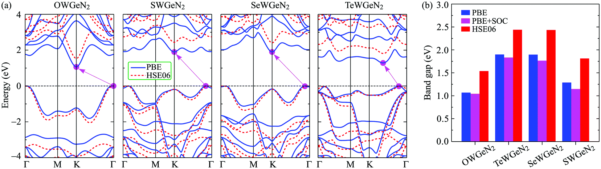 | ||
| Fig. 4 (a) PBE (solid curves) and HSE06 (dashed curves) electronic energy band diagrams and (b) band gaps of the XWGeN2 monolayers. | ||
| E PBEg | E HSE06g | E PBE+SOCg | λ v | E KR | E MR | k KR | k MR | α KR | α MR | |
|---|---|---|---|---|---|---|---|---|---|---|
| OWGeN2 | 1.07 | 1.54 | 1.04 | 0.44 | — | — | — | — | — | — |
| SWGeN2 | 1.90 | 2.44 | 1.83 | 0.42 | 15.9 | 15.6 | 0.087 | 0.086 | 366 | 359 |
| SeWGeN2 | 1.90 | 2.43 | 1.77 | 0.41 | 15.1 | 15.0 | 0.082 | 0.083 | 368 | 361 |
| TeWGeN2 | 1.29 | 1.81 | 1.15 | 0.33 | 37.4 | 36.6 | 0.127 | 0.121 | 589 | 605 |
 | ||
| Fig. 5 Weighted bands calculated by the HSE06 method of (a) OWGeN2, (b) SWGeN2, (c) SeWGeN2, and (d) TeWGeN2 monolayers. | ||
For heavy-constituent-based compounds, the effect of the SOC on the electronic characteristics is significant. The PBE + SOC band diagrams of XWGeN2 calculated in the M–K–Γ–M direction of the Brillouin zone are shown in Fig. 6. It is indicated that, when the SOC is included, the bandgaps of XWGeN2 significantly reduces, particularly in TeWGeN2. The PBE + SOC bandgap of TeWGeN2 is calculated to be 1.15 eV, which is much smaller than its PBE bandgap (1.29 eV) as presented in Table 4. When the SOC effect was introduced, the degeneracy of the spin at the CBM and VBM is removed and a large spin splitting energy λv at the K point in the valence band is found for all the four studied monolayers. The spin splitting energy λv is from 0.33 to 0.44 eV as presented in Table 4. Such a large spin-splitting energy was also previously found in the Janus WSeTe monolayer.53 More interestingly, the Rashba-type SOC splitting is found around the Γ point in the conduction band of three structures, including SWGeN2, SeWGeN2, and TeWGeN2. The magnified view of the Rashba splitting of these monolayers is also shown in Fig. 6. The Rashba effect strength can be described through the three key quantities, including the Rashba energy ER, Rashba momentum offset kR, and Rashba constant αR. ER and kR can be directly calculated from the band diagrams as depicted in Fig. 6 while the Rashba constant αR is calculated by the relationship αR = 2ER/kR.54–56 From Fig. 6, we can see that the Rashba parameters in different directions (i.e. the Γ–K and Γ–M directions) can be different. The Rashba energy ER is defined by the energy difference between the degenerate energy at the Γ point and the two peaks as shown in Fig. 6 (EKR for the peak in the Γ–M direction and EMR for the peak in the Γ–M direction).
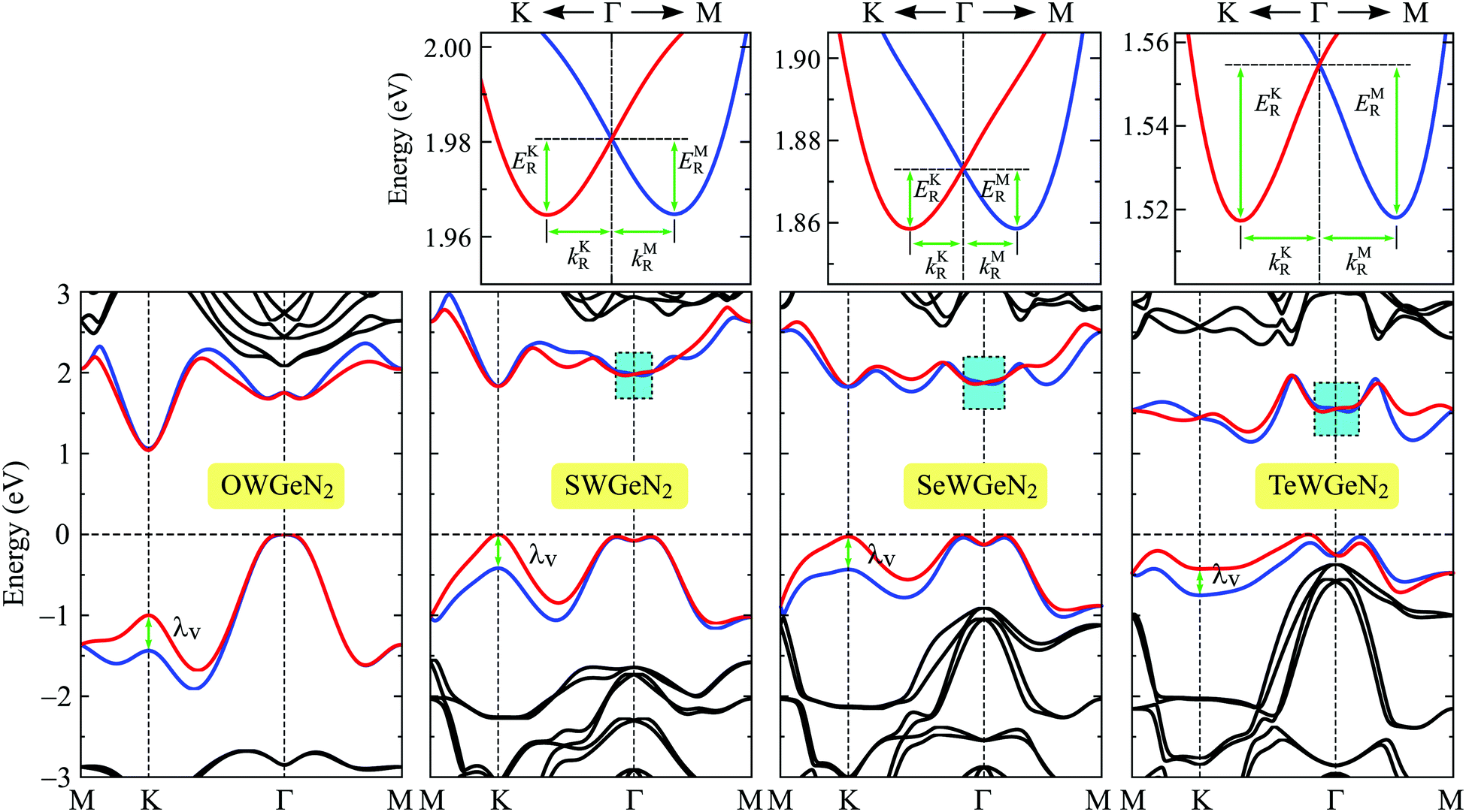 | ||
| Fig. 6 Band diagrams of XWGeN2 monolayers with spin–orbit coupling. The small figures at the top are the magnified view of the lowest conduction bands around the Γ point. | ||
We show the obtained results for the Rashba parameters in the Γ–M and Γ–K high-symmetry directions in Table 4. It is revealed that the Rashba parameters in the Γ–K direction (EKR, kKR, αKR) are very close to those in the Γ–M direction (EMR, kMR, αMR). The maximum value of the Rashba energy is found to be 37.4 meV for TeWGeN2 in the Γ–K direction. Previously, a giant Rashba energy of 52.0 meV was reported in WSeTe.53 The Rashba constants αKR (αMR) are found to be 369(366), 360(354), and 589(605) meV Å for SWGeN2, SeWGeN2, and TeWGeN2, respectively. The difference between αKR and αMR is quite small. Therefore, we roughly conclude that the Rashba parameters of XWGeN2 are directionally isotropic in the Brillouin zone. It is found that, as listed in Table 4, αR increases when the X constituent of the compound moves from S to Te. This is due to the increase in the SOC strength of the chalcogen constituent. However, there is no significant difference in the Rashba constant αR between the SWGeN2 and SWGeN2 monolayers. Similar trends in the Rashba constant have also been found previously in Janus transition metal dichalcogenides and the Rashba constant of WSeTe was reported to be up to 524 meV Å.55
Strain engineering is considered an effective way to control the electronic characteristics of 2D nanomaterials. Here, we examine the effect of a biaxial strain εb on the electronic characteristics of XWGeN2 by using the PBE approach. The biaxial strain can be defined as εb = (t − t0)/t0, where t0 and t are the lattice parameters of the unstrained and strained monolayers. In our calculations, the biaxial strain ranges from 0 to ±10%. Here, the “±” sign indicates the compressive/tensile strain. It is indicated that the indirect semiconductor behaviors of all four XWGeN2 monolayers are preserved in the presence of the biaxial strain with a strain range of −10 to +10% (not shown). No phase transitions are found in the strained XWGeN2. However, the bandgap of XWGeN2 dramatically changes when εb is applied. Fig. 7 presents the calculated results for the dependence of the PBE bandgaps of XWGeN2 on εb. It is shown that the tensile strain rapidly reduces the bandgap of XWGeN2 monolayers. The graphs showing the dependence of the bandgap on the biaxial strain for monolayers containing chalcogen atoms S, Se, and Te (i.e. SWGeN2, SeWGeN2, TeWGeN2) are similar. This characteristic is consistent with similar 2D compounds based on chalcogenides.57 The bandgap of these monolayers increases slightly and then decreases under the compressive strain. Meanwhile, the bandgap of OWGeN2 increases under the compressive strain.
 | ||
| Fig. 7 Dependence of the PBE bandgaps of XWGeN2 monolayers on the biaxial strain εb. | ||
5 Transport properties
In the last part, we show our predictions for the transport properties of the four XWGeN2 structures. We focus on the carrier mobility and related transport parameters of the considered systems. The mobilities of carriers can be evaluated by using the deformation potential approximation.43 For 2D nanomaterials, the mobility of the carrier μ2D is calculated as follows:58 | (4) |
 is the average effective mass. In our calculations, the temperature T is selected to be 300 K (room temperature).
The carrier effective mass, according to eqn (4), is one of the most important parameters, which strongly influences the carrier mobility. The carriers will respond quickly to the external field if they have low effective mass and vice versa. We can obtain the carrier mass m* by fitting the parabolic function to the band edge positions (the VBM for holes and the CBM for electrons) through the formula as follows:
 | (5) |
The effective masses of carriers are dependent on the band structure around the CBB/VBM. We can see that, as shown in eqn (5), the carrier effective mass m* is inversely proportional to the second derivative ∂2E(k)/∂k2. Then, m* will be high if the band structure around the CBB/VBM is flat (large radius of curvature). The calculated results for the effective mass of electrons and holes along the transport directions mx* and my* are tabled in Table 4. It is shown that the effective masses of carriers are directionally isotropic (mx* = my*). However, a large difference in the effective mass between electrons me* and holes mh* is found, particularly in the case of the OWGeN2 monolayer. This is due to the difference in the radius of the curvature around the CMB (for electrons) and VBM (for holes) as shown in Fig. 4. For example, the band diagram around the VBM for OWGeN2 has a larger radius of curvature (flatter) than that around the CBM. Consequently, the mh* of OWGeN2 is higher than its me*. It is calculated that me* of XWGeN2 is from 0.39m0 to 0.80m0, where m0 is the free electron mass. The me* of OWGeN2, SWGeN2, and SeWGeN2 monolayers are smaller than mh*. This suggests that the electrons in these structures will respond to the external fields more quickly than holes. Meanwhile, in the case of TeWGeN2, our calculated results indicate that me* < mh*. This greatly affects the electron mobility in comparison to the hole mobility. However, as presented in eqn (4), the carrier mobility of 2D nanostructures depends also on C2D and Ed.
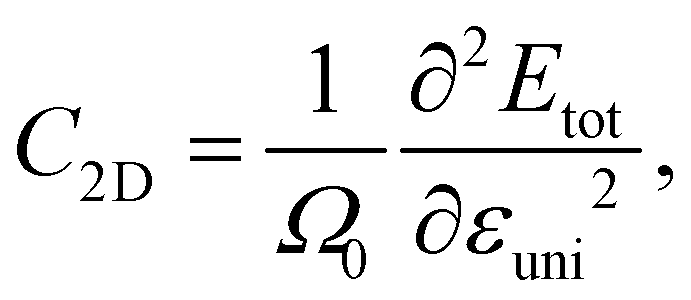
The elastic modulus C2D of 2D structures can be calculated by the following expression:
 | (6) |
 | (7) |
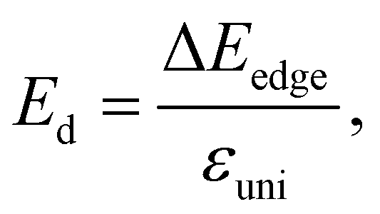
In our calculations, the strain-dependence of energies was investigated in the applied strain range from −1 to 1% (with each step being 0.5%) along the transport directions x and y. We fit the strain-dependence of energies to obtain C2D and Ed as introduced in previous studies.58,59 In Fig. 8, we present the energy changing and CBM/VBM positions as a function of εuni. The calculated results for both C2D and Ed of XWGeN2 are listed in Table 4. The C2D of XWGeN2 is high directionally isotropic. However, a directional anisotropy of Ed is found in TeWGeN2. The ratio of Ed for electrons along transport directions in XWGeN2 is calculated to be |Exd/Eyd| = 1.81. Recently, the anisotropy of Ed in isotropic 2D structures, such as Al2Se3 or Ga2Te3 monolayers, was reported.60 A large ratio of |Exd/Eyd| = 3.87 was observed in Ga2Te3.60 Such a directional anisotropy will lead to the anisotropy in the carrier mobility of the considered structures (Table 5).
 | ||
| Fig. 8 The uniaxial strain εx/yuni dependent energy shifting (a) CBM/VBM positions (b) of XWGeN2 along the two transport directions x and y. The fitting curves are presented by the solid lines. | ||
| m x * | m y * | C x 2D | C y 2D | E x d | E y d | μ x | μ y | ||
|---|---|---|---|---|---|---|---|---|---|
| OWGeN2 | Electron | 0.39 | 0.39 | 208.99 | 209.05 | −9.97 | −10.01 | 311.70 | 309.04 |
| Hole | 3.10 | 3.10 | 208.99 | 209.05 | −2.96 | −2.96 | 52.74 | 52.76 | |
| SWGeN2 | Electron | 0.41 | 0.41 | 181.38 | 181.34 | −10.67 | −10.77 | 204.84 | 201.01 |
| Hole | 1.45 | 1.45 | 181.38 | 181.34 | −3.03 | −3.16 | 151.55 | 139.67 | |
| SeWGeN2 | Electron | 0.61 | 0.61 | 175.03 | 175.35 | −8.51 | −7.52 | 34.43 | 44.20 |
| Hole | 0.89 | 0.89 | 175.03 | 175.35 | −3.63 | −3.60 | 241.69 | 246.45 | |
| TeWGeN2 | Electron | 0.80 | 0.80 | 165.34 | 165.47 | −7.25 | −4.00 | 58.55 | 192.89 |
| Hole | 0.58 | 0.58 | 165.34 | 165.47 | −5.52 | −4.74 | 220.92 | 300.29 | |
The obtained results for the carrier mobility μ of XWGeN2 are presented in Table 4. It is calculated that the electron mobility of XWGeN2 is high, up to 311.70 cm2 V−1 s−1 for OWGeN2. The carrier mobilities of OWGeN2, SWGeN2, and SeWGeN2 are quite directionally isotropic. The difference in the carrier mobility between the different directions μx,y in these structures is small. However, there is a large difference between μx and μy for electrons in the case of TeWGeN2. The electron mobility of TeWGeN2 is calculated to be μx = 58.55 cm2 V−1 s−1 and μy = 192.89 cm2 V−1 s−1. This is due to the directional anisotropy of the deformation potential constant Ed in TeWGeN2 as above-mentioned. It is also found that, in SeWGeN2 and TeWGeN2 monolayers, the mobilities of holes are higher than those of electrons. This is different from the other two structures, i.e., OWGeN2 and SWGeN2, which have an electron mobility much larger than the hole mobility. With a high electron mobility, the XWGeN2 monolayers, such as OWGeN2 and SWGeN2, are suitable for applications in high-speed electronic nanodevices.
6 Conclusions
In conclusion, we have suggested new stable monolayers of the Janus XWGeN2 which have a quintuple-layer atomic structure. Our DFT calculations indicated that these monolayers are indirect semiconductors and their bandgap can be controlled by applied strains. The Rashba-type SOC with a large Rashba constant is found around the Γ point of SWGeN2, SeWGeN2, and TeWGeN2. The obtained calculations indicate that the Rashba parameters of these three monolayers are not too sensitive to the investigated directions in the first Brillouin zone. The existence of the giant Rashba SOC effect together with the large bandgap makes these materials promising for applications in highly efficient spintronic and optoelectronic devices. OWGeN2 has the highest electron mobility of 311.70 and 309.04 cm2 V−1 s−1 along the transport directions x and y, respectively. Our findings not only provide important physical characteristics of XWGeN2 systems but also guide further investigations on quintuple-layer atomic Janus materials formed from the symmetric structures of the MA2Z4 family.Conflicts of interest
There are no conflicts of interest to declare.Acknowledgements
Tuan V. Vu would like to thank the Van Lang University for funding this work.References
- K. S. Novoselov, A. K. Geim, S. V. Morozov, D. Jiang, Y. Zhang, S. V. Dubonos, I. V. Grigorieva and A. A. Firsov, Science, 2004, 306, 666 CrossRef CAS PubMed.
- K. S. Novoselov, V. I. Fal'ko, L. Colombo, P. R. Gellert, M. G. Schwab and K. Kim, Nature, 2012, 490, 192–200 CrossRef CAS PubMed.
- N. A. Poklonski, S. A. Vyrko, A. I. Siahlo, O. N. Poklonskaya, S. V. Ratkevich, N. N. Hieu and A. A. Kocherzhenko, Mater. Res. Express, 2019, 6, 042002 CrossRef.
- S. Cahangirov, M. Topsakal, E. Aktürk, H. Sahin and S. Ciraci, Phys. Rev. Lett., 2009, 102, 236804 CrossRef CAS PubMed.
- M. E. Dávila, L. Xian, S. Cahangirov, A. Rubio and G. Le Lay, New J. Phys., 2014, 16, 095002 CrossRef.
- L. Song, L. Ci, H. Lu, P. B. Sorokin, C. Jin, J. Ni, A. G. Kvashnin, D. G. Kvashnin, J. Lou, B. I. Yakobson and P. M. Ajayan, Nano Lett., 2010, 10, 3209–3215 CrossRef CAS PubMed.
- A. Harvey, C. Backes, Z. Gholamvand, D. Hanlon, D. McAteer, H. C. Nerl, E. McGuire, A. Seral-Ascaso, Q. M. Ramasse, N. McEvoy, S. Winters, N. C. Berner, D. McCloskey, J. F. Donegan, G. S. Duesberg, V. Nicolosi and J. N. Coleman, Chem. Mater., 2015, 27, 3483 CrossRef CAS.
- F. Liu, H. Shimotani, H. Shang, T. Kanagasekaran, V. Zólyomi, N. Drummond, V. I. Falko and K. Tanigaki, ACS Nano, 2014, 8, 752–760 CrossRef CAS PubMed.
- D. Kong, H. Wang, J. J. Cha, M. Pasta, K. J. Koski, J. Yao and Y. Cui, Nano Lett., 2013, 13, 1341–1347 CrossRef CAS PubMed.
- L. Yi-Hsien, Z. Xin-Quan, Z. Wenjing, C. Mu-Tung, L. Cheng-Te, C. Kai-Di, Y. Ya-Chu, W. J. Tse-Wei, C. Chia-Seng, L. Lain-Jong and L. Tsung-Wu, Adv. Mater., 2012, 24, 2320–2325 CrossRef PubMed.
- A.-Y. Lu, H. Zhu, J. Xiao, C.-P. Chuu, Y. Han, M.-H. Chiu, C.-C. Cheng, C.-W. Yang, K.-H. Wei, Y. Yang, Y. Wang, D. Sokaras, D. Nordlund, P. Yang, D. A. Muller, M.-Y. Chou, X. Zhang and L.-J. Li, Nat. Nanotechnol., 2017, 12, 744 CrossRef CAS PubMed.
- J. Zhang, S. Jia, I. Kholmanov, L. Dong, D. Er, W. Chen, H. Guo, Z. Jin, V. B. Shenoy, L. Shi and J. Lou, ACS Nano, 2017, 11, 8192–8198 CrossRef CAS PubMed.
- W. Zhou, J. Chen, Z. Yang, J. Liu and F. Ouyang, Phys. Rev. B: Condens. Matter Mater. Phys., 2019, 99, 075160 CrossRef.
- T. V. Vu, V. T. T. Vi, H. V. Phuc, A. I. Kartamyshev and N. N. Hieu, Phys. Rev. B: Condens. Matter Mater. Phys., 2021, 104, 115410 CrossRef CAS.
- T. V. Vu, C. V. Nguyen, H. V. Phuc, A. A. Lavrentyev, O. Y. Khyzhun, N. V. Hieu, M. M. Obeid, D. P. Rai, H. D. Tong and N. N. Hieu, Phys. Rev. B: Condens. Matter Mater. Phys., 2021, 103, 085422 CrossRef CAS.
- T. V. Vu, V. T. T. Vi, C. V. Nguyen, H. V. Phuc and N. N. Hieu, J. Phys. D: Appl. Phys., 2020, 53, 455302 CrossRef CAS.
- H. T. T. Nguyen, V. V. Tuan, C. V. Nguyen, H. V. Phuc, H. D. Tong, S.-T. Nguyen and N. N. Hieu, Phys. Chem. Chem. Phys., 2020, 22, 11637–11643 RSC.
- S. Sinha, T. Zhu, A. France-Lanord, Y. Sheng, J. C. Grossman, K. Porfyrakis and J. H. Warner, Nat. Commun., 2020, 11, 823 CrossRef CAS PubMed.
- C. V. Nguyen, M. Idrees, H. V. Phuc, N. N. Hieu, N. T. T. Binh, B. Amin and T. V. Vu, Phys. Rev. B: Condens. Matter Mater. Phys., 2020, 101, 235419 CrossRef CAS.
- H. T. T. Nguyen, M. M. Obeid, A. Bafekry, M. Idrees, T. V. Vu, H. V. Phuc, N. N. Hieu, L. T. Hoa, B. Amin and C. V. Nguyen, Phys. Rev. B: Condens. Matter Mater. Phys., 2020, 102, 075414 CrossRef CAS.
- T. V. Vu, N. V. Hieu, H. V. Phuc, N. N. Hieu, H. Bui, M. Idrees, B. Amin and C. V. Nguyen, Appl. Surf. Sci., 2020, 507, 145036 CrossRef CAS.
- W. Jin, W. Sun, X. Kuang, C. Lu and L. Kou, J. Phys. Chem. Lett., 2020, 11, 9643–9648 CrossRef CAS PubMed.
- Y. Wang, S.-S. Wang, Y. Lu, J. Jiang and S. A. Yang, Nano Lett., 2016, 16, 4576–4582 CrossRef CAS PubMed.
- S.-H. Zhang and B.-G. Liu, Nanotechnology, 2018, 29, 325401 CrossRef PubMed.
- X. P. Du, Y. X. Wang and V. Lo, Phys. Lett. A, 2010, 374, 2569–2574 CrossRef CAS.
- Q. Li, L. He, C. Sun and X. Zhang, J. Phys. Chem. C, 2017, 121, 27563–27568 CrossRef CAS.
- X. Yang, X. Xu, X. Hou, P. Zhang, J. Mi, B. Xiao, J. Huang and C. Stampfl, Catal. Commun., 2021, 149, 106212 CrossRef CAS.
- Y.-L. Hong, Z. Liu, L. Wang, T. Zhou, W. Ma, C. Xu, S. Feng, L. Chen, M.-L. Chen, D.-M. Sun, X.-Q. Chen, H.-M. Cheng and W. Ren, Science, 2020, 369, 670–674 CrossRef CAS PubMed.
- C. Q. Nguyen, Y. S. Ang, S.-T. Nguyen, N. V. Hoang, N. M. Hung and C. V. Nguyen, Phys. Rev. B: Condens. Matter Mater. Phys., 2022, 105, 045303 CrossRef CAS.
- C. V. Nguyen, C. Q. Nguyen, S.-T. Nguyen, Y. S. Ang and N. V. Hieu, J. Phys. Chem. Lett., 2022, 13, 2576–2582 CrossRef CAS PubMed.
- A. Ray, S. Tyagi, N. Singh and U. Schwingenschlögl, ACS Omega, 2021, 6, 30371–30375 CrossRef CAS PubMed.
- L. Wang, Y. Shi, M. Liu, A. Zhang, Y.-L. Hong, R. Li, Q. Gao, M. Chen, W. Ren, H.-M. Cheng, Y. Li and X.-Q. Chen, Nat. Commun., 2021, 12, 2361 CrossRef CAS PubMed.
- S. Li, W. Wu, X. Feng, S. Guan, W. Feng, Y. Yao and S. A. Yang, Phys. Rev. B: Condens. Matter Mater. Phys., 2020, 102, 235435 CrossRef CAS.
- C. Shen, L. Wang, D. Wei, Y. Zhang, G. Qin, X.-Q. Chen and H. Zhang, Phys. Chem. Chem. Phys., 2022, 24, 3086–3093 RSC.
- P. Giannozzi, S. Baroni, N. Bonini, M. Calandra, R. Car, C. Cavazzoni, D. Ceresoli, G. L. Chiarotti, M. Cococcioni, I. Dabo, A. D. Corso, S. de Gironcoli, S. Fabris, G. Fratesi, R. Gebauer, U. Gerstmann, C. Gougoussis, A. Kokalj, M. Lazzeri, L. Martin-Samos, N. Marzari, F. Mauri, R. Mazzarello, S. Paolini, A. Pasquarello, L. Paulatto, C. Sbraccia, S. Scandolo, G. Sclauzero, A. P. Seitsonen, A. Smogunov, P. Umari and R. M. Wentzcovitch, J. Phys.: Condens. Matter, 2009, 21, 395502 CrossRef PubMed.
- S. Grimme, J. Comput. Chem., 2006, 27, 1787 CrossRef CAS PubMed.
- A. H. MacDonald, W. E. Picket and D. D. Koelling, J. Phys. C: Solid State Phys., 1980, 13, 2675 CrossRef CAS.
- J. Heyd, G. E. Scuseria and M. Ernzerhof, J. Chem. Phys., 2003, 118, 8207 CrossRef CAS.
- L. Bengtsson, Phys. Rev. B: Condens. Matter Mater. Phys., 1999, 59, 12301 CrossRef CAS.
- A. Togo, F. Oba and I. Tanaka, Phys. Rev. B: Condens. Matter Mater. Phys., 2008, 78, 134106 CrossRef.
- M. Born and K. Huang, Am. J. Phys., 1955, 23, 474 CrossRef.
- R. C. Andrew, R. E. Mapasha, A. M. Ukpong and N. Chetty, Phys. Rev. B: Condens. Matter Mater. Phys., 2012, 85, 125428 CrossRef.
- J. Bardeen and W. Shockley, Phys. Rev., 1950, 80, 72 CrossRef CAS.
- K.-A. N. Duerloo, M. T. Ong and E. J. Reed, J. Phys. Chem. Lett., 2012, 3, 2871–2876 CrossRef CAS.
- W.-Z. Xiao, G. Xiao and L.-L. Wang, J. Chem. Phys., 2016, 145, 174702 CrossRef PubMed.
- Y. Guo, S. Zhou, Y. Bai and J. Zhao, Appl. Phys. Lett., 2017, 110, 163102 CrossRef.
- N. T. Hung, A. R. T. Nugraha and R. Saito, J. Phys. D: Appl. Phys., 2018, 51, 075306 CrossRef.
- P. Xiang, S. Sharma, Z. M. Wang, J. Wu and U. Schwingenschlögl, ACS Appl. Mater. Interfaces, 2020, 12, 30731 CrossRef CAS PubMed.
- S.-D. Guo, X.-S. Guo, R.-Y. Han and Y. Deng, Phys. Chem. Chem. Phys., 2019, 21, 24620 RSC.
- T.-N. Do, N. N. Hieu, N. A. Poklonski, N. T. T. Binh, C. Q. Nguyen and N. D. Hien, RSC Adv., 2021, 11, 28381–28387 RSC.
- E. Cadelano, P. L. Palla, S. Giordano and L. Colombo, Phys. Rev. B: Condens. Matter Mater. Phys., 2010, 82, 235414 CrossRef.
- D. G. Papageorgiou, I. A. Kinloch and R. J. Young, Prog. Mater. Sci., 2017, 90, 75–127 CrossRef CAS.
- Q.-F. Yao, J. Cai, W.-Y. Tong, S.-J. Gong, J.-Q. Wang, X. Wan, C.-G. Duan and J. H. Chu, Phys. Rev. B: Condens. Matter Mater. Phys., 2017, 95, 165401 CrossRef.
- S. Singh and A. H. Romero, Phys. Rev. B: Condens. Matter Mater. Phys., 2017, 95, 165444 CrossRef.
- T. Hu, F. Jia, G. Zhao, J. Wu, A. Stroppa and W. Ren, Phys. Rev. B: Condens. Matter Mater. Phys., 2018, 97, 235404 CrossRef CAS.
- Y. Zhai, S. Baniya, C. Zhang, J. Li, P. Haney, C.-X. Sheng, E. Ehrenfreund and Z. V. Vardeny, Sci. Adv., 2017, 3, e170070 Search PubMed.
- N. N. Hieu, H. V. Phuc, A. I. Kartamyshev and T. V. Vu, Phys. Rev. B: Condens. Matter Mater. Phys., 2022, 105, 075402 CrossRef CAS.
- W. Wan, S. Zhao, Y. Ge and Y. Liu, J. Phys.: Condens. Matter, 2019, 31, 435501 CrossRef CAS PubMed.
- S.-D. Guo, W.-Q. Mu, Y.-T. Zhu, R.-Y. Han and W.-C. Ren, J. Mater. Chem. C, 2021, 9, 2464–2473 RSC.
- C.-F. Fu, J. Sun, Q. Luo, X. Li, W. Hu and J. Yang, Nano Lett., 2018, 18, 6312–6317 CrossRef CAS PubMed.
| This journal is © the Owner Societies 2022 |