
Electrically-driven robust tuning of lattice thermal conductivity†
E
Zhou‡
 a,
Donghai
Wei‡
a,
Jing
Wu
a,
Guangzhao
Qin
*a and
Ming
Hu
*b
a,
Donghai
Wei‡
a,
Jing
Wu
a,
Guangzhao
Qin
*a and
Ming
Hu
*b
aState Key Laboratory of Advanced Design and Manufacturing for Vehicle Body, College of Mechanical and Vehicle Engineering, Hunan University, Changsha, 410082, P. R. China. E-mail: gzqin@hnu.edu.cn
bDepartment of Mechanical Engineering, University of South Carolina, Columbia, SC 29208, USA. E-mail: hu@sc.edu
First published on 29th June 2022
Abstract
The two-dimensional (2D) materials, represented by graphene, stand out in the electrical industry applications of the future and have been widely studied. As commonly existing in electronic devices, the electric field has been extensively utilized to modulate the performance. However, how the electric field regulates thermal transport is rarely studied. Herein, we investigate the modulation of thermal transport properties by applying an external electric field ranging from 0 to 0.4 V Å−1, with bilayer graphene, monolayer silicene, and germanene as study cases. The monotonically decreasing trend of thermal conductivity in all three materials is revealed. A significant effect on the scattering rate is found to be responsible for the decreased thermal conductivity driven by the electric field. Further evidence shows that the reconstruction of internal electric field and generation of induced charges lead to increased scattering rate from strong phonon anharmonicity. Thus, the ultralow thermal conductivity emerges with the application of external electric fields. Applying an external electric field to regulate thermal conductivity illustrates a constructive idea for highly efficient thermal management.
1. Introduction
In 2004, Geim et al. found that graphene could stably exist in the environment by ‘peeling’ method to exfoliation.1 Inspired by graphene, more two-dimensional (2D) materials, such as the group IV analogues,2–5 group V analogues,6,7 MXenes,8–10 transition metal dichalcogenides,11 and BiXene12 have emerged and been widely explored for their outstanding physical and chemical properties. The applications of 2D materials have promoted the development of thermoelectricity, photoelectricity, nanoelectronics, etc. However, the currently reported materials, albeit with excellent properties, are still powerless for practical application when facing the ever-increasing requirements in extreme conditions. To purposefully obtain better properties, many effective control strategies, such as strain engineering, patterned cuts, doping, defects, dislocations, rotating between layers, external magnetic field, and external electric field have been adopted.6,13–29 These superior strategies greatly expand the applications of the pristine materials by leading to extraordinary properties.Typically, materials with high thermal conductivity (κ) are mainly applied for heat dissipation, and they have extensive applications in many fields, particularly in large CPU clusters, space vehicles, and nuclear reactors.30 Unfortunately, the semimetal electronic nature of graphene prohibits its potential applications despite its ultrahigh thermal conductivity. From 1994, silicene, the counterpart of silicon to graphene, has been well proven to have a promising future in the field of electronics from a theoretical perspective. However, the air stability of silicene limits its practical application.31–33 In 2015, Li et al. achieved the encapsulation of silicene by the silicene-encapsulated delamination with native electrodes (SEDNE) method, which can also be applied in fabricating germanene.34 Besides, they reported a new type of silicene-based field effect transistor (FET) and verified its better electronic characteristics compared with graphene, which are consistent with theoretical predictions, such as a small bandgap and high carrier mobility. Thus, the 2D materials represented by silicene have generated a research upsurge in the field of nanoelectronics. As a major factor affecting the performance and life of electronic devices, the heat dissipation ability quantified by thermal conductivity is a key parameter for device design. However, despite the common existence of electric fields in electronics, the effect of the electric field on thermal transport has been rarely studied. Note that there is no influence of external electric field on the thermal conductivity of monolayer graphene, which is restricted by the symmetry.35 As for bilayer silicene and germanene, there are covalent bonds between layers.36,37 Considering that graphene, silicene, and germanene are two-dimensional materials in group IV with similar Dirac cones in electronic structure, it is of great significance to study the regulating effect of an external electric field on the heat transfer performance of the systems.
In this paper, an external electric field was employed to explore its influence on the thermal conductivity of the AB stacked bilayer graphene,38 monolayer silicene, and germanene.39 We demonstrate that thermal conductivity is negatively correlated with the applied electric field, decreasing about 1–3 orders of magnitude for the bilayer graphene, monolayer silicene and germanene. A series of fundamental insights from the scattering rate, dielectric constant, and microscopic view of the electronic structure was conducted, as discussed in the following parts, to reveal the inherent mechanism for the electrically driven robust tuning of lattice thermal conductivity. The significantly modulated thermal conductivity of bilayer graphene, silicene, and germanene not only verifies the possibility of using an electric field to tune thermal transportation but also provides a remarkable scheme for applications in other fields.
2. Computational methodology
First-principles calculations were conducted based on density functional theory (DFT) using the Perdew–Burke–Ernzerhof generalized gradient approximation (PBE-GGA)40 as an exchange-correlation functional in the Vienna ab initio simulation package (VASP),41 followed by solving the phonon Boltzmann transport equation (BTE). The kinetic energy cutoff, energy convergence threshold, and the Hellmann–Feynman force were taken as 1000 eV, 10−8 eV, and 10−8 eV Å−1, respectively. The maximum strength of the electric field applied in the out-of-plane direction is up to 0.4 V Å−1 to make sure all the structures hold stability, where there is no imaginary frequency in the phonon spectrum. The dipole correction was taken into account throughout the calculation process, and van der Waals (vdW) forces were applied for the bilayer graphene in AB stacking. A 15 × 15 × 1 Monkhorst–Pack42k-point grid was used to sample the first Brillouin zone, and a vacuum layer of 20 Å was employed along the out-of-plane direction to avoid layer-to-layer interaction caused by periodic boundary conditions.Based on the density functional perturbation theory (DFPT), the Born effective charge and dielectric constant (ε) were calculated. Using the real-space finite displacement difference method applied in Phonopy43 and thirdorder.py,44 harmonic and nonharmonic force constants were obtained, respectively. The scattering matrix could be constructed based on the third-order force constant, and then we could calculate the phonon scattering rate and obtain the phonon relaxation time. Based on the convergence test, the 5th nearest neighbor was chosen as the cutoff radius for achieving the converged thermal conductivity. The κ was obtained by using the ShengBTE software package,45 solving the phonon BTE iteratively.
3. Results
Different from the planar honeycomb structure of graphene, both silicene and germanene have nonplanar bucking structure, as shown in the inset of Fig. 1. The thickness considering the vdW distance of germanene (4.889 Å)46 is greater than that of silicene (4.650 Å),47 which may be due to its larger relative atomic mass and radius. The lattice constants of the three materials increase exponentially with increasing electric field strength in the z direction (perpendicular to the plane). Despite the exponential increase of lattice constant, the variation of the absolute value is tiny (<0.03%). Moreover, the structural characteristics of the three materials were slightly affected, and the structure kept buckling for silicene and germanene. In addition, it is worth mentioning that the flatter the structure, the less the effect of the electric field on the lattice constant. On the contrary, the larger the bucking distance, the more obviously the lattice constant changes with the applied electric field.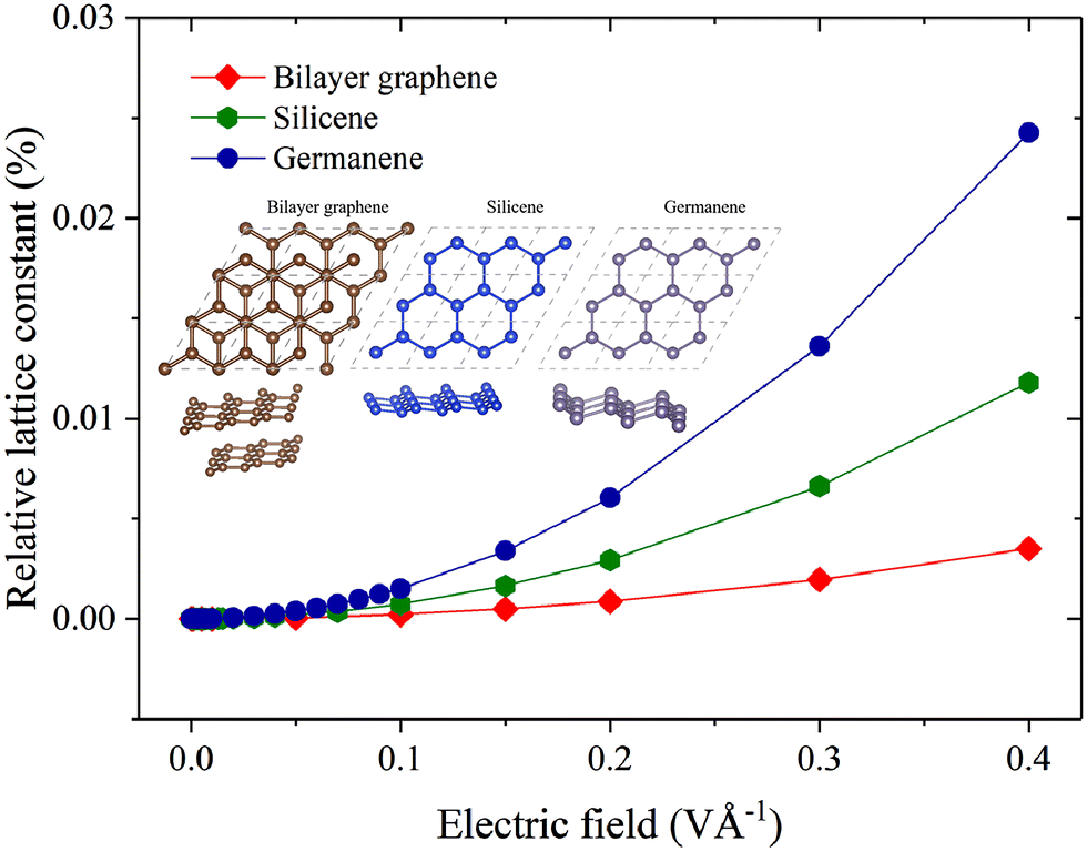 | ||
Fig. 1 Variation of lattice constant of AB stacking bilayer graphene, silicene, and germanene with respect to the strength of the external electric field (Ez) along the out-of-plane direction, where the relative lattice constant is calculated as 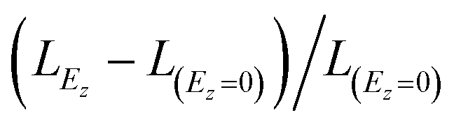 (Inset: The top and side views of structures of the optimized AB-stacked bilayer graphene, monolayer silicene, and germanene). (Inset: The top and side views of structures of the optimized AB-stacked bilayer graphene, monolayer silicene, and germanene). | ||
To examine the effect of the electric field on the thermal transport properties of materials, we calculated the κ of bilayer graphene, monolayer silicene, and germanene with the applied electric field. Despite the relevant electronic properties being of great importance to the materials, in this study, we would like to focus on the lattice thermal conductivity and phonon thermal transport properties under external electric field, considering that the thermal transport in semiconductors is governed by phonon transport. Besides, the charge density can be redistributed with the applied electric field. Thus, the interatomic interactions and phonons are renormalized with the possible electron-phonon naturally involved based on state-of-art first-principles calculations. The variation of κ as a function of the strength of the electric field is presented in Fig. 2. Generally, the κ values of monolayer silicene and germanene are 19.21 and 15.50 W m−1 K−1, respectively, much lower than that of bilayer graphene (1021.86 W m−1 K−1) obtained with no external electric field, which are in good agreement with previous reports.3,48,49 With the increasing external electric field, the κ of the three materials shows a similar decreasing trend. Surprisingly, when Ez = 0.4 V Å−1, the κ of germanene greatly decreases to 0.034 W m−1 K−1, which is nearly three orders of magnitude lower than that of the pristine state and is close to that of air. With the promising ultralow κ, we expect the future experimental verification and confirmation of the ultralow thermal conductivity of germanene under external electric field.
 | ||
| Fig. 2 Lattice thermal conductivity of bilayer graphene, monolayer silicene and germanene with the applied electric field ranging from 0 to 0.4 V Å−1. The original and reoptimized structures correspond to the calculations based on the pristine structure without electric field applied and the fully optimized structure with electric field applied, respectively. | ||
The κ dependence of the phonon mean free path (MFP) of bilayer graphene was further studied, as shown in ESI† Fig. S3. The representative mean free path corresponding to 50% κ decreases with the increased external electric field. It has been indicated by recent studies that phonons have wave-particle duality.50,51 The particle properties of phonons were calculated by ShengBTE based on the phonon gas model. With the electric field applied, the κ contribution due to the wave behavior of phonons would also be an essential factor leading to the ultralow thermal conductivity.
In addition, considering the tiny effect of electric field on the geometry parameters, we further calculated κ based on the original structure to make a comparison, where the pristine structure without electric field applied was used for all the calculations with the electric field applied. Noticeably, there is almost no difference in the κ of the three materials whether or not the structure is optimized. The results indicate that geometry variation is not responsible for the great effect of the electric field on κ, and there must be other factors dominating the variation of κ.
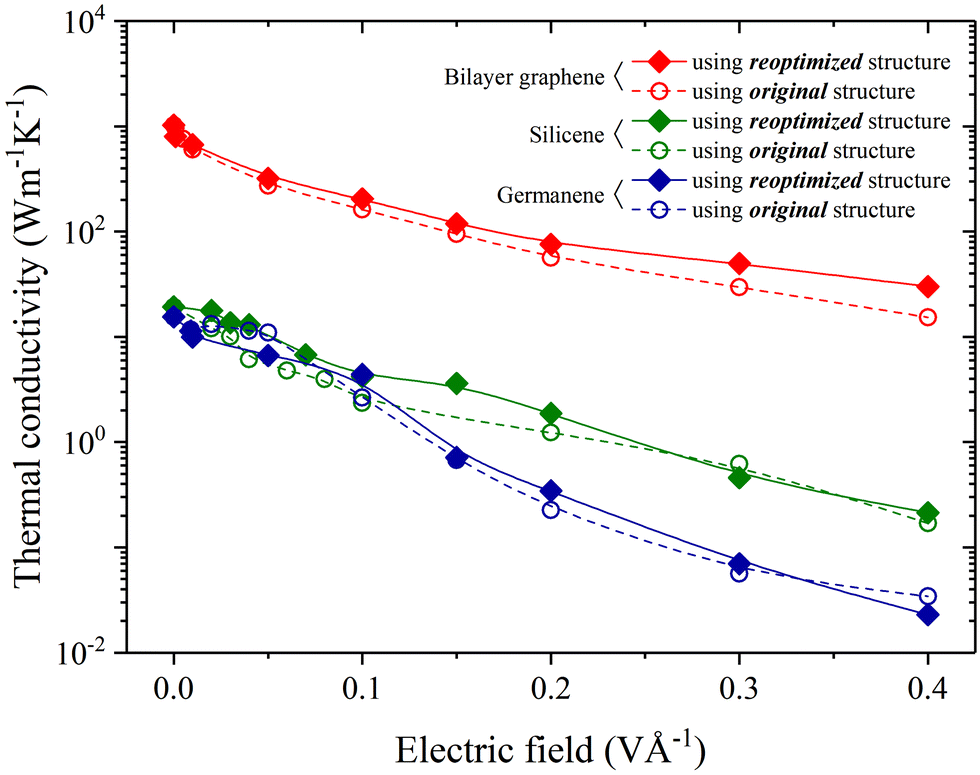
It has been reported that the external electric field has a very slight effect on the phonon spectrum,52 which is also confirmed in this study for bilayer graphene, monolayer silicene and germanene. Consequently, group velocities and the specific heat capacity of bilayer graphene, monolayer silicene, germanene are almost unaffected by the electric field. Thus, the only factor left is relaxation time, which must be the primary reason for the decreasing and unique response trends of κ26,53 as revealed in Fig. 2. To figure out the issue, we accessed the variation of the scattering rate with respect to the electric field strength, as schematized in Fig. 3. When the strength of Ez keeps increasing, the scattering rate of the three materials increases significantly. Additionally, the scattering intensity of bilayer graphene is much lower than those of monolayer silicene and germanene under the same external electric field, such as Ez = 0.3 V Å−1, which explains why the κ of bilayer graphene is much higher than that of silicene and germanene.
 | ||
| Fig. 3 Phonon scattering rate under the representative electric field (red for 0 V Å−1, green for 0.1 V Å−1, blue for 0.3 V Å−1) of the (a) bilayer graphene, (b) monolayer silicene, and (c) germanene. | ||
Besides, germanene has the highest scattering rate, especially in the region of large electric field, which shows a variation trend consistent with the κ discussed above. It can be clearly seen that the scattering rate of bilayer graphene varies less than that of monolayer silicene and germanene, which means that the reduction rate of κ is lower for bilayer graphene. When a small electric field is applied, although there is a step change of the scattering rate for low-frequency acoustic phonon branches of silicene and germanene, the ZA branch does not dominate the κ of the two materials, which leads to the soft decease of κ as shown in Fig. 2.
To explore the intrinsic mechanism for the electric field regulation of thermal conductivity, we further investigated the variation from the perspective of microscopic electronic structure. The dielectric constant (Fig. 4a) and dipole moment (Fig. 4b) with the Ez ranging from 0 to 0.4 V Å−1 were extracted, as well as the charge density variation (Fig. 4c) along the z direction as Ez = 0.1 V Å−1 of bilayer graphene, silicene and germanene. When Ez > 0 (Fig. 4a and b), the internal electric field is destroyed, resulting in the increased transfer of charges and electrical polarization of the three materials. The dielectric constant of the three materials has a step change that reaches a value four orders of magnitude larger, in particular, for monolayer silicene and germanene. As revealed in previous studies, the dielectric constant decays exponentially with the increasing electric field strength, indicating their weaker ability to restrain charges.26 According to an accepted rule of thumb, the dipole moment is determined by the distance between the centers of positive and negative charges and their amounts. It can be seen that the dipole moment of the three materials increases monotonously with respect to electric field, which is derived from the small effect of electric field on the thickness of the structure (Fig. 1); more charges are generated in the meantime.
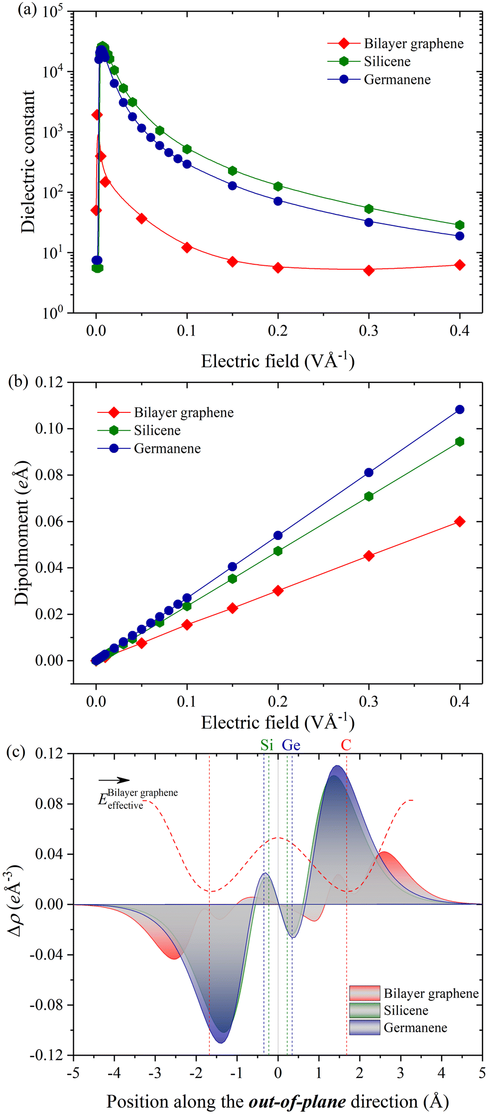 | ||
| Fig. 4 Comparisons among bilayer graphene, monolayer silicene and germanene for (a) the dielectric constant and (b) the dipole moment under a few typical external electric fields. (c) Electric field-induced charge redistribution with respect to the position along the out-of-plane plane, where Δρ = ρ(EZ=0.1) − ρ(EZ=0) and ρ means charge density. | ||
Evidently, there is a similar phenomenon for the charge density distribution (Fig. 4c) of silicene and germanene, which have two peaks with similar values along the positive and negative directions of the z-axis, respectively. A consistent phenomenon can be seen in ESI† Fig. S1. The situation is fundamentally different from bilayer graphene.6,27,54 Taking the positive direction of the z-axis as an example, there is a positive charge accumulation peak, and a negative charge formed a subpeak, both of which are caused by internal charge transfer and induced charge, respectively. The fundamental reason is the destruction of the built-in field and then the rebuilding, which can be traced back to the breaking of inversion symmetry of the structure with the applied external electric field. Thus, the positive charge moves along the positive direction of the z axis, which is identical to the direction of the electric field applied, while the negative charge moves oppositely. The charge transfer caused by the external electric field leads to the generation of internal opposite induced charges (located around the atoms), resulting in a reverse peak with opposite charges. It is intriguing to find that the peaks of the induced charges of monolayer silicene and germanene both appear at the interface of the structure. In contrast, for bilayer graphene, due to the vacuum layer and the weak van der Waals interactions between the two sublayers, the induced charge is deviated, resulting in the unique performance of the charge density and internal effective electric field. It is the special flat structure of AB stacking bilayer graphene that leads to the transfer of electron clouds mainly between layers, as shown in Fig. 4c (more details can be found in ESI† Fig. S1 and S2). Prominently, electron redistribution caused by the applied electric field will eventually increase phonon–phonon scattering and phonon anharmonicity, and further reduce the κ of the AB stacked bilayer graphene, monolayer silicene, and germanene.
4. Conclusion
In summary, the regulation of the thermal transport properties of bilayer graphene, monolayer silicene and germanene were studied by applying an external electric field ranging from 0 to 0.4 V Å−1. The results reveal that the κ of the three materials can be effectively modulated by the external electric field. As the electric field strength increases, κ decreases significantly. Especially, the κ of monolayer germanene can even drop to a record low value of 0.034 W m−1 K−1 when Ez reaches 0.4 V Å−1, which mainly results from the increased phonon–phonon scattering intensity. Combined with the microscopic electronic structure chart, the reconstruction of the internal electric field and the generation of induced charges are the essential reasons for the decrease of κ, which leads to the renormalization of the interaction between atoms. Eventually, phonon–phonon scattering and phonon anharmonicity are affected by the renormalized interatomic interactions, which further leads to the decrease of κ. The strategy of applying an external electric field to manipulate κ as shown in this paper provides a new insight for the design and development of materials with great practical application value. This method can thus be expected to have potential applications in areas such as nanoelectronics, thermoelectrics, and thermal management.Conflicts of interest
There are no conflicts to declare.Acknowledgements
This work is supported by the National Natural Science Foundation of China (Grant No. 52006057), the Fundamental Research Funds for the Central Universities (Grant No. 531119200237 and 541109010001), the Changsha Municipal Natural Science Foundation (Grant No. kq2014034), and the State Key Laboratory of Advanced Design and Manufacturing for Vehicle Body at Hunan University (Grant No. 52175011). Research reported in this publication was also supported in part by the NSF (award number 2030128). The numerical calculations in this paper were conducted on the supercomputing systems of the E. T. Cluster and the National Supercomputing Center in Changsha.References
- K. S. Novoselov, Electric Field Effect in Atomically Thin Carbon Films, Science, 2004, 306, 666–669 CrossRef CAS PubMed
.
- S. Ghosh,
et al., Extremely High Thermal Conductivity of Graphene: Prospects for Thermal Management Applications in Nanoelectronic Circuits, Appl. Phys. Lett., 2008, 92, 151911 CrossRef
- X. Gu and R. Yang, First-principles prediction of phononic thermal conductivity of silicene: A comparison with graphene, J. Appl. Phys., 2015, 117, 025102 CrossRef
- Y. Zhou,
et al., Mechanics of nanoscale wrinkling of graphene on a non-developable surface, Carbon, 2015, 84, 263–271 CrossRef CAS
- Y. Gao, Y. Zhou, X. Zhang and M. Hu, Extremely Low Thermal Conductivity of Polycrystalline Silicene, J. Phys. Chem. C, 2018, 122, 9220–9228 CrossRef CAS
- P. Kumar,
et al., Thickness and electric-field-dependent polarizability and dielectric constant in phosphorene, Phys. Rev. B, 2016, 93, 195428 CrossRef
- Z. Gao, F. Tao and J. Ren, Unusually low thermal conductivity of atomically thin 2D tellurium, Nanoscale, 2018, 10, 12997–13003 RSC
- J.-J. Zhang and S. Dong, Superconductivity of monolayer Mo2C: The key role of functional groups, J. Chem. Phys., 2017, 146, 034705 CrossRef PubMed
- X.-H. Zha,
et al., Intrinsic Structural, Electrical, Thermal, and Mechanical Properties of the Promising Conductor Mo2C MXene, J. Phys. Chem. C, 2016, 120, 15082–15088 CrossRef CAS
- K. H. Yeoh,
et al., First-principles study of monolayer Be2C as an anode material for lithium-ion batteries, J. Appl. Phys., 2019, 126, 125302 CrossRef
- J.-J. Ma, J.-J. Zheng, W.-D. Li, D.-H. Wang and B.-T. Wang, Thermal transport properties of monolayer MoSe 2 with defects, Phys. Chem. Chem. Phys., 2020, 22, 5832–5838 RSC
- W. Sun,
et al., A new 2D monolayer BiXene, M 2 C (M = Mo, Tc, Os), Nanoscale, 2016, 8, 15753–15762 RSC
- H. Xie,
et al., Large tunability of lattice thermal conductivity of monolayer silicene via mechanical strain, Phys. Rev. B, 2016, 93, 075404 CrossRef
- X. Meng,
et al., Thermal Conductivity Enhancement in MoS 2 under Extreme Strain, Phys. Rev. Lett., 2019, 122, 155901 CrossRef CAS PubMed
- Z. Sun,
et al., Disparate strain response of the thermal transport properties of bilayer penta-graphene as compared to that of monolayer penta-graphene, Phys. Chem. Chem. Phys., 2019, 21, 15647–15655 RSC
- M. K. Blees,
et al., Graphene kirigami, Nature, 2015, 524, 204–207 CrossRef CAS PubMed
- J. Bai, X. Zhong, S. Jiang, Y. Huang and X. Duan, Graphene nanomesh, Nat. Nanotechnol., 2010, 5, 190–194 CrossRef CAS PubMed
- Q.-X. Pei, Y.-W. Zhang, Z.-D. Sha and V. B. Shenoy, Tuning the thermal conductivity of silicene with tensile strain and isotopic doping: A molecular dynamics study, J. Appl. Phys., 2013, 114, 033526 CrossRef
- M. Noshin, A. I. Khan, I. A. Navid, H. M. A. Uddin and S. Subrina, Impact of vacancies on the thermal conductivity of graphene nanoribbons: A molecular dynamics simulation study, AIP Adv., 2017, 7, 015112 CrossRef
- Z. Ding, Q.-X. Pei, J.-W. Jiang and Y.-W. Zhang, Manipulating the Thermal Conductivity of Monolayer MoS 2 via Lattice Defect and Strain Engineering, J. Phys. Chem. C, 2015, 119, 16358–16365 CrossRef CAS
- Z. Yan, M. Yoon and S. Kumar, Influence of defects and doping on phonon transport properties of monolayer MoSe2, 2D Mater., 2018, 5, 031008 CrossRef
- W. Ren,
et al., The Impact of Interlayer Rotation on Thermal Transport Across Graphene/Hexagonal Boron Nitride van der Waals Heterostructure, Nano Lett., 2021, 21, 2634–2641 CrossRef CAS PubMed
- X. Zheng, C. Y. Zhao and X. Gu, Thermal conductivity of MoS2/MoSe2 heterostructures: The role of lattice mismatch, interlayer rotation and species intermixing, Int. J. Heat Mass Transfer, 2019, 143, 118583 CrossRef CAS
- H. Li,
et al., Thermal conductivity of twisted bilayer graphene, Nanoscale, 2014, 6, 13402–13408 RSC
- S.-H. Chung, H. Kim and S. W. Jeong, Improved thermal conductivity of carbon-based thermal interface materials by high-magnetic-field alignment, Carbon, 2018, 140, 24–29 CrossRef CAS
- G. Qin, Z. Qin, S.-Y. Yue, Q.-B. Yan and M. Hu, External electric field driving the ultra-low thermal conductivity of silicene, Nanoscale, 2017, 9, 7227–7234 RSC
- E. J. G. Santos and E. Kaxiras, Electric-Field Dependence of the Effective Dielectric Constant in Graphene, Nano Lett., 2013, 13, 898–902 CrossRef CAS PubMed
- Q. Liu,
et al., Tuning Electronic Structure of Bilayer MoS2 by Vertical Electric Field: A First-Principles Investigation, J. Phys. Chem. C, 2012, 116, 21556–21562 CrossRef CAS
- Y. Sun,
et al., Molecular dynamics simulations of the effect of dislocations on the thermal conductivity of iron, J. Appl. Phys., 2020, 127, 045106 CrossRef CAS
- R. Naslain, Design, preparation and properties of non-oxide CMCs for application in engines and nuclear reactors: an overview, Compos. Sci. Technol., 2004, 64, 155–170 CrossRef CAS
- A. Kara,
et al., A review on silicene—New candidate for electronics, Surf. Sci. Rep., 2012, 67, 1–18 CrossRef CAS
- H. Oughaddou,
et al., Silicene, a promising new 2D material, Prog. Surf. Sci., 2015, 90, 46–83 CrossRef CAS
- K. Takeda and K. Shiraishi, Theoretical possibility of stage corrugation in Si and Ge analogs of graphite, Phys. Rev. B: Condens. Matter Mater. Phys., 1994, 50, 14916–14922 CrossRef CAS PubMed
- L. Tao,
et al., Silicene field-effect transistors operating at room temperature, Nat. Nanotechnol., 2015, 10, 227–231 CrossRef CAS PubMed
- B. Mohan, A. Kumar and P. K. Ahluwalia, A first principle study of interband transitions and electron energy loss in mono and bilayer graphene: Effect of external electric field, Phys. E, 2012, 44, 1670–1674 CrossRef CAS
- H. Fu, J. Zhang, Z. Ding, H. Li and S. Meng, Stacking-dependent electronic structure of bilayer silicene, Appl. Phys. Lett., 2014, 104, 131904 CrossRef
- X. Wang and Z. Wu, Intrinsic magnetism and spontaneous band gap opening in bilayer silicene and germanene, Phys. Chem. Chem. Phys., 2017, 19, 2148–2152 RSC
- T. Ohta, A. Bostwick, T. Seyller, K. Horn and E. Rotenberg, Controlling the Electronic Structure of Bilayer Graphene, Science, 2006, 313, 951–954 CrossRef CAS PubMed
- D. Coello-Fiallos,
et al., DFT comparison of structural and electronic properties of graphene and germanene: monolayer and bilayer systems, Mater. Today: Proc., 2017, 4, 6835–6841 Search PubMed
- J. P. Perdew, K. Burke and M. Ernzerhof, Generalized Gradient Approximation Made Simple, Phys. Rev. Lett., 1996, 77, 3865–3868 CrossRef CAS PubMed
- G. Kresse and J. Furthmüller, Efficient iterative schemes for ab initio total-energy calculations using a plane-wave basis set, Phys. Rev. B: Condens. Matter Mater. Phys., 1996, 54, 11169–11186 CrossRef CAS PubMed
- H. J. Monkhorst and J. D. Pack, Special points for Brillouin-zone integrations, Phys. Rev. B: Solid State, 1976, 13, 5188–5192 CrossRef
- A. Togo, F. Oba and I. Tanaka, First-principles calculations of the ferroelastic transition between rutile-type and CaCl2-type SiO2 at high pressures, Phys. Rev. B: Condens. Matter Mater. Phys., 2008, 78, 134106 CrossRef
- K. Esfarjani and H. T. Stokes, Method to extract anharmonic force constants from first principles calculations, Phys. Rev. B: Condens. Matter Mater. Phys., 2008, 77, 144112 CrossRef
- W. Li, J. Carrete, N. A. Katcho and N. Mingo, ShengBTE: A solver of the Boltzmann transport equation for phonons, Comput. Phys. Commun., 2014, 185, 1747–1758 CrossRef CAS
- S. Cahangirov, M. Topsakal, E. Aktürk, H. Şahin and S. Ciraci, Two- and One-Dimensional Honeycomb Structures of Silicon and Germanium, Phys. Rev. Lett., 2009, 102, 236804 CrossRef CAS PubMed
- M. Mirzaei, T. Vazifehshenas, T. Salavati-fard, M. Farmanbar and B. Tanatar, Plasmon-phonon coupling in a valley-spin-polarized two-dimensional electron system: A theoretical study on monolayer silicene, Phys. Rev. B, 2018, 98, 045429 CrossRef CAS
- Md. H. Rahman, E. H. Chowdhury, D. A. Redwan and S. Hong, Computational characterization of thermal and mechanical properties of single and bilayer germanene nanoribbon, Comput. Mater. Sci., 2021, 190, 110272 CrossRef CAS
- B. D. Kong, S. Paul, M. B. Nardelli and K. W. Kim, First-principles analysis of lattice thermal conductivity in monolayer and bilayer graphene, Phys. Rev. B: Condens. Matter Mater. Phys., 2009, 80, 033406 CrossRef
- Z. Zhang,
et al., Heat Conduction Theory Including Phonon Coherence, Phys. Rev. Lett., 2022, 6 DOI:10.1103/PhysRevLett.128.015901
- J. Sun,
et al., Four-Phonon Scattering Effect and Two-Channel Thermal Transport in Two-Dimensional Paraelectric SnSe, ACS Appl. Mater. Interfaces, 2022, 14, 11493–11499 CrossRef CAS PubMed
- N. D. Drummond, V. Zólyomi and V. I. Fal’ko, Electrically tunable band gap in silicene, Phys. Rev. B: Condens. Matter Mater. Phys., 2012, 85, 075423 CrossRef
- Z. Yang, K. Yuan, J. Meng and M. Hu, Electric field tuned anisotropic to isotropic thermal transport transition in monolayer borophene without altering its atomic structure, Nanoscale, 2020, 12, 19178–19190 RSC
- E. J. G. Santos and E. Kaxiras, Electrically Driven Tuning of the Dielectric Constant in MoS2 Layers, ACS Nano, 2013, 7, 10741–10746 CrossRef CAS PubMed
Footnotes |
| † Electronic supplementary information (ESI) available. See DOI: https://doi.org/10.1039/d2cp01117d |
| ‡ These authors contributed equally. |
| This journal is © the Owner Societies 2022 |