
 Open Access Article
 This Open Access Article is licensed under a
 Creative Commons Attribution 3.0 Unported Licence
Lone pair driven anisotropy in antimony chalcogenide semiconductors†
Xinwei
Wang
 a,
Zhenzhu
Li
ab,
Seán R.
Kavanagh
ac,
Alex M.
Ganose
a and
Aron
Walsh
*ab
a,
Zhenzhu
Li
ab,
Seán R.
Kavanagh
ac,
Alex M.
Ganose
a and
Aron
Walsh
*ab
aDepartment of Materials, Imperial College London, Exhibition Road, London SW7 2AZ, UK. E-mail: a.walsh@imperial.ac.uk
bDepartment of Materials Science and Engineering, Yonsei University, Seoul 03722, Korea
cThomas Young Centre and Department of Chemistry, University College London, 20 Gordon Street, London WC1H 0AJ, UK
First published on 9th March 2022
Abstract
Antimony sulfide (Sb2S3) and selenide (Sb2Se3) have emerged as promising earth-abundant alternatives among thin-film photovoltaic compounds. A distinguishing feature of these materials is their anisotropic crystal structures, which are composed of quasi-one-dimensional (1D) [Sb4X6]n ribbons. The interaction between ribbons has been reported to be van der Waals (vdW) in nature and Sb2X3 are thus commonly classified in the literature as 1D semiconductors. However, based on first-principles calculations, here we show that inter-ribbon interactions are present in Sb2X3 beyond the vdW regime. The origin of the anisotropic structures is related to the stereochemical activity of the Sb 5s lone pair according to electronic structure analysis. The impacts of structural anisotropy on the electronic, dielectric and optical properties relevant to solar cells are further examined, including the presence of higher dimensional Fermi surfaces for charge carrier transport. Our study provides guidelines for optimising the performance of Sb2X3-based photovoltaics via device structuring based on the underlying crystal anisotropy.
1 Introduction
Solar photovoltaic (PV) technology which converts the solar energy into electricity provides a clean and sustainable solution to the energy crisis. Current commercial thin-film light absorber materials such as cadmium telluride (CdTe) and copper indium gallium selenide (CIGS) have achieved certified PV efficiencies of over 22% under laboratory conditions.1 These are tetrahedral semiconductors based on expansions of the diamond structure. However, CdTe and CIGS have limitations of the scarcity of the Te element, the toxicity of the Cd element and the high cost of In and Ga elements.2–6As potential alternatives, antimony chalcogenides (Sb2X3; X = S, Se) have attracted growing attention. Their associated ground-state crystal structures are orthorhombic with a range of locally distorted coordination environments. Sb2X3 have advantages of long-term stability, optimal bandgaps and high absorption coefficients (>105 cm−1) with abundant, non-toxic and low-cost constituents.7–9 The PV conversion efficiencies of Sb2X3 devices have increased rapidly during the last decade. The current record efficiencies for pure Sb2S3 and Sb2Se3 have reached 7.5% and 9.2% respectively.10,11 However, these values are still far below the maximum theoretical efficiency of ∼30% predicted by the Shockley–Queisser (SQ) model12 which is an idealised model only based on band gaps of solar absorbers.
Intensive efforts have been devoted to improve the efficiencies in Sb2X3 solar cells. One research direction is the orientation control of Sb2X3 films.13,14 Based on the understanding that Sb2X3 are composed of one-dimensional (1D) [Sb4X6]n ribbons which are held together by vdW forces,15–19 it has been reported that higher PV efficiency could be achieved when the Sb2X3 films are oriented more perpendicular to the substrate due to more efficient carrier transport along ribbons than between them.20 Consequently, researchers have focused on tailoring the growth orientation of Sb2X3 films in order to achieve high efficiencies.11,21–24 However, the origin of anisotropic crystal structures and the connection and the extent of the anisotropy in the physical properties remain unclear. Building on recent work that has shown a tolerance to structural reconstructions,25 understanding how film orientations affect the conversion efficiency in Sb2X3 is crucial to designing high-performance devices.
In this study, we investigate the anisotropic structural, electronic and optical properties of Sb2X3 using first-principles calculations. The dimensionality of Sb2X3 is studied by consideration of the chemical binding energies, carrier effective masses, and Fermi surfaces. Electronic structure analysis further confirms that the orthorhombic crystal structures of Sb2X3 result from the stereochemical activity of the Sb 5s lone pair. Moreover, anisotropic optical properties including dielectric constants and optical absorption spectra are reported.
2 Methods
Analysis of the total energy and electronic structure was performed within the framework of Kohn–Sham density-functional theory (DFT).26,27 Calculations were performed based on DFT as implemented in the Vienna Ab initio Simulation Package (VASP).28 As these materials are non-magnetic, with an even number of electrons, all calculations were spin restricted. The projector augmented-wave (PAW) method29 was employed with a plane-wave energy cutoff of 400 eV. All calculations were carried out using the Heyd–Scuseria–Ernzerhof hybrid functional (HSE06)30,31 except for the calculation of ionic contribution of dielectric constants, as a lower-level functional is sufficient for this high-cost calculation.32To account for the weak inter-ribbon interactions, the optB86b-vdW functional33 was used to calculate the ionic contribution to the static dielectric constant, and the D3 dispersion correction34 was used for HSE06 calculations. The coefficients used for the zero-damping D3 correction are consistent with the previous research.35 In order to obtain well-converged structures, the atomic positions were optimised until the Hellman–Feynman forces on each atom were below 0.0005 eV Å−1, and the energy convergence criterion was set to 10−8 eV. According to convergence tests (shown in Table S2, ESI†), the total energies of Sb2S3 and Sb2Se3 converge to within 1 meV per atom at a k-point mesh of 7 × 2 × 2. Therefore, Γ-centered k-point meshes were set to 7 × 2 × 2 for geometry optimisation with primitive unit cells, and 14 × 4 × 4 for projected density of states (PDOS) and crystal orbital Hamilton populations (COHP) calculations. For calculations of effective masses, dielectric constants and optical absorption coefficients which are more sensitive to k-point density, detailed settings and the proof of convergence are shown in the ESI† (Tables S3–S6).
COHP calculations were performed using the LOBSTER package.36 The conductivity effective mass tensors were calculated by the AMSET package.37 Sb2S3 and Sb2Se3 have complex band structures with multiple band pockets close in energy to the band edges (Fig. S2, ESI†). This means that (i) the high symmetry band structure path does not pass through the true conduction band maximum (CBM) and valence band maximum (VBM) and (ii) picking the effective masses of a single minima/maxima will not be a meaningful metric as multiple band extrema will be occupied even at low temperatures. Therefore, the conventional definitions of effective mass for parabolic bands (such as the curvature effective mass,38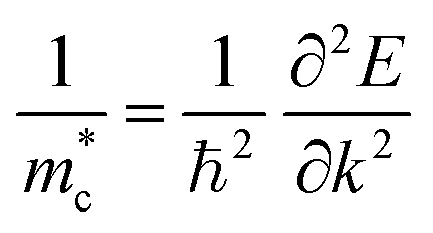 ) are no longer applicable for such systems. The conductivity effective mass (m*) has the advantage that it incorporates effects arising from multiple band extrema and incorporates the full Brillouin zone instead of just the k-points on the high symmetry path. This definition of conductivity effective mass has been widely used to assess materials with complex band structures where the typical picture of effective mass breaks down.39–43 The ionic contribution to the static dielectric constants was calculated by density functional perturbation theory (DFPT),44 while the electronic part was calculated using the approach developed by Furthmüller et al.44 The optical absorption coefficients (α) were calculated from the dielectric function by the sumo package.45 The thickness-dependent radiative limit of solar conversion efficiencies were determined using the calculated optical absorption coefficients, which uses a similar metric to the radiative limit of spectroscopic limited maximum efficiency (SLME).46 We note that excitonic effects are not included in this analysis. More details about the calculations of the effective masses, optical absorption coefficients and radiative limit of solar conversion efficiencies are provided in the ESI.†
The crystal structures and partial charge densities were plotted using CrystalMaker®.47 The PDOS and optical absorption spectra were plotted using the sumo package.45 Fermi surfaces were plotted using the IFermi package.48 The figures of distance histograms, COHP, dielectric constants, optical absorption spectra and thickness-dependent maximum efficiencies were plotted using matplotlib.49
3 Results and discussions
We first consider the anisotropy of the crystal structures found from structural relaxation within DFT, followed by analysis of the orientation-dependence of the associated electronic structure and optical properties.3.1 Structural properties
The ground-state crystal structures of Sb2S3 and Sb2Se3 (Pnma space group) are shown in Fig. 1a. They are composed of strongly bonded quasi-1D [Sb4X6]n ribbons units stacked together by weak interactions. In order to better reproduce the crystal structures, different vdW dispersion correction methods were applied in the geometry optimisation process. Lattice parameters calculated by different functionals and different vdW correction methods and obtained by experiments50–55 are shown in Table 1. The c parameter (the direction between ribbons) is significantly overestimated (>7.0%) with no dispersion correction included for both PBE and HSE06 functionals. Including dispersion corrections, the accuracy of lattice parameter in the c direction is greatly improved regardless of the correction methods. This demonstrates the presence of significant vdW interactions between ribbons, which are much weaker than the bonding within ribbons, and thus the necessity of dispersion corrections when modelling Sb2X3. For both systems, HSE06 + D3 gives the best agreement with experimental measurements (an average difference of 0.7% and 0.9% for Sb2S3 and Sb2Se3 from the experimental lattice constants, respectively), which is in agreement with previous studies,35,56 followed by optB86b performing the next best (1.0% and 1.4% difference for Sb2S3 and Sb2Se3, respectively). Thus, the HSE06 functional with the D3 Grimme dispersion correction was used for most of the following calculations and the optB86b functional was used for most convergence tests.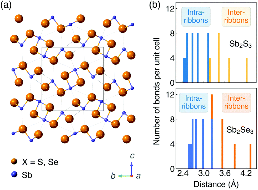 | ||
| Fig. 1 (a) Crystal structures (Pnma space group) and (b) histogram of Sb–X distances of Sb2S3 and Sb2Se3. The unit cell is represented by a rectangle. | ||
| System | PBE | PBE + D3 | PBE + TS | optB86b | HSE06 | HSE06 + D3 | HSE06 + TS | Experimental data | ||||
|---|---|---|---|---|---|---|---|---|---|---|---|---|
| Ref. 50 and 51 | Ref. 52 and 53 | Ref. 54 and 55 | Average | |||||||||
| Sb2S3 | a | 3.87 | 3.84 | 3.88 | 3.86 | 3.80 | 3.80 | 3.81 | 3.84 | 3.82 | 3.84 | 3.83 |
| (1.0) | (0.3) | (1.3) | (0.8) | (−0.8) | (−0.8) | (−0.5) | ||||||
| b | 11.22 | 10.92 | 11.09 | 11.04 | 11.39 | 11.20 | 11.22 | 11.22 | 11.27 | 11.29 | 11.26 | |
| (−0.4) | (−3.1) | (−1.5) | (−2.0) | (1.1) | (−0.5) | (−0.4) | ||||||
| c | 12.14 | 11.15 | 11.54 | 11.32 | 12.09 | 11.39 | 11.54 | 11.31 | 11.30 | 11.27 | 11.29 | |
| (7.0) | (−1.3) | (2.2) | (0.3) | (6.6) | (0.9) | (2.2) | ||||||
| Sb2Se3 | a | 4.03 | 3.99 | 4.04 | 4.02 | 3.96 | 3.95 | 3.97 | 3.98 | 3.99 | 3.96 | 3.98 |
| (1.2) | (0.3) | (1.5) | (1.0) | (−0.5) | (−0.8) | (−0.3) | ||||||
| b | 11.53 | 11.33 | 11.41 | 11.46 | 11.73 | 11.55 | 11.54 | 11.65 | 11.65 | 11.62 | 11.64 | |
| (−1.0) | (−2.7) | (−2.0) | (−1.6) | (0.8) | (−0.8) | (−0.9) | ||||||
| c | 12.84 | 11.68 | 12.31 | 11.90 | 12.65 | 11.93 | 12.18 | 11.80 | 11.79 | 11.77 | 11.79 | |
| (8.2) | (−0.9) | (4.2) | (0.9) | (6.8) | (1.2) | (3.2) | ||||||
Histograms of distances between Sb and X ions are shown in Fig. 1b. The widely distributed bond lengths indicate the anisotropic connectivity of Sb2X3. The bond lengths of Sb2Se3 are slightly larger than those of Sb2S3 due to the increased anion radius. In the study of Deringer et al.,57 analysis of the integrated COHP and the harmonic force constants showed a clear separation between strong intra-ribbon and weaker inter-ribbon interactions in Sb2Se3. In order to quantify the interaction between ribbons, inter-ribbon binding energies per atom (Eb) and binding energies per bond along the b (Eb(b)) and c (Eb(c)) directions are calculated by
| Eb = (2E2D − Et)/20 | (1) |
| Eb(b) = (E1D − E2D)/2 | (2) |
| Eb(c) = (2E2D − Et)/16 | (3) |
| System | E b | E b(b) | E b(c) |
|---|---|---|---|
| Sb2S3 | 12.77 | 27.44 | 15.96 |
| Sb2Se3 | 14.36 | 31.13 | 17.95 |
3.2 Electronic properties
The strength of the interaction between ribbons is closely related to the distortion of Sb atomic environment which originates from the stereochemically active Sb 5s lone pairs. Before going further into the lone pair analysis, the density of states and orbital overlaps are first investigated.The PDOS are shown in Fig. 2a and b. The valence band (VB) can be divided into two main parts. The highest occupied VB between −1 and 0 eV consists of S 3p/Se 4p, Sb 5s and Sb 5p states. While the states between −10 and −7 eV mainly consists of Sb 5s orbitals, alongside some small contributions from S 3s/Se 4s and S 3p/Se 4p states. A valley at about 2 eV below the valence band maximum (VBM) is demonstrated to be one of the major characteristics of energy distribution curves for Sb2Se3 according to the photoemission measurements.55 Our calculated PDOS of Sb2Se3 also shows a valley at ∼−2 eV which is in good agreement with the experimental results. The conduction band (CB) are dominated by Sb 5p and S 3p/Se 4p states. These results agree well with earlier studies of PDOS on Sb2X3.57,64–66
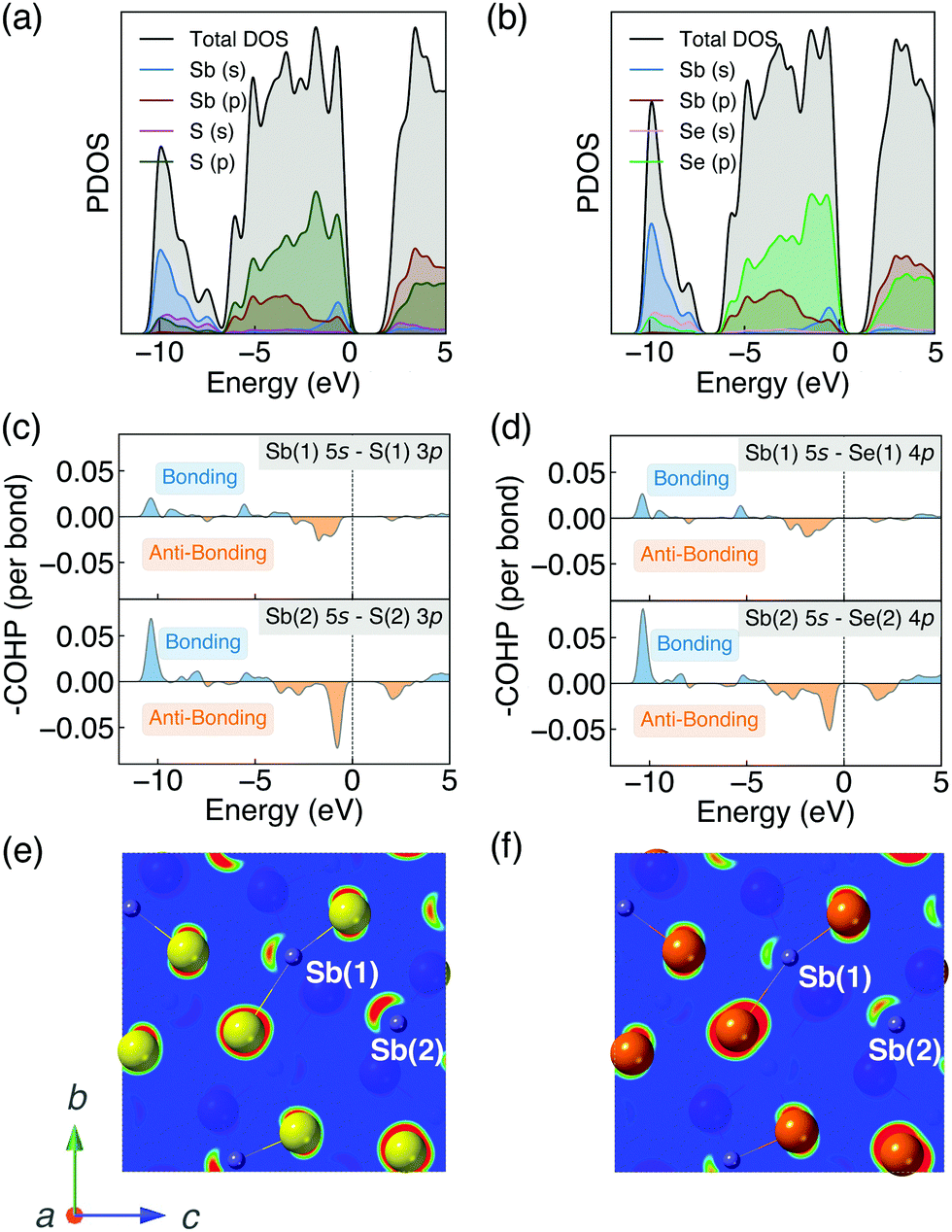 | ||
| Fig. 2 (a) and (b) Projected density of states (PDOS), (c) and (d) crystal orbital Hamilton populations (COHP) and (e) and (f) partial charge densities of antimony chacogenides. The range of isosurface value for partial charge densities is set to 0.05–0.10 e Å−3 for both Sb2S3 and Sb2Se3. The VBM is set to 0 in each case. | ||
The bonding and antibonding interactions are further studied by COHP36 (shown in Fig. 2c and d). Two separate cases are plotted since Sb has two distinct chemical environments. The interaction is weaker in Sb(1)–X(1) than Sb(2)–X(2) which agrees with the longer bond lengths of Sb(1)–X(1). Combined with the results of PDOS, the energy range from −10 to −7 eV corresponds to a bonding interaction between Sb 5s and S 3p/Se 4p states, whereas the region at the top of the VB corresponds to an antibonding state, which is similar to other quasi-1D systems with stereochemically active lone pairs.67 The photoemission measurements for Sb2Se355 show that the lower part of VB below ∼−6 eV is contributed by bonding states which agrees well with our results. Moreover, the interaction is stronger in Sb2S3 than Sb2Se3 which will be discussed in detail later.
The different inter-ribbon interactions in Sb2S3 and Sb2Se3 result from the Sb 5s lone pair formation. In the revised lone pair model,68 the interaction between the antibonding states of cation s–anion p and cation p states results in the formation of stereochemically active lone pairs. Smaller energy difference between cation s and anion p states will facilitate stronger interaction and thus a more asymmetric electron density. In our systems, for the Sb(III) oxidation state found in Sb2X3, the formal electronic configuration of Sb is 5s25p0. Based on the discussions above, the Sb 5s states interact with the S 3p/Se 4p states in the VB forming filled bonding and antibonding states. The additional interaction of the nominally empty Sb 5p orbitals stabilises the system by lowering the total energy, which is similar to other lone pair systems.68–71 The resulting stereochemically active lone pair results in an asymmetric electronic density at the top of VB which can be visualised by the contour plot of partial charge density. Partial charge densities for the states between −1 and 0 eV (with respect to the VBM) are shown in Fig. 2e and f. They are obtained by cutting the (100) plane through Sb atoms. The lone pair is stronger in Sb2S3 compared with Sb2Se3 due to the smaller energy separation and increased overlap of Sb 5s and S 3p.
To connect the electronic structure to transport properties, effective masses of electrons and holes were calculated (shown in Table 3). According to the electronic band structures of Sb2S3 and Sb2Se3 (shown in Fig. S2, ESI†), the band dispersions around the extrema are relatively flat which are far from parabolic. Therefore, effective masses in Sb2X3 are quite sensitive to calculation parameters (particularly the k-point density), and effective masses larger than 2 are rounded to the nearest whole numbers in Table 3 and Table S3 (ESI†). The harmonic mean is used to average the values for a polycrystalline sample with random orientations, and the anisotropy ratio (ar) is defined as the ratio of maximum to minimum effective mass. The average effective masses of holes are larger than those of electrons for both Sb2S3 and Sb2Se3, indicating that Sb2S3 and Sb2Se3 may be better n-type semiconductors. Nevertheless, the electron effective masses show a stronger anisotropy. ar is larger in Sb2Se3 than Sb2S3 for both electron and hole effective masses, suggesting Sb2Se3 has stronger anisotropy which agrees with the weaker lone pair and longer bond lengths in Sb2Se3. The electron and hole effective masses are the largest along [001] for both Sb2S3 and Sb2Se3, indicating the conductivity along [001] will be lower than along the other two directions. This is also consistent with the low inter-ribbon binding energies along the [001] direction and the direction of the Sb 5s lone pair (Fig. 2e and f). In general the values follow the trend x < y < z, with the exception of the hole effective mass for Sb2Se3, which is discussed later. Moreover, the 2D nature of transport (with small effective masses in two directions and large effective mass in the other direction) is similar to other so-called “quasi-1D” systems such as BiSI and BiSeI.72 Our calculated effective masses deviate largely from other studies on Sb2X3.73,74 One possible reason of the discrepancy could be the use of simple parabolic fitting or the consideration of solely the Γ point in other computational investigations. The choice of functionals could be another important factor, as demonstrated by Whalley et al.75 It has been demonstrated that semi-local functionals would not only underestimate the bandgap, but also would influence the shape of band structures, resulting in overestimated nonparabolicity.
![[m with combining macron]](https://www.rsc.org/images/entities/i_char_006d_0304.gif) *. The anisotropy ratio (ar) is defined as the ratio of maximum to minimum effective mass
*. The anisotropy ratio (ar) is defined as the ratio of maximum to minimum effective mass
| System | x | y | z |
* |
a r | |
|---|---|---|---|---|---|---|
| Sb2S3 |
|
0.16 | 0.92 | 5 | 0.40 | 31.25 |
|
0.47 | 0.65 | 0.97 | 0.64 | 2.06 | |
| Sb2Se3 |

|
0.14 | 0.81 | 7 | 0.35 | 50.00 |

|
0.85 | 0.55 | 3 | 0.90 | 5.45 |
To further illustrate the dimensionality of the electronic structure, Fermi surfaces were plotted at 0.1 eV below (above) the VBM (CBM) using the IFermi package48 (shown in Fig. 3). 0.1 eV is an arbitrary value intended to indicate the shape of the Fermi surface close to the band edge. Due to the tails of the Fermi–Dirac distribution, this energy range will be occupied at room temperature and the Fermi surface is therefore reflective of the states that govern transport properties. The Fermi surfaces of 0.08 and 0.12 eV below (above) the VBM (CBM) were also shown in Fig. S3 and S4 (ESI†) which qualitatively show the same behaviour. An ellipsoidal Fermi surface is found for holes in Sb2S3 (Fig. 3a), indicating dispersion in three dimensions.76,77 The shape of warped cylinders (considering the periodic boundary conditions) found for electrons in Sb2S3 (Fig. 3c) can be classified as quasi-2D with small dispersion in the [001] direction.76,77 These agree well with observation that the hole effective mass of Sb2S3 is much smaller than the electron effective mass in the [001] direction. In contrast, for Sb2Se3, due to the relatively large hole and electron effective masses in the [001] direction, the hole and electron Fermi surfaces of Sb2Se3 are quasi-2D (with the shape of warped cylinders) (shown in Fig. 3b and d). Moreover, it can be seen that the electron Fermi surfaces of Sb2S3 and Sb2Se3 have similar topology, which is consistent with the similar values of effective masses and indicates similar transport behaviours, whereas their hole Fermi surfaces have a significant difference in terms of the dimensionality. Indeed, for Sb2S3 the three components of the effective masses are all below one, while for Sb2Se3 the z component is greater than 3. We link this behaviour to the stronger lone pair distortion of Sb2S3 and the resulting shorter inter-ribbon Sb–S bonds along the [001] direction.
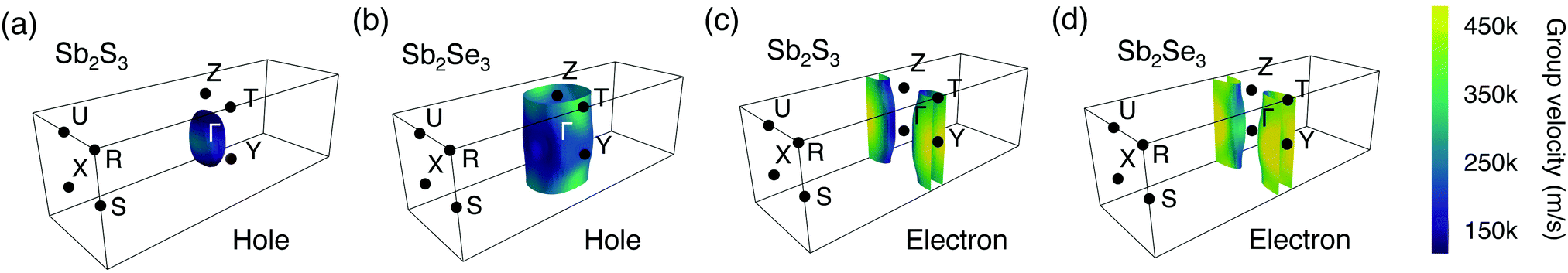 | ||
| Fig. 3 Fermi surfaces of Sb2S3 and Sb2Se3. (a) and (c) are hole Fermi surfaces (0.1 eV below the valence band maximum), while (b) and (d) are electron Fermi surfaces (0.1 eV above the conduction band minimum). The different colors represent the magnitude of group velocity (m s−1). | ||
3.3 Optical properties
The dielectric constants are important descriptors for the optical properties of crystals. The static dielectric constant (ε0) is defined as the sum of the ionic and high-frequency response to an external electric field. The complex dielectric function ε(ω) is given by:| ε(ω) = ε1(ω) + iε2(ω) | (4) |
| System | ε 0 | ε ∞ | ||||||
|---|---|---|---|---|---|---|---|---|
| x | y | z | a r | x | y | z | a r | |
| Sb2S3 | 98.94 | 94.21 | 13.14 | 7.53 | 11.55 | 10.97 | 8.25 | 1.40 |
| Sb2Se3 | 85.64 | 128.18 | 15.00 | 8.54 | 15.11 | 14.92 | 10.53 | 1.43 |
The real and imaginary parts of the high-frequency (ε∞) dielectric functions are plotted in Fig. 4. Combined with the results of PDOS, the peaks in the imaginary parts of dielectric functions mainly correspond to the optical transition from the S 3p/Se 4p states in the valence band to the Sb 5p states in the conduction band. Our calculated dielectric constants are in excellent agreement with ellipsometry measurements on polycrystalline thin films (ε∞,x, ε∞,y and ε∞,z of 12.5, 10.8 and 7.0 for Sb2S3,81 respectively, and an averaged ε∞ of 14.3 for Sb2Se37). Furthermore, our results are inline with previous theoretical studies.65,82–85
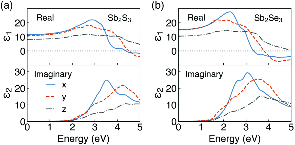 | ||
| Fig. 4 Calculated high-frequency dielectric functions of (a) Sb2S3 and (b) Sb2Se3. | ||
The calculated optical absorption spectra, and radiative limit of solar conversion efficiency, for Sb2S3 and Sb2Se3 are shown in Fig. 5. As can be seen in Fig. 5a, both Sb2S3 and Sb2Se3 possess high optical absorption coefficients above the band edge (in the range of 105 cm−1) which could more effectively absorb photons and generate electron–hole pairs. This agrees well with experimental UV-vis measurements on Sb2X3, which observed large absorption coefficients of ∼105 cm−1 in the visible region.2,9,86,87 Possible reasons for such high optical absorption coefficients in these indirect gap semiconductors could be attributed to their unique electronic band structures (shown in Fig. S2, ESI†). On the one hand, the difference between indirect and direct gaps of Sb2X3 is small (0.16 eV for Sb2S3 and 0.06 eV for Sb2Se3) which makes them still suitable for strong absorption near the band edges.88 On the other hand, the relatively flat dispersions near the band extrema will lead to high DOS near the VBM and CBM and thus strong absorption.89 Moreover, there is slight difference in absorption coefficients along different directions. The thickness-dependent radiative limit of conversion efficiencies (Fig. 5b) along different orientations were further determined using the calculated optical absorption coefficients. The efficiencies show a strong dependence on the film thickness in the 0–2 μm range, and rise rapidly with the increase of the film thickness due to the large magnitude of optical absorption coefficients. We note that our simplified model assumes that all generated carriers are collected, which means the mobility is assumed to be infinitely high. Under this assumption, for both Sb2S3 and Sb2Se3, the radiative limit of efficiencies approach the SQ limit at a thickness of 2 μm. Within our model, which incorporates the electronic structure and direction-dependent optical absorption, the solar conversion efficiencies are equivalent in each different orientation. The efficiencies are larger in Sb2Se3 than Sb2S3 since the band gap of Sb2Se3 is closer to the optimal band gap predicted by the SQ model. These results indicate that absorption does not lead to orientation dependence in the conversion efficiencies in Sb2S3 and Sb2Se3. We note that our predictions of anisotropic crystal structure and anisotropic effective masses indicate that real devices will likely show orientation-dependent efficiencies, due to favourable (benign) grain boundary orientations20 and anisotropic carrier mobilities (and thus charge collection efficiencies). Beyond this, the presence of defects in Sb2X310,35,56,90–93 also reduces conversion efficiencies from the idealised theoretical limit to that obtained in real devices.
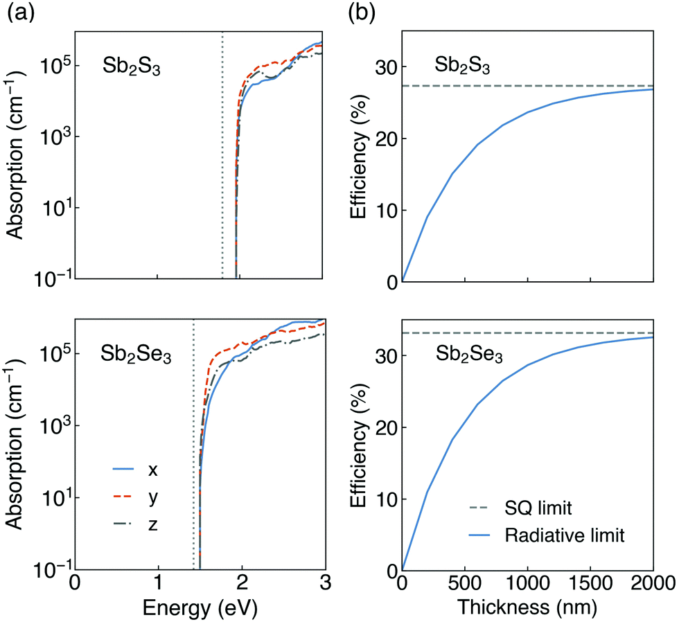 | ||
| Fig. 5 (a) Calculated optical absorption spectra of Sb2S3 and Sb2Se3 arising from direct valence to conduction band transitions. The fundamental band gaps are shown in grey dotted lines. (b) Thickness-dependent maximum efficiencies based on the radiative limit of Sb2S3 and Sb2Se3. | ||
4 Conclusions
The standard description of Sb2X3 in the literature refers to them as 1D semiconductors, where electrons and holes can readily diffuse along, but not between, ribbons in the crystal. This has lead to a focus on thin-film synthesis to achieve optimal [100] orientations. Our first-principles investigation has shown that the chemical binding energies between ribbons (>10 kJ mol−1) fall between the vdW and ionic/covalent regime. Analysis of the carrier effective masses does reveal a strong anisotropy, but the behaviour is not 1D, with stronger dispersion found in [010] compared to [001]. The Fermi surfaces for electrons and holes illustrate this complexity with a combination of 3D (holes in Sb2S3) and quasi-2D transport. The anisotropy carries through to the dielectric response of the crystals with much stronger screening in the ab plane compared to along the c axis. However, the resulting optical absorption profiles are less sensitive and yield the same radiative limit of conversion efficiencies for photovoltaic applications. The origin of these anisotropic effects is linked to lone pair formation associated with the filled Sb 5s orbitals which distorts the Sb coordination environment. Beyond the bulk crystal properties, the orientation-dependence should extend to the crystal terminations where the associated surface polarisation will influence electron and hole extraction by electrical contacts.Conflicts of interest
There are no conflicts to declare.Acknowledgements
We are grateful to the UK Materials and Molecular Modelling Hub for computational resources, which is partially funded by EPSRC (EP/P020194/1 and EP/T022213/1). Xinwei Wang acknowledges Imperial College London for the funding of a President's PhD Scholarship. Seán R. Kavanagh acknowledges the EPSRC Centre for Doctoral Training in the Advanced Characterisation of Materials (CDT-ACM) (EP/S023259/1) for funding a PhD studentship. Alex M. Ganose was supported by EPSRC Fellowship EP/T033231/1. Xinwei Wang thanks Chengcheng Xiao and Sunghyun Kim for advice on the computational analysis.References
- M. A. Green, E. D. Dunlop, J. Hohl-Ebinger, M. Yoshita, N. Kopidakis and A. W. Ho-Baillie, Prog. Photovolt. Res. Appl., 2020, 28, 3–15 CrossRef.
- K. Zeng, D.-J. Xue and J. Tang, Semicond. Sci. Technol., 2016, 31, 063001 CrossRef.
- H. Lei, J. Chen, Z. Tan and G. Fang, Sol. RRL, 2019, 3, 1900026 CrossRef.
- R. Kondrotas, C. Chen and J. Tang, Joule, 2018, 2, 857–878 CrossRef CAS.
- A. Mavlonov, T. Razykov, F. Raziq, J. Gan, J. Chantana, Y. Kawano, T. Nishimura, H. Wei, A. Zakutayev and T. Minemoto, et al. , Sol. Energy, 2020, 201, 227–246 CrossRef CAS.
- J. T. Dufton, A. Walsh, P. M. Panchmatia, L. M. Peter, D. Colombara and M. S. Islam, Phys. Chem. Chem. Phys., 2012, 14, 7229–7233 RSC.
- C. Chen, W. Li, Y. Zhou, C. Chen, M. Luo, X. Liu, K. Zeng, B. Yang, C. Zhang and J. Han, et al. , Appl. Phys. Lett., 2015, 107, 043905 CrossRef.
- C. Ghosh and B. Varma, Thin Solid Films, 1979, 60, 61–65 CrossRef CAS.
- Y. Zhou, M. Leng, Z. Xia, J. Zhong, H. Song, X. Liu, B. Yang, J. Zhang, J. Chen and K. Zhou, et al. , Adv. Energy Mater., 2014, 4, 1301846 CrossRef.
- Y. C. Choi, D. U. Lee, J. H. Noh, E. K. Kim and S. I. Seok, Adv. Funct. Mater., 2014, 24, 3587–3592 CrossRef CAS.
- Z. Li, X. Liang, G. Li, H. Liu, H. Zhang, J. Guo, J. Chen, K. Shen, X. San and W. Yu, et al. , Nat. Commun., 2019, 10, 1–9 CrossRef PubMed.
- W. Shockley and H. J. Queisser, J. Appl. Phys., 1961, 32, 510–519 CrossRef CAS.
- J. Kim, S. Ji, Y. Jang, G. Jeong, J. Choi, D. Kim, S.-W. Nam and B. Shin, Sol. RRL, 2021, 5, 2100327 CrossRef CAS.
- T. D. Hobson, L. J. Phillips, O. S. Hutter, H. Shiel, J. E. Swallow, C. N. Savory, P. K. Nayak, S. Mariotti, B. Das and L. Bowen, et al. , Chem. Mater., 2020, 32, 2621–2630 CrossRef CAS.
- F. Caruso, M. R. Filip and F. Giustino, Phys. Rev. B, 2015, 92, 125134 CrossRef.
- H. Song, T. Li, J. Zhang, Y. Zhou, J. Luo, C. Chen, B. Yang, C. Ge, Y. Wu and J. Tang, Adv. Mater., 2017, 29, 1700441 CrossRef PubMed.
- L. Guo, B. Zhang, Y. Qin, D. Li, L. Li, X. Qian and F. Yan, Sol. RRL, 2018, 2, 1800128 CrossRef.
- W. Yang, J. Ahn, Y. Oh, J. Tan, H. Lee, J. Park, H.-C. Kwon, J. Kim, W. Jo and J. Kim, et al. , Adv. Energy Mater., 2018, 8, 1702888 CrossRef.
- R. Gusmão, Z. Sofer, J. Luxa and M. Pumera, ACS Sustain. Chem. Eng., 2019, 7, 15790–15798 CrossRef.
- Y. Zhou, L. Wang, S. Chen, S. Qin, X. Liu, J. Chen, D.-J. Xue, M. Luo, Y. Cao and Y. Cheng, et al. , Nat. Photonics, 2015, 9, 409–415 CrossRef CAS.
- S. Yuan, H. Deng, D. Dong, X. Yang, K. Qiao, C. Hu, H. Song, H. Song, Z. He and J. Tang, Sol. Energy Mater. Sol. Cells, 2016, 157, 887–893 CrossRef CAS.
- L. Wang, D.-B. Li, K. Li, C. Chen, H.-X. Deng, L. Gao, Y. Zhao, F. Jiang, L. Li and F. Huang, et al. , Nat. Energy, 2017, 2, 1–9 Search PubMed.
- R. Kondrotas, J. Zhang, C. Wang and J. Tang, Sol. Energy Mater. Sol. Cells, 2019, 199, 16–23 CrossRef CAS.
- Y. Zeng, K. Sun, J. Huang, M. P. Nielsen, F. Ji, C. Sha, S. Yuan, X. Zhang, C. Yan and X. Liu, et al. , ACS Appl. Mater. Interfaces, 2020, 12, 22825–22834 CrossRef CAS PubMed.
- K. P. McKenna, Adv. Electron. Mater., 2021, 7, 2000908 CrossRef CAS.
- W. Kohn and L. J. Sham, Phys. Rev., 1965, 140, A1133 CrossRef.
- R. M. Dreizler and E. K. Gross, Density Functional Theory, Springer, 1990, pp. 245–271 Search PubMed.
- G. Kresse and J. Furthmüller, Phys. Rev. B: Condens. Matter Mater. Phys., 1996, 54, 11169 CrossRef CAS PubMed.
- G. Kresse and D. Joubert, Phys. Rev. B: Condens. Matter Mater. Phys., 1999, 59, 1758 CrossRef CAS.
- J. Heyd, G. E. Scuseria and M. Ernzerhof, J. Chem. Phys., 2003, 118, 8207–8215 CrossRef CAS.
- A. V. Krukau, O. A. Vydrov, A. F. Izmaylov and G. E. Scuseria, J. Chem. Phys., 2006, 125, 224106 CrossRef PubMed.
- S. R. Kavanagh, A. Walsh and D. O. Scanlon, ACS Energy Lett., 2021, 6, 1392–1398 CrossRef CAS PubMed.
- J. Klimeš, D. R. Bowler and A. Michaelides, Phys. Rev. B: Condens. Matter Mater. Phys., 2011, 83, 195131 CrossRef.
- S. Grimme, J. Comput. Chem., 2004, 25, 1463–1473 CrossRef CAS PubMed.
- C. N. Savory and D. O. Scanlon, J. Mater. Chem. A, 2019, 7, 10739–10744 RSC.
- R. Dronskowski and P. E. Blöchl, J. Phys. Chem., 1993, 97, 8617–8624 CrossRef CAS.
- A. M. Ganose, J. Park, A. Faghaninia, R. Woods-Robinson, K. A. Persson and A. Jain, Nat. Commun., 2021, 12, 1–9 CrossRef PubMed.
- N. W. Ashcroft and N. D. Mermin, Solid State Physics, Harcourt College Publishers, Fort Worth, 1976 Search PubMed.
- G. Hautier, A. Miglio, G. Ceder, G.-M. Rignanese and X. Gonze, Nat. Commun., 2013, 4, 1–7 Search PubMed.
- G. Hautier, A. Miglio, D. Waroquiers, G.-M. Rignanese and X. Gonze, Chem. Mater., 2014, 26, 5447–5458 CrossRef CAS.
- A. Bhatia, G. Hautier, T. Nilgianskul, A. Miglio, J. Sun, H. J. Kim, K. H. Kim, S. Chen, G.-M. Rignanese and X. Gonze, et al. , Chem. Mater., 2016, 28, 30–34 CrossRef CAS.
- L. Lykke, B. B. Iversen and G. K. Madsen, Phys. Rev. B: Condens. Matter Mater. Phys., 2006, 73, 195121 CrossRef.
- D. S. Parker, A. F. May and D. J. Singh, Phys. Rev. Appl., 2015, 3, 064003 CrossRef.
- M. Gajdoš, K. Hummer, G. Kresse, J. Furthmüller and F. Bechstedt, Phys. Rev. B: Condens. Matter Mater. Phys., 2006, 73, 045112 CrossRef.
- A. M. Ganose, A. J. Jackson and D. O. Scanlon, J. Open Source Softw., 2018, 3, 717 CrossRef.
- L. Yu and A. Zunger, Phys. Rev. Lett., 2012, 108, 068701 CrossRef PubMed.
- CrystalMaker, CrystalMaker Software Ltd, Oxford, England, (http://www.crystalmaker.com).
- A. M. Ganose, A. Searle, A. Jain and S. M. Griffin, J. Open Source Softw., 2021, 6, 3089 CrossRef.
- J. D. Hunter, Comput. Sci. Eng., 2007, 9, 90–95 Search PubMed.
- A. Kyono, M. Kimata, M. Matsuhisa, Y. Miyashita and K. Okamoto, Phys. Chem. Miner., 2002, 29, 254–260 CrossRef CAS.
- O. Savadogo and K. Mandal, Sol. Energy Mater. Sol. Cells, 1992, 26, 117–136 CrossRef CAS.
- A. Salem and M. S. Selim, J. Phys. D, 2001, 34, 12 CrossRef CAS.
- I. Efthimiopoulos, J. Zhang, M. Kucway, C. Park, R. C. Ewing and Y. Wang, Sci. Rep., 2013, 3, 1–8 Search PubMed.
- G. Voutsas, A. Papazoglou, P. Rentzeperis and D. Siapkas, Z. Kristallogr. Cryst. Mater., 1985, 171, 261–268 CrossRef CAS.
- Z. Hurych, D. Davis, D. Buczek, C. Wood, G. Lapeyre and A. Baer, Phys. Rev. B: Condens. Matter Mater. Phys., 1974, 9, 4392 CrossRef CAS.
- A. Stoliaroff, A. Lecomte, O. Rubel, S. Jobic, X. Zhang, C. Latouche and X. Rocquefelte, ACS Appl. Energy Mater., 2020, 3, 2496–2509 CrossRef CAS.
- V. L. Deringer, R. P. Stoffel, M. Wuttig and R. Dronskowski, Chem. Sci., 2015, 6, 5255–5262 RSC.
- N. Mounet, M. Gibertini, P. Schwaller, D. Campi, A. Merkys, A. Marrazzo, T. Sohier, I. E. Castelli, A. Cepellotti and G. Pizzi, et al. , Nat. Nanotechnol., 2018, 13, 246–252 CrossRef CAS PubMed.
- T. Björkman, A. Gulans, A. V. Krasheninnikov and R. M. Nieminen, Phys. Rev. Lett., 2012, 108, 235502 CrossRef PubMed.
- R. H. Garrett and C. M. Grisham, Biochemistry, Brooks/Cole, Boston, 2010 Search PubMed.
- M. R. Filip, C. E. Patrick and F. Giustino, Phys. Rev. B: Condens. Matter Mater. Phys., 2013, 87, 205125 CrossRef.
- L. Xian, A. P. Paz, E. Bianco, P. M. Ajayan and A. Rubio, 2D Mater., 2017, 4, 041003 CrossRef.
- D. Wines, J. A. Kropp, G. Chaney, F. Ersan and C. Ataca, Phys. Chem. Chem. Phys., 2020, 22, 6727–6737 RSC.
- R. Caracas and X. Gonze, Phys. Chem. Miner., 2005, 32, 295–300 CrossRef CAS.
- H. Koç, A. M. Mamedov, E. Deligoz and H. Ozisik, Solid State Sci., 2012, 14, 1211–1220 CrossRef.
- A. Radzwan, R. Ahmed, A. Shaari, A. Lawal and Y. X. Ng, Malays. J. Fundam. Appl. Sci., 2017, 13, 285–289 Search PubMed.
- A. M. Ganose, K. T. Butler, A. Walsh and D. O. Scanlon, J. Mater. Chem. A, 2016, 4, 2060–2068 RSC.
- A. Walsh, D. J. Payne, R. G. Egdell and G. W. Watson, Chem. Soc. Rev., 2011, 40, 4455–4463 RSC.
- A. Walsh and G. W. Watson, J. Solid State Chem., 2005, 178, 1422–1428 CrossRef CAS.
- J. P. Allen, J. J. Carey, A. Walsh, D. O. Scanlon and G. W. Watson, J. Phys. Chem. C, 2013, 117, 14759–14769 CrossRef CAS.
- S. R. Kavanagh, C. N. Savory, D. O. Scanlon and A. Walsh, Mater. Horiz., 2021, 8, 2709–2716 RSC.
- A. M. Ganose, S. Matsumoto, J. Buckeridge and D. O. Scanlon, Chem. Mater., 2018, 30, 3827–3835 CrossRef CAS PubMed.
- T. B. Nasr, H. Maghraoui-Meherzi and N. Kamoun-Turki, J. Alloys Compd., 2016, 663, 123–127 CrossRef.
- W. Qiu, C. Zhang, S. Cheng, Q. Zheng, X. Yu, H. Jia and B. Wu, J. Solid State Chem., 2019, 271, 339–345 CrossRef CAS.
- L. D. Whalley, J. M. Frost, B. J. Morgan and A. Walsh, Phys. Rev. B, 2019, 99, 085207 CrossRef CAS.
- I. Matsuda and S. Hasegawa, J. Phys.: Condens. Matter, 2007, 19, 355007 CrossRef.
- S. G. Albert, PhD thesis, Technische Universität München, 2015.
- A. Walsh and A. Zunger, Nat. Mater., 2017, 16, 964–967 CrossRef CAS PubMed.
- Y. Liu, K. T. E. Chua, T. C. Sum and C. K. Gan, Phys. Chem. Chem. Phys., 2014, 16, 345–350 RSC.
- Y. Cheng, O. Cojocaru-Mirédin, J. Keutgen, Y. Yu, M. Küpers, M. Schumacher, P. Golub, J.-Y. Raty, R. Dronskowski and M. Wuttig, Adv. Mater., 2019, 31, 1904316 CrossRef CAS PubMed.
- M. Schubert, T. Hofmann, C. Herzinger and W. Dollase, Thin Solid Films, 2004, 455, 619–623 CrossRef.
- T. B. Nasr, H. Maghraoui-Meherzi, H. B. Abdallah and R. Bennaceur, Phys. B, 2011, 406, 287–292 CrossRef.
- M. H. Lakhdar, B. Ouni and M. Amlouk, Mater. Sci. Semicond. Process., 2014, 19, 32–39 CrossRef.
- H. Maghraoui-Meherzi, T. B. Nasr and M. Dachraoui, Mater. Sci. Semicond. Process., 2013, 16, 179–184 CrossRef CAS.
- A. Lawal, A. Shaari, R. Ahmed and L. Taura, Curr. Appl. Phys., 2018, 18, 567–575 CrossRef.
- M. Y. Versavel and J. A. Haber, Thin Solid Films, 2007, 515, 7171–7176 CrossRef CAS.
- Y. Lai, Z. Chen, C. Han, L. Jiang, F. Liu, J. Li and Y. Liu, Appl. Surf. Sci., 2012, 261, 510–514 CrossRef CAS.
- R. Kondrotas, C. Chen, X. Liu, B. Yang and J. Tang, J. Semicond., 2021, 42, 031701 CrossRef CAS.
- M. Kumar, N. Umezawa and M. Imai, Appl. Phys. Express, 2014, 7, 071203 CrossRef CAS.
- X. Liu, X. Xiao, Y. Yang, D.-J. Xue, D.-B. Li, C. Chen, S. Lu, L. Gao, Y. He and M. C. Beard, et al. , Prog. Photovolt., 2017, 25, 861–870 CrossRef CAS.
- X. Hu, J. Tao, G. Weng, J. Jiang, S. Chen, Z. Zhu and J. Chu, Sol. Energy Mater. Sol. Cells, 2018, 186, 324–329 CrossRef CAS.
- Z. Cai, C.-M. Dai and S. Chen, Sol. RRL, 2020, 4, 1900503 CrossRef CAS.
- M. Huang, Z. Cai, S. Wang, X.-G. Gong, S.-H. Wei and S. Chen, Small, 2021, 17, 2102429 CrossRef CAS PubMed.
Footnote |
| † Electronic supplementary information (ESI) available. See DOI: 10.1039/d1cp05373f |
| This journal is © the Owner Societies 2022 |