
 Open Access Article
 This Open Access Article is licensed under a Creative Commons Attribution-Non Commercial 3.0 Unported Licence
Electronic structures of the MoS2/TiO2 (anatase) heterojunction: influence of physical and chemical modifications at the 2D- or 1D-interfaces†
Rémi
Favre
 a,
Pascal
Raybaud
*ab and
Tangui
Le Bahers
*a
a,
Pascal
Raybaud
*ab and
Tangui
Le Bahers
*a
aUniv Lyon, ENS de Lyon, CNRS, Université Claude Bernard Lyon 1, Laboratoire de Chimie UMR 5182, F-69342, France. E-mail: pascal.raybaud@ifpen.fr; tangui.le_bahers@ens-lyon.fr
bIFP Energies Nouvelles, Rond-point de l’échangeur de Solaize, BP 3, 69360 Solaize, France
First published on 4th January 2022
Abstract
To tackle the challenge of CO2 photoreduction, semiconducting layered transition metal dichalcogenides like MoS2 have attracted much attention due to their tunable 2D nano-structures. By using advanced periodic density functional theory calculations (HSE06 functional), we provide a systematic quantification of the optoelectronic properties of various interfacial heterostructures composed of 2H-MoS2 and anatase TiO2. We systematically determine the band gaps, and conduction band (CB) and valence band (VB) positions to figure out the nature of the heterojunction. Two main surface orientations of anatase TiO2 particles, (101) and (001), are considered with 2D-MoS2 nanosheets or nanoribbons forming either a 2D physical (van der Waals) or through a 1D chemical interface. The possibility to chemically modify the MoS2/TiO2 interface, either by sulfidation or hydration, and its effect on the electronic structure are deeply investigated. These modifications in the heterostructure lead to important changes in the electronic properties and charge transfer between the two materials which impact both photon absorption properties and charge carrier dynamics suspected to influence in turn the photocatalytic activity. While a type I hetrojunction is found for the 1D chemical interface, a type II heterojunction with appropriate CB/VB positions for CO2 reduction and H2O oxidation is identified for the 2D physical interface which could lead to the targeted Z-scheme mechanism with strong potential interest in photocatalysis applications.
Introduction
Motivated by the fruitful progress of the research on photocatalytic water splitting to produce H2,1–3 the strong interest in CO2 photoreduction into solar fuels is growing within the community of heterogeneous photocatalysis4,5 for economic and ecological interests. Unfortunately, this topic appears to be much more challenging for several reasons. Carbon dioxide is involved in many oxidation–reduction couples and could be reduced to different valuable products (CH4, CH3OH, HCOOH, CO…) prompting the control of the selectivity depending on the targeted process. Moreover, these reactions involve a high number of electrons (up to 8). Last but not least, the CO2 reduction mechanism is still unclear and could require a large electrochemical potential to perform the first electron transfer. All of this leads to the actual systems with an energy conversion efficiency around 1%,6 far from the targeted value of 10%.7In order to tackle the challenging development of photocatalytic CO2 reduction, numerous studies are exploring various classes of promising semiconducting materials that could offer new perspectives in the photocatalysis research. Among these materials, transition metal dichalcogenides, such as 2H-MoS2, are attracting attention for their stability (against air, oxygen and sulfur) and their optoelectronic properties adapted for photocatalysis, as highlighted by several experimental works.8,9 Moreover, this 2D-MoS2 material presents a nano-structure that could be easily tuned (doping elements, number of layers, size of the nanosheet…) in order to adapt its optoelectronic properties as a function of the requirements.10 However, the limitation of the use of MoS2 in photocatalysis may raise from its slightly too small bandgap (between 1.311 and 1.912 eV as a function of the number of layers). As an example, to realize efficiently the photoreduction of CO2 in HCOOH at pH = 0 with H2O as the reducer, a bandgap higher than 2.1 eV would be necessary with properly tuned positions of the conduction and valence bands (CB/VB).5
To overcome this challenge, the possibility of a Z-scheme mechanism13,14 based on the interaction of MoS2 with another well-chosen semiconductor is often explored. This specific mechanism could be made possible by the use of type II heterojunction (Fig. 1), where the absorption of two photons is followed by an electron–hole recombination at the interface between the two semiconductors. In a Z-scheme working principle, the interface built between two small bandgap materials, allows to reach highly reactive and spatially separated charge carriers. The choice of the second semiconductor is thus driving not only the band gap itself but also by the relative positions of the conduction and valence bands (CB/VB). The orientation towards a classical type II mechanism or a Z-scheme depends on various factors such as band bending, interfacial electric field or the dynamics of charge transfer which are challenging parameters to control.13,14
 | ||
| Fig. 1 Comparison of the classical type II mechanism and the Z-scheme mechanism. | ||
Due to the low-cost, high stability and abundance of the 2H-MoS2 and anatase-TiO2 materials, MoS2/TiO2 heterostructure has been the subject of numerous studies15,16 combining the efficient photocatalytic proporties of TiO217,18 with the well-known catalytic activity of MoS2 for the activation, conversion and production of various molecules.19,20 MoS2 may act as a cocatalyst with the aim to harvest the photogenerated charges in order to avoid the recombination of the electrons and holes photogenerated in TiO2. The charge carriers collected and the active sites of MoS2 offers a large range of applications (degradation of organic pollutants,21,22 CO2 reduction,23 Hydrogen Evolution Reaction24…). In general, investigations on MoS2/TiO2 nano composites are focusing on the Hydrogen Evolution Reaction. Efficient nano composites are composed of MoS2 nanosheets coated on TiO2 in a core–shell structure. The TiO2 core could have different shapes (nanowire,25 nanobelt26 or nanotubes27). Since the (101) surface is known to be the most stable and the predominant surface,28,29 it is generally proposed that the MoS2 layers are mainly located on this surface. However, a recent study focusing on a 2D MoS2 monolayer deposited on the (001) surface of anatase TiO2 nanosheet,30 revealed that photocatalytic activity in H2 evolution from water is 36.4 times higher than on pure TiO2 nanosheet and even 2 times higher than Pt/TiO2, showing the high potential interest of MoS2/TiO2 as photocatalytic system. However, despite the strategies considered to increase the HER performance (MoS2 engineering, interface engineering, use of photosensitizer or sacrificial agent), the best photoactivities obtained (16.7 mmol g−1 h−1![[thin space (1/6-em)]](https://www.rsc.org/images/entities/char_2009.gif) 25 and 2.2 mmol g−1 h−122) are still not satisfying. From the CO2 photoreduction point of view, the few results obtained with MoS2/TiO2 nanosheets are promising with an activity of 10.6 μmol g−1 h−1, 3 times higher than pure TiO2 nanosheets and 2 times higher than Pt/TiO2 0.5 wt% Pt.23
25 and 2.2 mmol g−1 h−122) are still not satisfying. From the CO2 photoreduction point of view, the few results obtained with MoS2/TiO2 nanosheets are promising with an activity of 10.6 μmol g−1 h−1, 3 times higher than pure TiO2 nanosheets and 2 times higher than Pt/TiO2 0.5 wt% Pt.23
As presented above, the photoactivity obtained with the MoS2/TiO2 heterostructure is particularly appealing but remains to be improved for several reasons. First, the mismatch between MoS2 and TiO2 lattice leads to a highly defective interface with only a small amount of MoS2 in direct contact with TiO2. Second, MoS2/TiO2 architectures are facing the limitations of poor visible-light harvesting, low electrical conductivity and deficient catalytic active sites prompting the deeper optimization of the nano-structuration to overcome these drawbacks. In particular, the impact of the structure of the MoS2/TiO2 heterojunction (nature of the TiO2 crystallographic facets, chemical or physical interaction between MoS2 and TiO2, chemical composition of the interface) on the optoelectronic properties is not known. Hence, providing a detailed atomistic description of the MoS2/TiO2 interface will undoubtedly open perspectives on this heterostructure design for photocatalytic applications.
With the aim at providing rational guides for the materials’ nanostructuration of the TiO2/MoS2 interface, we propose in the present work to explore the evolution of the band gap and conduction band (CB)/valence band (VB) positions of various 1D- or 2D-MoS2/TiO2-anatase heterojunctions by using state of the art periodic density functional theory (DFT) calculations. We will focus on the two main surface orientations of anatase TiO2 particles ((101) and (001)). The contribution of the (001) surface orientation, neglected for its minor presence on anatase particles in vacuum conditions,28 could become more predominant under aqueous environment29 encountered in reactions involving water as a reactant (such as water splitting). Hence, it will be also considered carefully in this work. In addition, beyond the physical van der Waals interaction (2D), the chemical epitaxy-like interaction (1D) which has been reported in the literature31–33 will be also investigated. Moreover, the influence of key physico-chemical parameters of the interface on the CB/VB positions will be studied: sulfidation and hydration states, orientation of the MoS2 nano-sheets, size of MoS2 nano-ribbons.
The objective of this study is thus to provide a general view on the evolution of the band positions and the possible charge carrier pathways after the heterojunction as a function of physico-chemical parameters accessible experimentally. The feasibility of a Z-scheme mechanism, different from the classical type II mechanism will also be discussed.
Methods
DFT calculations were all performed using Vienna Ab Initio Simulation Package (VASP) code.34,35 Geometry optimizations were performed using the PBE functional,36 followed by a single point calculation using the range separated hybrid HSE06 functional37 along with a cut off-energy of 500 eV. In both cases, the van der Waals contributions were described using the Grimme D3 approach with Becke–Johnson damping (D3-BJ).38 The precision setting of VASP was set to “Normal” and a Gaussian smearing 0.05 eV was used. The convergence criterion for the SCF cycle was fixed at 10−7 eV per unit cell and the maximum forces were converged to below 0.02 eV Å−1 during the geometry optimization. Complementary spin polarized calculations were performed when necessary (Supporting Information 5, ESI†).To mimic aqueous conditions, in which water could be used either as a reactant or could be produced by the redox reactions, implicit water solvent was added in interfacial systems and independent ones using the VASPsol code.39
The TiO2 anatase (101) and the (001) surfaces were considered (Fig. S1, ESI†). For the (001) surface, in addition to implicit water solvation (as described before), explicit hydration of the surface was used with a water coverage of 3.5 H2O per nm2 was considered because it was shown that in ambient conditions hydroxyl groups stabilize the Ti sites present on the bare surface.29 This effect on electronic properties has been tested as reported in the result section. A 12 × 12 × 1 k-point mesh was used for the calculations on the separated materials (TiO2 surfaces and MoS2 monolayer). A vacuum thickness of 20 Å was used based on convergence calculations (Supporting Information 8, ESI†).
For the physical interaction, one infinite 2D-MoS2 nanosheet has been chosen which is known to exhibit larger bandgap than multilayers.10 For the heterojunction, the MoS2 nanosheet was optimized in parallel orientation with respect to the TiO2 surfaces leading to a 2D-interface. For that, the unit cell of the two materials was multiplied in order to respect the commensurability of the respective lattice parameters (Fig. S2, ESI†).
In the case of MoS2 on TiO2 anatase (101), we used a 5 × 2 × 1 supercell for MoS2 on a 4 × 1 × 1 supercell for TiO2 with a MoS2 dilatation of 2.12% on the x axis and 4.26% on the y axis. On the (001) surface, we used a 5 × 3 × 1 supercell for MoS2 on a 4 × 4 × 1 supercell for TiO2 with a MoS2 dilatation of 2.57% on the x axis and 6.60% on the y axis. Based on convergence calculations presented in Supporting Information 8 (ESI†), a reduced k-point mesh was used: 4 × 4 × 1 for the geometry optimizations at PBE-D3 level and 1 × 1 × 1 for the single point HSE06 calculations. Valence and conduction bands are determined from the last occupied state and the first unoccupied one. The Fermi level corresponds to the top of the valence band. These values are then adjusted with respect to the vacuum potential, different for each calculation, and determined by plotting the local electrostatic potential (Fig. S3, ESI†).
For the chemical interaction, we chose one finite size MoS2 nanoribbon exposing edges forming Mo–O–Ti or Mo–S–Ti chemical bonding along a 1D-interface with TiO2. A tilting angle of the nanoribbon with respect to the TiO2 surface is observed after geometry optimization. Various sizes of the nano-ribbon have been simulated. More details will be given in the results section.
In order to avoid artificial dipole moment in slab structures, symmetric slabs were modelled with one MoS2 nanosheet added on each side of the TiO2 slab leading to systems containing between ∼300 and ∼500 atoms.
We determined the electronic adhesion energies of each system. This energy descriptor aims at apprehending the relevancy and realism of the proposed systems at first order. Due to the size of systems, an exhaustive study of absolute thermodynamic stability as a function of conditions which would include vibrational analysis is beyond the scope of this study.
Results
MoS2 2D-monolayer in physical interaction with TiO2 anatase surfaces
As a starting point for the investigation of the TiO2/MoS2 heterostructures, we focused on structures with MoS2 physically adsorbed on TiO2, i.e. interacting by van der Waals forces and eventually also by hydrogen bonding with TiO2 (Fig. 2). For these architectures, the weak interaction energies (−0.21 eV per MoS2 for (101) and −0.10 eV per MoS2 for (001)) and the large average distances between the O plane (of the surface for (101) and of the hydroxyls for (001)) and the S plane (2.87 Å for (101) and 3.02 Å for (001)) supports the idea of a van der Waals type of interaction, as reported in the literature for similar systems.25,26,41
 | ||
| Fig. 2 Molecular structures of a MoS2 nanosheet physically adsorbed on the two TiO2 surfaces, DOS of these interfaces and evolution of the bands positions before and after junction for a) MoS2/TiO2 (101) bare and b) MoS2/TiO2 (001) hydrated. | ||
As a consequence of these weak interactions between TiO2 and MoS2 in van der Waals heterostructures, the electronic structures of the interface can be seen as the sum of the electronic structures of the two individual materials (Fig. 2). The interface is a Type-II heterostructure (Fig. 1) characterized by the existence of a bandgap (1.26 eV for (101) and 1.45 eV for (001)), with a valence band located on MoS2 and a conduction band located on TiO2.
The density of states (DOS) with the projected states on each element (Fig. S9, ESI†), show that the valence band is mainly localized on the Mo atoms of MoS2 while the conduction band is localized on the Ti atoms of TiO2. Such type of heterostructure might lead to a type II or a Z-type working principle (Fig. 1) To complete the electronic structure characterization of these interfaces, the charge transfer will be discussed later.
 | ||
| Fig. 3 Molecular structures of a MoS2 nanosheet physically adsorbed on the two sulfided TiO2 surfaces, DOS of the interfaces and evolution of the bands positions before and after junction for a) TiO2 (101) with θ(S) = 1.7 S nm−2 (b) TiO2 (001) with θ(S) = 1.7 S nm−2 and θ(H2O) = 3.5 H2O nm−2. | ||
The second one (Fig. 3b) considers the same hydration state as for the non-sulfided (001) surface and the substitution of the four oxygen atoms by sulfur atoms per unit cell, resulting in a coverage of 3.5 H2O per nm2 and 1.7 S nm−2. After the junction with a MoS2 the average distance between the two S planes (of the TiO2 surface and of the MoS2 nanosheet) is 3.42 Å (∼0.7 Å greater than in the previous case) while the average distance between the S plane of MoS2 and the O plane of TiO2 is now 2.86 Å smaller than before sulfidation (3.02 Å). It is explained by the fact that after optimization, 8 OH groups remain while 8 OH groups are retransformed into 4 water molecules and 4 surface oxygen, closer to the nanosheet. So, the final hydroxylation state of surface is different from the non sulfided one. The average distance between the oxygen plane of the hydroxyls and the S plane of the nanosheet is 3.12 Å (3.02 Å before sulfidation). The adhesion energy remains small (−0.10 eV per MoS2) as in the non sulfided case, due to various compensation effects induced by van der Waals interactions and H-bonding.
The DOS with material decomposition associated to these structures (Fig. 3) shows that the 3p states of the sulfur atoms located on both sulfided TiO2 surfaces are mainly contributing to the top of valence band of TiO2, whereas the 2p states of oxygen were contributing on the non-sulfided surfaces. Moreover, the 3p S states are higher in energy (∼1 to 1.5 eV) with respect to the former 2p O states.
The change of the band positions after the junction, is more pronounced than for the previous non sulfided surfaces. On the sulfided (101) surface (Fig. 3a), we observe a fall of the conduction band of TiO2 that could be driven by the sulfur–sulfur interaction across the interface. On the (001) sulfided and hydrated (Fig. 3b), this interaction is diminished due to the surface hydration. In both cases, we observe after interaction a fall of the valence band of TiO2 (localized on the surface sulfur) and a climb of the valence band of MoS2. The apparition of localized 4d Mo states at the top of the valence band could be induced by the shift of 3p S states of the TiO2 surface at higher energy levels becoming closer to the top of the valence band of the MoS2 nanosheet (than the 2p O states in the non-sulfided case).
MoS2 nanoribbon in chemical interaction with TiO2 anatase surfaces
 | ||
| Fig. 4 Evolution of the MoS2 finite nanoribbon before (a)) and after restructuration induced by the transfer of half of S-atoms from the S-edge to M-edge (b)). | ||
The creation of these edges has a strong impact on the electronic structure associated (Fig. 5) with a strong decrease (∼2 eV) of the bandgap with respect to the infinite nanosheet due to new electronic states localized on the edges. As already reported by previous DFT studies,45 these electronic states filled the top of the valence bands and the bottom of the conduction bands.
 | ||
| Fig. 5 Evolution of the band positions of MoS2 from the infinite monolayer to various sizes nanoribbons and chemically modified nanoribbons. | ||
Depending on the way the interfacial structure is prepared, its chemical composition or the size of the MoS2 nanoribbon may change. Particularly, if the genesis of the MoS2 nanoribbon is obtained through a sulfidation process of Mo-oxide precursor, some oxygen atoms may not be fully replaced by sulfur atoms at the interface and some Mo–O–Ti bridges may remain.31,46 Also, the size of the MoS2 nanoribbon can be tuned by the experimental conditions such as sulfidation temperature.47 These chemical modifications have been tested on the finite nanoribbon (Fig. 5) but they have only a slight impact on the band positions, apart from oxygen doping which induces the apparition of a localized state and a down shift of the valence band induced by the 2p O state.
First, we focus on the ribbon without chemical modification and we explore to which extent a chemical interaction between MoS2 and TiO2 surface may influence the electronic structures of the heterojunctions compared to the van der Waals heterostructures presented before. For that purpose, we consider the TiO2 (101) bare and the TiO2 (001) hydrated surfaces.
On the (101) surface, we optimized the interfacial systems starting from structures inspired by the one previously reported or Mo6S12+x clusters.31,32 After optimization, the MoS2 nanoribbon is tilted with an angle of ∼40° between the Mo plane and the (101) surface. The interaction with the TiO2 surface occurs through the so-called “Mo-edge” of MoS2 whereas the opposite “S-edge” is free (Fig. 6a). The stabilization at interface is ensured by 4 membered ring Mo–S–Ti–O. In the case of the hydrated (001) TiO2 surface, we revisited the possible interactions of the two MoS2 edges: the first one through the M-edge with an angle of ∼58° (Fig. 6b) and the second one through the S-edge with ∼68° (Fig. 6c). The interaction is ensured through Mo–O–Ti and Mo–S–Ti bridges in the first case and Mo–S–Ti–O rings in the second one. The adhesion energies calculated using the MoS2 nanoribbon as a reference are −0.24 eV per MoS2 for the (101) surface, ∼ 0 eV per MoS2 for the (001) hydrated surface in interaction with the Mo-edge and −0.21 eV for the (001) hydrated surface interacting with the S-edge.
 | ||
| Fig. 6 Molecular structures of MoS2 nanoribbons chemically adsorbed on the two TiO2 surfaces, DOS of the interfaces and evolution of the bands positions before and after junction for (a) TiO2 (101) (b) TiO2 (001) (interaction with M-edge) and (c) TiO2 (001) (interaction with S-edge). | ||
The DOS associated to the systems in chemical interaction (Fig. 6) illustrates the strong impact of the chemical interaction between the two semiconductors with large differences compared to the physical interaction. Although a bandgap is maintained, several localized and occupied states, localized on MoS2, appears in the gap. If we compare the bands positions before and after the junction (Fig. 6), the impact of the chemical bonds on the band structure is clearly visible with a large variation of the band positions. The effect on TiO2 is visible only with the (101) surface with a small fall of the conduction band after interaction. On MoS2, the impact is the same in all the cases, with a bandgap increased after the interaction and the apparition of these localized states. As illustrated by the spatial charge analysis (Supporting Information 7, ESI†), the occupied and unoccupied states (including localized states) close to the Fermi level are located either at the interface or at the free MoS2 nanoribbon edge. In the case of the (101) surface (Fig. S15, ESI†) and (001) surface (Fig. S16, ESI†) in interaction with the S-edge, these localized states are at the interface whereas they are located at the free S-edge for the (001) surface in interaction with the Mo-edge (Fig. S17, ESI†). Since the CB and VB of the materials are mainly localized at the interface (the only exception is with the (001) in interaction with the S-edge), the localized states at the interface could sadly become recombination centers.
The charge transfer mechanism involves a type I heterojunction with the valence band edge and conduction band edge that could be localized on MoS2. Since the localized states could have unwished and complicated behaviors, including the accumulation of the holes and the diminution of the global bandgap, we explored if chemical modifications of the interface or size effect of the MoS2 nanoribbon could change the type of heterojunction and avoid the apparition of such localized states in the bandgap.
The DOS associated to these structures clearly reveal the effect of these three chemical modifications on the electronic properties. The diminution of the number of Mo rows (Fig. 7a) leads to a more complex electronic structure with a smaller bandgap and still localized states at the interface (Fig. S18, ESI†) that could become recombination centers. In the cases of increased sulfidation at the free edge (Fig. 7b) or oxygenation at the interface (Fig. 7c), these localized states vanish. For the oxygenated interface, the bandgap is significantly enlarged (1.03 eV). In the sulfidation case (Fig. S19, ESI†), the CB located at the free edge and the VB which contains contribution on both edges could lead to a spatial separation of the electrons and the holes generated. The same possibility occurs for oxygenated interface (Fig. S20, ESI†), with a VB located at the interface and a CB with contribution on both edges. In the three cases, a type I heterojunction is found with the conduction and valence bands both localized on MoS2.
 | ||
| Fig. 7 Molecular structures of MoS2 nanoribbons chemically adsorbed on the TiO2 (101) surfaces, DOS of the interfaces and evolution of the bands positions before and after junction for (a) MoS2 ribbon with 2 Mo rows (b) MoS2 ribbon with 4 Mo rows sulfided and (c) MoS2 ribbon with 4 Mo rows and oxygenated interface. | ||
Discussion
The comparison of the band positions of all the physical interaction structures (Fig. 8) reveals that the modifications of the TiO2 surface (such as sulfidation) induce only slight modifications in the band structures of MoS2, because of the weak electronic interaction between the two materials. On the other hand, these modifications could modify its electronic properties. On the (001) surface, while the hydration of the surface leads to an increase of TiO2 bandgap in comparison with the bare surface (Fig. S8, ESI†), the sulfidation of the surface induces a strong diminution of the band gap (Fig. 8), with a significant upper shift of the valence band due to the 3p states of sulfur atoms at the top of the valence band. The same trend is observed with the sulfidation of the (101) surface. All cases correspond to a type II heterojunction, and two mechanisms (“classical” or “Z-scheme”, Fig. 1) could be involved depending on the dynamics of charge carriers. On the one hand, the classical type II mechanism would imply the transfer of the holes in the VB of MoS2, and the transfer of the electrons in the CB of TiO2. In that case, the reduction and oxidation potential are limited by the energy difference between the VB of MoS2 and the CB of TiO2. Alternatively, a Z-scheme mechanism would imply the recombination of the holes generated in MoS2 with the electrons generated in TiO2 at the interface (Fig. 9a). This induces an accumulation of electrons in MoS2 and holes in TiO2. In these conditions, the system will exhibit appropriate reduction and oxidation potentials, that could allow to achieve the targeted photoreduction of CO2 on MoS2 and oxidation of H2O on TiO2.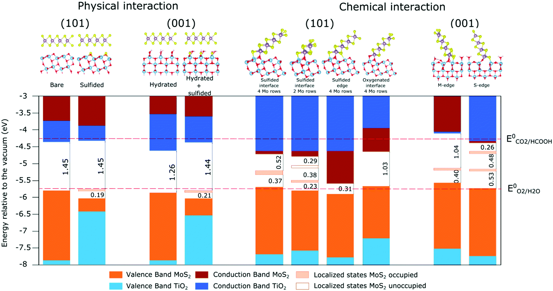 | ||
| Fig. 8 Comparison of the bands positions for all heterojunctions studied in this work: in physical interaction (left panel) and chemical interaction (right panel). | ||
 | ||
| Fig. 9 (a) Possible Z-scheme mechanism for the physical 2D-heterojunction between the MoS2 sheet and the TiO2 (101) surface, (b) Type I heterojunction of the 1D chemical interface between MoS2 nanoribbon (4 Mo rows oxygenated) and the TiO2 (101) surface. Due to the intrinsic semiconductors involved, the Fermi levels are localized in the middle of the bandgap before interaction. | ||
The strong effect of the sulfidation on the electronic structure (diminution of TiO2 bandgap and apparition of a localized state), could favor one of the two mechanisms as a function of the behavior of these localized states. Depending on the mechanism, MoS2 will act as the reducer or as the oxidizer (TiO2 will do the opposite reaction in both cases). This could be an argument in the choice of the mechanism. To do that, tuning by sulfidation the TiO2 surface will be needed through the modification of the pressures of H2S and H2O during a pre-activation step of the material.
Although a clear conclusion about the mechanism that will take place in experiment (“classical” or “Z-scheme”, Fig. 1) is impossible without the knowledge of dynamics of charge carriers, the distribution of charges at the interface and the resulting orientation of the internal electric field before irradiation might help to figure out if the junction will follow a classical or Z-scheme working principle Fig. 9a.14 Hence, the calculation of the Bader charge difference48 between the sub-systems (MoS2 nanosheet and TiO2 surface) before and after junction has been performed (Table 1). In the case of physical interaction, a weak charge transfer occurs from one MoS2 nanosheet to TiO2, which is more significative with the (001) hydrated than with the (101) bare (+0.18 e−vs. +0.02 e− transferred per MoS2 sheet). Obviously, the presence of H-bonding enhances the transfer. Reversely, for both surfaces, the transfer is significantly attenuated by sulfidation of the (001) surface or even inverted for the (101) one (+0.07 e− and −0.04 e−, respectively). As aforementioned, the presence of sulfur-atoms on TiO2 surfaces induces an increase of the distance between the MoS2 sheet and the surface. The fact that the junction involving the TiO2 (001) hydrated surface induces such a negative charge on TiO2 and a positive one on MoS2 could generate the proper internal field with the expected band bending and facilitate a Z-scheme mechanism: the holes generated on MoS2 are attracted by the negatively charged TiO2 and the electrons generated on TiO2 attracted by the positively charged MoS2, which may lead to the targeted electron–hole recombination at the interface upon illumination (Fig. 9a). Moreover, the band gap of the MoS2/(001) TiO2 hydrated heterojunction is 0.2 eV smaller than the one of MoS2/(101) TiO2 which is also a parameter in favor of a Z-scheme mechanism. Hence, the formation of a heterojunction involving the hydrated (001) surface without sulfidation should be sought at the synthesis step. This result might explain in part the recent experimental studies on 2D-2D MoS2/(001) TiO2 nanojunctions30 revealing a H2 evolution rate 36.4 times higher than that of pure TiO2. Our calculations show that the charge transfer increases thanks to a surface contact which could be explained by a Z-scheme mechanism enhancing a spatial separation of the charge carriers while maintaining a good reduction and oxidation power.
| Interaction type | Interfacial structure | Δe− MoS2 (per nanosheet) | Δe− TiO2 |
|---|---|---|---|
| 2D-Physical | (101) bare - infinite sheet | −0.02 | +0.04 |
| (101) sulfided - infinite sheet | +0.04 | −0.09 | |
| (001) hydrated - infinite sheet | −0.18 | +0.36 | |
| (001) hydrated and sulfided - infinite sheet | −0.07 | +0.15 | |
| 1D-Chemical | (101) - Mo-edge (ribbon with 4 Mo rows) | −0.52 | +1.04 |
| (101) - Mo-edge (2 Mo rows) | −0.62 | +1.25 | |
| (101) - Mo-edge sulfided free edge (4 Mo rows) | −0.51 | +1.02 | |
| (001) - oxygenated interface (4 Mo rows) | −0.19 | +0.39 | |
| (001) - Mo-edge (4 Mo rows) | −0.22 | +0.44 | |
| (001) - S-edge (4 Mo rows) | +0.14 | −0.28 |
If we now summarize the band positions of the systems in chemical interaction (Fig. 8), the various MoS2 nanoribbons lead to modifications on the electronic structure of both materials. In fact, while the modification of the number of rows and the modification of the edge leads logically to slight modifications in the band positions, the sulfur/oxygen exchange at the interface implies the modification of the interaction with the TiO2 surface and an increase of its conduction band and valence band. Concerning MoS2, the modification of the number of rows and the sulfidation at the edge narrow the bandgap and eliminate the localized state in the gap. It is accompanied by a shift to the lowest energy in the second case.
In the case of the oxygenated interface, the substitution of the sulfur at the interface has a low impact on MoS2 electronic structure apart the vanishing of the localized states. Concerning the charge transfer analysis (Table 1), we observe once again an electron transfer from MoS2 to TiO2, except in the case with the ribbon in interaction with its S-edge. As expected, the charge transfer is stronger than with the physical interaction (higher than 0.5 electron by nanosheet in the three cases). The strongest charge transfer occurs for the MoS2 nanoribbon of smaller size (2 Mo rows) which may be explained by the strong delocalization of charge within the nanoribbon (Fig. S18, ESI†). Reversely, the charge transfer is limited by the presence of oxygen near the surface (+0.20 for the (101) with oxygenated interface and +0.22 for the ribbon on the (001) hydrated) which is consistent with the large band gap observed for this system. The impact of the electric field induced by this charge transfer on type I heterojunction can be discussed from Fig. 9 b. Due to their respective band positions, these systems could lead to the accumulation of both electrons and holes in the conduction band and valence band of MoS2. In this case, the material should have limited applications as heterojunctions for photocatalysis, particularly in the case of the CO2 photoreduction. In these systems, MoS2 should be considered mainly as a co-catalyst. Nevertheless, due to the induced electric field, the hole transfer facing a barrier could be limited. We cannot rule out the possibility that, due to this barrier, the holes remain on TiO2 which would imply certain potential interest for photocatalytic applications due to good charge separation between TiO2 and MoS2: H2O being oxidized on TiO2 and CO2 being reduced on MoS2 (although the CB level might be slightly insufficient).
Conclusions
Thanks to state of the art DFT calculations including the HSE06 functional, we showed how the various possible structural modifications of the MoS2/TiO2 heterojunction impact the resulting electronic properties: band gaps and CB/VB band positions. In particular, we distinguished the effects of a physical interaction and a chemical one between the MoS2 and TiO2 materials on the nature of the MoS2/TiO2 heterojunctions. A physical 2D-interface may lead to a type II or Z-scheme formalism. The analysis of the CBE/VBE band positions revealed that the physical interaction is compatible with a photocatalytic reduction process of CO2. Moreover, a weak but non-negligible charge transfer occurs from the MoS2 nanosheet to the hydroxylated (001) surface of TiO2 which may induce of a Z-scheme mechanism more efficient for photon absorption processes in photocatalysis applications with reduction of CO2 on MoS2 and oxidation of H2O on TiO2. The sulfidation of the TiO2 surface does not improve the resulting electronic properties. By contrast, all chemical 1D-interfacial systems between MoS2 nanoribbons and TiO2 surfaces imply the formation of a type I heterojunction. The chemical interaction induces a stronger charge transfer at the interface than for the physical interaction but the type I mode will not obligatory enhance the photon absorption efficiency during photocatalysis, except if the barrier for the hole transfer is too high and constrains the hole on TiO2 while electrons are transferred to MoS2.We hope that our theoretical work quantifying the sensitivity of the electronic properties with respect to atomic scale modifications of the MoS2/TiO2 heterostructure will help to provide more rational guides to tune such heterojunction. A perspective of this work would be to evaluate the efficiency of these interfaces to perform the photocatalytic CO2 reduction either by using the Computational Hydrogen Electrode49,50 or even using the Grand Canonical DFT.51
Author contributions
P. R. and T. L. B. designed the research plan. R. F. conducted the DFT calculations and drafted the manuscript. P. R. and T. L. B. supervised the thesis research. All authors participated data analysis and manuscript writing.Conflicts of interest
There are no conflicts to declare.Acknowledgements
This work is part of the “RatiOnAl Design for CATalysis” (ROAD4CAT) industrial chair, project IDEXLYON funded by the French National Research Agency (ANR-16-IDEX-0005) and the Commissariat-General for Investment (CGI) within the framework of Investissements d’Avenir program (“Investment for the future”). The authors thank the SYSPROD project and AXELERA Pôle de Compétitivité for financial support (PSMN Data Center). This work was granted access to the HPC resources of CINES, IDRIS and TGCC under the allocation 2018-080609 made by GENCI.References
- A. Kudo and Y. Miseki, Chem. Soc. Rev., 2009, 38, 253–278 RSC.
- M. G. Walter, E. L. Warren, J. R. McKone, S. W. Boettcher, Q. Mi, E. A. Santori and N. S. Lewis, Chem. Rev., 2010, 110, 6446–6473 CrossRef CAS PubMed.
- X. C. Chen, S. Shen, L. Guo and S. S. Mao, Chem. Rev., 2010, 110, 6503–6570 CrossRef CAS PubMed.
- W. Tu, Y. Zhou and Z. Zou, Adv. Mater., 2014, 26, 4607–4626 CrossRef CAS PubMed.
- X. Chang, T. Wang and J. Gong, Energy Environ. Sci., 2016, 9, 2177 RSC.
- U. Kang, D. S. Han, S. K. Choi, D. J. Ham, S. M. Ji, W. Choi, D. S. Han, A. Abdel-Wahab and H. Park, Energy Environ. Sci., 2015, 8, 2638 RSC.
- U. Ulmer, T. Dingle, P. N. Duchesne, R. H. Morris, A. Tavasoli, T. Wood and G. A. Ozin, Nat. Commun., 2019, 1–12 CAS.
- A. B. Laursen, S. Kegnaes, S. D. Dahl and I. Chorkendorff, Energy Environ. Sci., 2012, 5, 5577 RSC.
- L. Qian, Z. Ning, Y. Yong, W. Guozhong and H. L. N. Dickon, Langmuir, 2014, 30, 8965–8972 CrossRef PubMed.
- M. Shahrokhi, P. Raybaud and T. Le Bahers, ACS Appl. Mater. Interfaces, 2021, 13, 36465–36474 CrossRef CAS PubMed.
- A. R. Beal and H. P. Hughes, J. Phys. C: Solid State Phys., 1979, 12, 881–890 CrossRef CAS.
- K. F. Mak, C. Lee, J. Hone, J. Shan and T. F. Heinz, Phys. Rev. Lett., 2010, 105, 136805 CrossRef PubMed.
- P. Zhou, J. Yu and M. Jaroniec, Adv. Mater., 2014, 26, 4920–4935 CrossRef CAS PubMed.
- X. Li, C. Garlisi, Q. Guan, S. Anwer, K. Al-Ali, G. Palmisano and L. Zheng, Mater. Today, 2021, 47, 75–107 CrossRef CAS.
- B. Chen, Y. Meng, J. Sha, C. Zhong, W. Hu and N. Zhao, Nanoscale, 2018, 10, 34–68 RSC.
- C. Maheu, E. Puzenat, C. Geantet, L. Cardenas and P. Afanasiev, Int. J. Hydrogen Energy, 2019, 44, 18038–18049 CrossRef.
- A. Fujishima, X. Zhanj and D. A. Tryk, Surf. Sci. Rep., 2008, 63, 515–582 CrossRef CAS.
- A. L. Linsebigler, G. Lu and J. T. Yates Jr, Chem. Rev., 1995, 95, 735–758 CrossRef CAS.
- C. G. Morales-Guio, L.-A. Stern and X. Hu, Chem. Soc. Rev., 2014, 43, 6555–6569 RSC.
- R. Arancon, M. Saab, A. Morvan, A. Bonduelle-Skrzypczak, A.-L. Taleb, A.-S. Gay, C. Legens, O. Ersen, K. Searles, V. Mougel, A. Fedorov, C. Copéret and P. Raybaud, J. Phys. Chem. C, 2019, 123, 24659–24669 CrossRef CAS.
- W. Zhang, X. Xiao, Y. Li, X. Zheng, L. Zheng and C. Whan, RSC Adv., 2016, 6, 33705–33712 RSC.
- X. Liu, Z. Xing, H. Zhang, W. Wang, Y. Zhang, Z. Li, X. Wu, X. Yu and W. Zhou, ChemSusChem, 2016, 9, 1118–1124 CrossRef CAS PubMed.
- W. Tu, Y. Li, L. Kuai, Y. Zhou, Q. Xu, H. Li, X. Wang, M. Xiao and Z. Zou, Nanoscale, 2017, 9, 9065–9070 RSC.
- S. Kanda, T. Akita, M. Fujishima and H. Tada, J. Colloid Interface Sci., 2011, 354, 607–610 CrossRef CAS PubMed.
- M. Shen, Z. Yan, L. Yang, P. Du, J. Zhang and B. Xiang, Chem. Commun., 2014, 50, 15447–15449 RSC.
- W. Zhou, Z. Yin, Y. Du, X. Huang, Z. Zeng, Z. Fan, H. Liu, J. Wang and H. Zhang, Small, 2013, 9, 140–147 CrossRef CAS PubMed.
- X. Zhou, M. Licklederer and P. Schmuki, Electrochem. Commun., 2016, 73, 33–37 CrossRef CAS.
- M. Lazzeri, A. Vittadini and A. Selloni, Phys. Rev. B: Condens. Matter Mater. Phys., 2001, 63, 155409 CrossRef.
- C. Arrouvel, M. Digne, M. Breysse, H. Toulhoat and P. Raybaud, J. Catal., 2004, 222, 152–166 CrossRef CAS.
- Y.-J. Yuan, Z.-J. Ye, H. Lu, B. Hu, Y.-H. Li, D. Chen, J.-S. Zhong, Z.-T. Yu and Z. Zou, ACS Catal., 2016, 6, 532–541 CrossRef CAS.
- C. Arrouvel, M. Breysse, H. Toulhoat and P. Raybaud, J. Catal., 2005, 232, 161–178 CrossRef CAS.
- D. Costa, C. Arrouvel, M. Breysse, H. Toulhoat and P. Raybaud, J. Catal., 2007, 246, 325–343 CrossRef CAS.
- Y. Sakashita, Y. Araki, K. Honna and H. Shimada, Appl. Catal., A, 2000, 197, 247–253 CrossRef CAS.
- G. Kresse and J. Furthmüller, Comput. Mater. Sci., 1996, 6, 15–50 CrossRef CAS.
- G. Kresse and J. Furthmüller, Phys. Rev. B: Condens. Matter Mater. Phys., 1996, 54, 11169–11186 CrossRef CAS PubMed.
- J. P. Perdew, K. Burke and M. Ernzerhof, Phys. Rev. Lett., 1996, 77, 3865–3868 CrossRef CAS PubMed.
- J. Heyd and G. E. Scuseria, J. Chem. Phys., 2004, 121, 1187–1192 CrossRef CAS PubMed.
- S. Grimme, S. Ehrlich and L. Goerigk, J. Comput. Chem., 2011, 32, 1456–1465 CrossRef CAS PubMed.
- K. Mattew, R. Sundararaman, K. Letchworth-Weaver, T. A. Arias and R. G. Hennig, J. Chem. Phys., 2014, 140, 084106 CrossRef PubMed.
- J. Kullgren, B. Aradi, T. Frauenheim, L. Kavan and P. Deak, J. Phys. Chem. C, 2015, 119, 21952–21958 CrossRef CAS.
- H. Han, K. M. Kim, C.-W. Lee, C. S. Lee, R. C. Pawar, J. L. Jones, Y.-R. Hong, J. H. Ryu, T. Song, S. H. Kang, H. Choi and S. Mhin, Phys. Chem. Chem. Phys., 2017, 19, 28207–28215 RSC.
- C. Arrouvel, H. Toulhoat, M. Breysse and P. Raybaud, J. Catal., 2004, 226, 260–272 CrossRef CAS.
- L. Coulier, J. van Veen and J. Niemantsverdriet, Catal. Lett., 2002, 79, 149–155 CrossRef CAS.
- H. Schweiger, P. Raybaud, G. Kresse and H. Toulhoat, J. Catal., 2002, 207, 76–87 CrossRef CAS.
- P. Raybaud, J. Hafner, G. Kresse, S. Kasztelan and H. Toulhoat, J. Catal., 2000, 189, 129–146 CrossRef CAS.
- R. G. Leliveld, A. J. van Dillen, J. W. Geus and D. C. Koningsberger, J. Catal., 1997, 165, 184–196 CrossRef CAS.
- B. Baubet, A.-S. Gay, A.-L. Taleb, M. Moreaud, F. Wahl, V. Delattre, E. Devers, A. Hugon, O. Ersen, P. Afanasiev and P. Raybaud, ACS Catal., 2016, 6, 1081–1092 CrossRef CAS.
- R. F. W. Bader, Atoms in Molecules – A Quantum Theory, Oxford university press, New York, 1990 Search PubMed.
- M. Bajdich, M. Garcia-Mota, A. Vojvodic, J. K. Nørskov and A. T. Bell, J. Am. Chem. Soc., 2013, 135, 13521–13530 CrossRef CAS PubMed.
- L. Lv, Y. Shen, X. Gao, J. Liu, S. Wu, Y. Ma, X. Wang, D. Gong and Z. Zhou, Appl. Surf. Sci., 2021, 546, 149066 CrossRef CAS.
- A. Curutchet, P. Colinet, C. Michel, S. N. Steinmann and T. Le Bahers, Phys. Chem. Chem. Phys., 2020, 22, 7031–7038 RSC.
Footnote |
| † Electronic supplementary information (ESI) available. See DOI: 10.1039/d1cp05151b |
| This journal is © the Owner Societies 2022 |