
 Open Access Article
 This Open Access Article is licensed under a
 Creative Commons Attribution 3.0 Unported Licence
Surface and interface effects in oxygen-deficient SrMnO3 thin films grown on SrTiO3†
Moloud
Kaviani
and
Ulrich
Aschauer
 *
*
Department of Chemistry, Biochemistry and Pharmaceutical Sciences, University of Bern, Freiestrasse 3, CH-3012 Bern, Switzerland. E-mail: ulrich.aschauer@unibe.ch
First published on 31st January 2022
Abstract
Complex oxide functionality, such as ferroelectricity, magnetism or superconductivity is often achieved in epitaxial thin-film geometries. Oxygen vacancies tend to be the dominant type of defect in these materials but a fundamental understanding of their stability and electronic structure has so far mostly been established in the bulk or strained bulk, neglecting interfaces and surfaces present in a thin-film geometry. We investigate here, via density functional theory calculations, oxygen vacancies in the model system of a SrMnO3 (SMO) thin film grown on a SrTiO3 (STO) (001) substrate. Structural and electronic differences compared to bulk SMO result mainly from undercoordination at the film surface. The changed crystal field leads to a depletion of subsurface valence-band states and transfer of this charge to surface Mn atoms, both of which strongly affect the defect chemistry in the film. The result is a strong preference of oxygen vacancies in the surface region compared to deeper layers. Finally, for metastable oxygen vacancies in the substrate, we predict a spatial separation of the defect from its excess charge, the latter being accommodated in the film but close to the substrate boundary. These results show that surface and interface effects lead to significant differences in stability and electronic structure of oxygen vacancies in thin-film geometries compared to the (strained) bulk.
1 Introduction
Transition-metal perovskite oxides represent an extremely versatile class of materials that can host a large range of functional properties such as ferroelectricity, magnetism or superconductivity.1,2 The emergence of these properties can often be tuned by bi-axial strain, imposed for example by lattice matching during coherent epitaxial growth on a substrate with different lattice parameter.3 Compared to bulk perovskite oxides, fundamental changes in properties occur in these thin films. Ferroelectricity and magnetism can, for example, be enhanced4 or even introduced in the thin-film material.5,6 Moreover, interfaces between the substrate and the film or between different layers of a heterostructure have emerged as an avenue to generate rich and novel electronic phases.3Depending on the synthesis conditions, complex oxides typically contain point defects that can strongly affect conductive, ferroelectric or magnetic properties useful for applications in electronics. While often detrimental to functional properties, defects were also shown to induce novel functionalities in specific cases.7,8 Oxygen vacancies (VO) are particularly abundant in perovskite oxides under typical synthesis conditions. Depending on their charge state and the localization of the excess charge, VO may lead to changes in oxidation state and local distortions that affect the ferroelectric and magnetic properties.9–11 Point-defect engineering could thus be a route to tailor properties for a given application. Our understanding of point defects and their formation energetics and electronic structure is, however, currently mostly limited to idealized bulk or strained bulk systems, neglecting the effect of the substrate–film interface and the film surface, except for select cases like the LAO/STO interface.12 Therefore, realistic models containing both surfaces and hetero-interface with the substrate are crucially needed to accurately assess defect-induced phenomena in thin-film systems.
In the present work, we use the model system of a SrMnO3 (SMO) thin film grown on a typical (001) TiO2-terminated SrTiO3 (STO) substrate to study the formation and electronic structure of VO in a thin-film geometry. This model system has recently been experimentally realized, showing excess charge accommodation in the film but close to the interface.13 The thermodynamic ground state of SMO is a hexagonal phase,14 but it is synthesizable in an orthorhombic perovskite structure when grown on a perovskite structured substrate,8,15,16 possibly adopting ordered Brownmillerite phases at high oxygen deficiency.17 SMO adopts a G-type antiferromagnetic order with Mn atoms of alternating spin arranged in a 3D checkerboard pattern. Alternatively, this magnetic order can be seen as alternating spins on adjacent Mn-containing (111) planes. VO were previously studied in both materials separately. In SMO and related manganites such as CaMnO3 and BaMnO3, the three 3d electrons in Mn4+ fully occupy the t2g orbitals of majority-spin in the G-type AFM order. Upon VO creation, the eg orbitals of Mn adjacent to the defect are stabilized and accommodate the two excess electrons, resulting in a reduction of both Mn from Mn4+ to Mn3+.8,18,19 This is energetically much preferred over the reduction of a single Mn to Mn2+. We note that the oxygen vacancy in this setup is doubly positively charged with respect to the O2− lattice site and charge compensated by the reduction of the two adjacent Mn4+ to Mn3+. It was also shown that magnetic order and polar distortions can affect the formation energy of VO in these materials.19,20 In STO, a large variability in the experimental and theoretical literature reveals that states with excess charge accommodation in the t2g conduction band or in shallow eg defect states are close in energy, results depending also on the crystal structure (cubic or tetragonal) and the size of the simulation cell.21 For electrons in the t2g conduction band, the vacancy is doubly positively charged with respect to the O2− lattice site and charge compensated by free electrons, while the vacancy with electrons in eg defect states forms an F-center with the same charge as the O2− lattice site. We note that for SMO, on the other hand, charge localization around an oxygen vacancy does not significantly depend on the cell size and that oxygen-vacancy formation energies computed for one vacancy per 8 formula-unit, 40 atom cell in the related CaMnO318 agree well with those observed in experiment.22
For the thin-film geometry, our DFT+U calculations show that crystal-field changes of the under-coordinated surface atoms lead to a charge transfer towards the surface and hence surface Mn3+ species. This asymmetric structure leads to an electric field in this nominally non-polar interface, which strongly affects the defect chemistry. We find that vacancies more easily form at the surface and that the formation energy increases in a near linear fashion with increasing distance from the surface. For oxygen vacancies in the STO substrate, we predict separation of the defect and the charge, the latter residing on Mn atoms at the interface, which leads to a marked reduction in formation energy compared to bulk STO. For our model system, the formation of oxygen vacancies is, therefore, greatly different compared to either of the bulk materials.
2 Methods
DFT calculations were performed using Quantum ESPRESSO23,24 at the PBE+U level of theory25,26 with Hubbard U calculated self-consistently27–29 as 4.26 and 4.48 eV for the Mn and Ti 3d orbitals respectively.20,21 All atoms are represented by ultrasoft pseudopotentials30 with Sr(4s, 4p, 5s), Mn(3p, 4s, 3d), O(2s, 2p) and Ti(3s, 3p, 3d, 4s) valence electrons. The cutoff for the plane-wave basis was 70 Ry for the kinetic energy combined with 840 Ry for the augmented density.We model a SMO thin film, grown epitaxially on a (001) STO substrate. Unstrained perovskite SMO has a paraelectric Pnma structure with a G-type antiferromagnetic order,31 which we use to initialize all calculations throughout this work. The structure is close to the ideal cubic structure with small octahedral tilts and rotations found computationally but not yet observed experimentally.32 The STO substrate undergoes, around 105 K,33,34 a transition from a high-temperature cubic (space group Pm![[3 with combining macron]](https://www.rsc.org/images/entities/char_0033_0304.gif) m) to a tetragonal antiferrodistortive (AFD, space group I4/mcm) phase, where TiO6 octahedra rotate around the c-axis with out-of-phase rotations in consecutive layers (a0a0c− in Glazer notation35). Since our DFT calculations are performed at 0 K, we use the relevant AFD phase of STO.
m) to a tetragonal antiferrodistortive (AFD, space group I4/mcm) phase, where TiO6 octahedra rotate around the c-axis with out-of-phase rotations in consecutive layers (a0a0c− in Glazer notation35). Since our DFT calculations are performed at 0 K, we use the relevant AFD phase of STO.
We construct the STO substrate from the fully relaxed AFD structure as a TiO2 terminated 80-atom supercell slab that has 2 × 2 × 4 dimensions compared to the 5-atom cubic cell. The Pnma SMO film also has 2 × 2 × 4 dimensions compared to the 5-atom cubic cell and is MnO2 terminated. We note that one VO per 160-atom supercell results in a defect concentrations slightly smaller than observed in typical experiments of manganite films.18,22 Larger lateral dimensions of the simulation cell lead to negligible changes in formation energies and electronic structure (see Section S4, ESI†). Due to lattice mismatch between STO and SMO, the SMO film experiences tensile strain of about 1.5% when its lattice parameters are adjusted to match the STO substrate. We separate periodic images along the film normal by a 12 Å vacuum and employ a dipole correction in this vacuum layer.36 The lowest two atomic layers of the substrate are fixed at bulk positions to mimic the presence of a large and rigid bulk.
The Brillouin zone of this thin-film system is sampled using a 6 × 6 × 1 Monkhorst–Pack37k-point grid. The convergence criteria for geometry relaxations were 5 × 10⁻³ eV Å−1 for forces and 10−5 eV for the total energy. Oxygen vacancies can, in principle, occur in multiple charge states when electrons are removed from the cell in addition to the oxygen atom. As shown in Fig. S4 (ESI†), under conditions relevant for materials such as SMO, the charge state without removed electrons dominates. Moreover this charge state is most relevant for oxides that do not contain additional donor or acceptor species that could charge balance ionized oxygen vacancies. The formation energy Ef,VO of an oxygen vacancy (VO) was calculated as described in ref. 38:
| Ef,VO = Etot,VO − Etot,stoi + μO, | (1) |
3 Results and discussion
3.1 Stoichiometric thin film
Our thin-film model deviates from SMO bulk in a number of ways that are expected to also affect the behavior and properties of defective films. Due to tensile strain the in-plane (IP) dimensions of SMO are expanded, while the out-of-plane (OP) dimension shrinks according to Poisson's ratio.40 This change in lattice parameters is accommodated by changes in Mn–O bond lengths and Mn–O–Mn bond angles (see Fig. 1a and d). In particular the IP Mn–O–Mn angles straighten out at the surface and approach 180°, while the OP bond-angles remain close to the bulk value. We note however that the OP bond-angles are strongly affected at the interface to match the a0a0c− STO rotation pattern. The c/a ratio of the film is 0.98, in line with the slight tensile strain.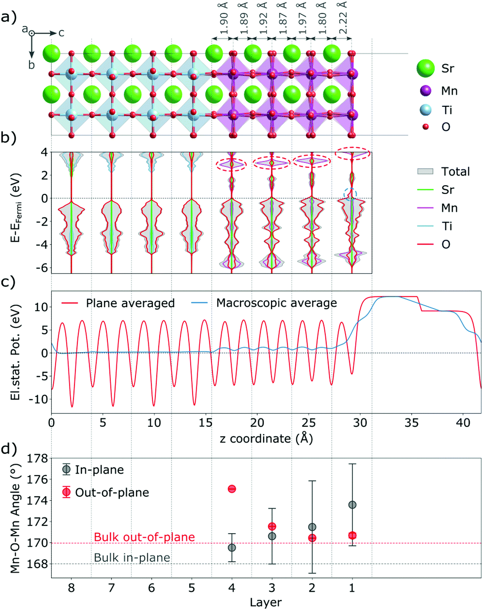 | ||
| Fig. 1 Stoichiometric SMO thin film on a STO substrate: (a) structure and selected interplanar spacings, (b) total and projected layer-resolved density of states (dashed ovals mark features discussed in the text), (c) electrostatic potential and (d) Mn–O–Mn bond angles. | ||
The truncation of Mn–O bonds at the film surface changes the crystal field of surface Mn atoms from octahedral to approximately square pyramidal. Changes in crystal field were previously shown to affect defect stability in the bulk41–43 as well as at surfaces,44 while their effect in a thin film geometry was not yet analyzed. The concomitant lowering of Mn 3d energies leads to more favorable electron accommodation at the surface compared to Mn sites in other layers. This change is visible in the layer-resolved projected density of states (Fig. 1b, where at the very surface the characteristic t2g peak visible around 3 eV in lower MnO2 layers (circled in red) is significantly destabilized and a small minority-spin (down-polarized Mn) peak is visible just above the Fermi energy (circled in blue). This change in the electronic structure leads to a ferrimagnetic surface layer (see Fig. 1b as well as Fig. S1, ESI† for a narrower energy range around the Fermi level and Fig. S2, ESI† for a comparison of the density of states at deeper layers of the thin film and substrate with bulk SrMnO3 and SrTiO3).
We evaluated the oxidation state of these surface atoms according to the method proposed in ref. 45, based on the Mn 3d-electron occupation matrix, and found it to be Mn3+, while Mn atoms in all other layers retain their nominal Mn4+ oxidation state. We verified that the change in oxidation state is not an artefact of the geometry. As shown in Fig. S3 (ESI†), we observe the same change in electronic structure in asymmetric and symmetric SMO surface slabs, indicating that it is an intrinsic feature of MnO2-terminated SMO surfaces and not caused by the asymmetry of the setup. Based on the projected layer-resolved densities of states (see Fig. 1b) the electrons leading to surface Mn3+ stem from lower lying SMO layers that are slightly electron depleted.
This charge transfer towards the surface has two effects. On one hand, the reduction from Mn4+ to Mn3+ at the surface causes an increase in ionic radius, which manifests in an expansion of the SrO–MnO2 interlayer spacing by about 0.3 Å from 1.91 Å in the bulk to 2.20 Å at the surface, as visible in Fig. 1a). This structural distortion propagates into lower layers, where we observe shorter interlayer spacings below SrO layers (from 1.91 Å to 1.80 Å below the first SrO layer), while those below MnO2 layers are expanded. Such a change in geometry will affect the crystal field and could alter the excess charge accommodation upon oxygen vacancy formation. On the other hand, the presence of Mn3+ at the surface will repel electrons from the surface. As shown in Fig. 1(c), the change in electrostatic potential is greatest at the surface but a small field exists throughout the whole film. This electric field will lead to excess charges being more favorably accommodated further away from the surface. Nevertheless we note that the SMO film has empty states at lower energies than the STO substrate, which is expected to keep excess-charges in the film rather than the substrate. In the next section, we will investigate how the aforementioned changes in the ionic and electronic structure affect the formation of oxygen vacancies in the thin-film.
3.2 Oxygen vacancies in the thin film
In Fig. 2 we show the formation energy of oxygen vacancies (VO) in the different layers of the thin film. Within each layer, multiple symmetry inequivalent VO positions exist, the variation in formation energy of which is however negligible compared to the effect of the distance from the surface. We observe an increasing trend (by more than 1 eV) in formation energy from the surface to the hetero-interface, which continues into the substrate. This implies that VO will have a tendency to be formed in the surface region, respectively to migrate there, if oxygen mobility is sufficiently high. As indicated by horizontal dashed lines in Fig. 2, it is noteworthy that oxygen vacancy formation in the ultra-thin film is always more favorable than in the bulk, only the SrO layer at the interface reaching the VO formation energy of bulk SMO. The VO formation energy in the substrate, on the other hand, is always lower than in bulk STO. This hints at a different electronic structure of the VO compared to the bulk phases.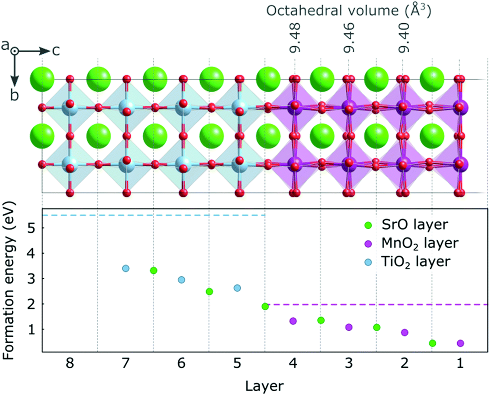 | ||
| Fig. 2 Formation energy for VO under O rich conditions in different layers of the SMO film and the STO substrate. The dashed horizontal lines indicate the theoretical values of the formation energies in 40-atom SMO and STO bulk cells. MnO6 octahedral volumes are indicated above the structure. | ||
The metallic nature of the stoichiometric surface layer greatly complicates the analysis of the electronic structure in presence of a VO and we hence start our discussion with vacancies in the SrO layers, returning to MnO2 layers below. In bulk manganites, VO formation results in a lowering of the eg states of the two Mn atoms adjacent to the vacancy, which become the lowest unoccupied states and accommodate the excess electrons resulting from VO formation.8,18,20 In the topmost SrO layer of our thin film, we observe a different picture. Instead of localizing on one Mn atom each in the surface and first subsurface MnO2 layers, we observe the typical Mn eg defect state only in the first subsurface layer (circled in Fig. 3a). We note that this state remains unoccupied, while we observe filling of the valence-band states, notably in the second layer, that were empty due to the crystal-field changes at the stoichiometric surface. This implies that the charge primarily localizes in the layer below the vacancy, however not in the typical Mn eg defect states.
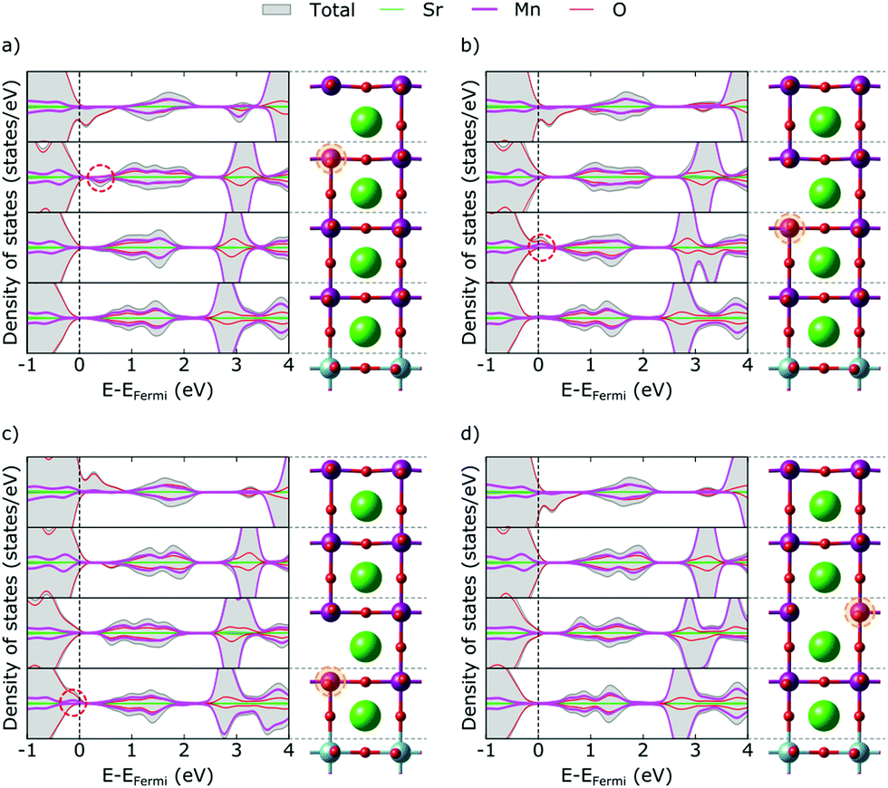 | ||
| Fig. 3 Total and projected layer-resolved density of states for VO (a) in the first, (b) second and (c) third SrO layer and (d) in the third MnO2 layer. Dashed ovals mark features discussed in the text. The primarily reduced Mn sites are circled in orange. | ||
We see the same pattern also in the second and third SrO layer (Fig. 3b and c), but note that with increasing depth the circled Mn eg defect state becomes occupied while the valence-band states in the first subsurface layer are again empty. We associate this with the slight upwards band bending at the surface induced by the Mn3+ ions that causes the defect state in layers further from the surface to be lower in energy than closer to the surface. This is also in agreement with the fact that electrons always localize in layers below the defect, i.e. further away from the surface. Moreover, the reduction-less excess-charge accommodation in valence-band states explains the lower formation energy close to the surface, which gradually increases due to increased defect-state occupation in layers further from the surface.
The only exception to this excess-charge accommodation pattern occurs in the SrO layer at the SMO–STO interface, where the VO is formed between a Mn and a Ti atom. Here the reduction occurs on the Mn above the VO, which can be rationalized by the lower lying empty Mn states compared to the empty Ti states (see Fig. 1b). This change in electronic structure can account for the marked increase in formation energy for this layer, compared to layers closer to the surface (see Fig. 2).
For VO in the MnO2 layers (exemplified for the third MnO2 layer in Fig. 3d) we observe an asymmetry of eg peaks in the majority and minority spin channels. Indeed, we observe significantly more Mn eg density of states in the valence band of the vacancy layer than for the other layers. We thus conclude that one of the two Mn sites next to the VO gets reduced (the spin-down Mn in the G-AFM order in this case), whereas the other (the spin-up Mn) does not get reduced, the remaining electron filling the empty valence-band states.
The variation in bond lengths discussed for the stoichiometric surface leads to changes in the octahedral volumes and one could, via chemical expansion arguments,18,46 expect the VO formation energy to be inversely correlated with the polyhedral volume in the stoichiometric structure. While the strongly expanded truncated polyhedron at the surface is indeed associated with a low formation energy, this trend does not continue towards the interface (see octahedral volumes Fig. 2) since the octahedral volumes increase as does the formation energy. We therefore believe the VO formation energy to be dominated by the band bending induced by the reduced surface Mn3+ ions.
3.3 Oxygen vacancies in the substrate
In bulk STO, the two excess electrons associated with a VO localize in F-center like states derived from Ti eg orbitals and possibly also populate the conduction band if a spin triplet state is allowed.9,21,47–49 In our thin film setup we observe, on the contrary, no localization of electrons in the vicinity of a VO created in the STO substrate. On the contrary both for a VO created in a TiO2 or in a SrO layer of the substrate, the excess electrons primarily localize on Mn states at the bottom of the SMO thin film but also fill the above-mentioned valence-band states induced by surface Mn3+ (see Fig. 4). | ||
| Fig. 4 Total and projected layer-resolved density of states for VO (a) in the first TiO2 layer and (b) in the first SrO layer of the STO substrate. Dashed ovals mark features discussed in the text. The primarily reduced Mn sites are circled in orange. | ||
This separation of the VO defect from it's excess charge occurs – at least within the scale of our computational model – independently of the distance of the VO from the interface and can be rationalized by the significant energy difference between empty Mn and Ti states (see Fig. 1). The defect formation energy can be significantly lowered by accommodating electrons in energetically more favorable Mn states than in Ti states that are either in the STO conduction band or just below the conduction band edge.
This interfacial charge transfer is the reason behind the reduced formation energy compared to bulk STO.21 Nevertheless we note that VO formation energies will always be significantly larger in the substrate compared to the thin film and that VO will have a driving force for migration from the STO substrate into the SMO thin film.
4 Conclusions
In this work, we investigated the effect of the surface and hetero-interface on oxygen vacancies in SrMnO3 thin films grown on a SrTiO3 substrate. We show that the altered crystal field at a MnO2 terminated film surface leads to a charge transfer from valence-band states in lower layers to the surface, forming reduced Mn3+ ions at the very surface. This alteration affects oxygen-vacancy formation in the film in two ways. On one hand the holes created in the film due to the above-mentioned charge transfer accommodate some of the excess charge induced by oxygen vacancies. On the other hand, the remaining excess charge that localizes in the vicinity of the vacancy is affected by the surface-Mn3+ induced band bending, which leads to formation energies that gradually increase from the surface to the interface. We further show that vacancies in the SrTiO3 substrate have larger formation energies compared to the SrMnO3 film but transfer electrons to the film, which lowers their formation energy compared to bulk SrTiO3.A previous experimental study13 on the same thin film system, used EELS to detect an increased electron density in the MnO2 layer closest to the substrate. This was explained based on multiple origins, among them oxygen vacancy formation in the film and a reduction of the substrate under deposition conditions. Based on our findings, oxygen vacancies in the SrMnO3 film would have to reside at the very interface to induce charges in that layer. Since there is no driving force for vacancy accumulation close to the interface and since vacancies in other layers would also affect the Mn oxidation state in these layers, oxygen vacancies in SrMnO3 seem an unlikely source for the experimental observations. On the other hand, oxygen vacancies in the substrate (likely to be formed under vacuum deposition conditions) would consistently lead to charges in the layer observed by experiment and are a more likely scenario.
Our results show that oxygen vacancy formation in a thin-film geometry can be significantly different from a bulk or strained bulk situation. Not only can the film surface induce subtle changes in the electronic structure that affect excess charge accommodation and stability of oxygen vacancies, but the film can also attract excess electrons from the substrate. These effects are not captured in established strained bulk calculations and are expected to strongly depend on the properties of the film and the substrate. In the present SrMnO3 film grown on top of a SrTiO3 substrate, these effects lead to a metallic and ferrimagnetic surface with potential applications, in particular, in oxide electronics. We expect similar behavior in other perovskite oxide films with multivalent B-site cations, but note that the different d-orbital occupation can strongly alter the crystal-field effects. Detailed studies on other film materials will be a worthy topic for future studies but we stress that gaining a fundamental understanding of defects in oxide thin films will have to involve surface and interface effects in addition to strain effects.
Data availability
The main Quantum ESPRESSO pw.x input and output files needed to compute the formation energies in Fig. 2 are available on the Materials Cloud Archive at DOI: http://10.24435/materialscloud:1y-q7.Conflicts of interest
There are no conflicts to declare.Acknowledgements
This work was supported by the Swiss National Science Foundation under Project 200021_178791. Calculations were performed on UBELIX (http://www.id.unibe.ch/hpc), the HPC cluster at the University of Bern and on Piz Daint at the Swiss Supercomputing Center CSCS under projects s955 and s1033.Notes and references
- X. Lin, Z. Zhu, B. Fauqué and K. Behnia, Phys. Rev. X, 2013, 3, 021002 CAS
.
- S. Saremi, R. Xu, F. I. Allen, J. Maher, J. C. Agar, R. Gao, P. Hosemann and L. W. Martin, Phys. Rev. Mater., 2018, 2, 084414 CrossRef CAS
- J. Mannhart and D. G. Schlom, Science, 2010, 327, 1607–1611 CrossRef CAS
- J. Wang, J. B. Neaton, H. Zheng, V. Nagarajan, S. B. Ogale, B. Liu, D. Viehland, V. Vaithyanathan, D. G. Schlom, U. V. Waghmare, N. A. Spaldin, K. M. Rabe, M. Wuttig and R. Ramesh, Science, 2003, 299, 1719–1722 CrossRef CAS PubMed
- W. S. Choi, J.-H. Kwon, H. Jeen, J. E. Hamann-Borrero, A. Radi, S. Macke, R. Sutarto, F. He, G. A. Sawatzky, V. Hinkov, M. Kim and H. N. Lee, Nano Lett., 2012, 12, 4966–4970 CrossRef CAS PubMed
- D. Fuchs, C. Pinta, T. Schwarz, P. Schweiss, P. Nagel, S. Schuppler, R. Schneider, M. Merz, G. Roth and H. V. Löhneysen, Phys. Rev. B: Condens. Matter Mater. Phys., 2007, 75, 144402 CrossRef
- V. Sharma, A. Herklotz, T. Z. Ward and F. A. Reboredo, Sci. Rep., 2017, 7, 11166 CrossRef
- C. Becher, L. Maurel, U. Aschauer, M. Lilienblum, C. Magén, D. Meier, E. Langenberg, M. Trassin, J. Blasco, I. P. Krug, P. A. Algarabel, N. A. Spaldin, J. Pardo and M. Fiebig, Nat. Nanotechnol., 2015, 10, 661–665 CrossRef CAS PubMed
- M. Choi, F. Oba, Y. Kumagai and I. Tanaka, Adv. Mater., 2013, 25, 86–90 CrossRef CAS
- J. B. Goodenough, Rep. Prog. Phys., 2004, 67, 1915–1993 CrossRef CAS
- H. Taguchi, M. Shimada and M. Koizumi, J. Solid State Chem., 1979, 29, 221–225 CrossRef CAS
- L. Yu and A. Zunger, Nat. Commun., 2014, 5, 5118 CrossRef CAS
- H. Wang, V. Srot, X. Jiang, M. Yi, Y. Wang, H. Boschker, R. Merkle, R. W. Stark, J. Mannhart and P. A. van Aken, ACS Nano, 2020, 14, 12697–12707 CrossRef PubMed
- T. Negas and R. S. Roth, J. Solid State Chem., 1970, 1, 409–418 CrossRef
- A. Daoud-Aladine, C. Martin, L. C. Chapon, M. Hervieu, K. S. Knight, M. Brunelli and P. G. Radaelli, Phys. Rev. B: Condens. Matter Mater. Phys., 2007, 75, 104417 CrossRef
- L. Maurel, N. Marcano, T. Prokscha, E. Langenberg, J. Blasco, R. Guzmán, A. Suter, C. Magén, L. Morellón, M. R. Ibarra, J. A. Pardo and P. A. Algarabel, Phys. Rev. B: Condens. Matter Mater. Phys., 2015, 92, 024419 CrossRef
- S. Kobayashi, Y. Ikuhara and T. Yamamoto, Appl. Phys. Lett., 2013, 102, 231911 CrossRef
- U. Aschauer, R. Pfenninger, S. M. Selbach, T. Grande and N. A. Spaldin, Phys. Rev. B: Condens. Matter Mater. Phys., 2013, 88, 054111 CrossRef
- A. Marthinsen, C. Faber, U. Aschauer, N. A. Spaldin and S. M. Selbach, MRS Commun., 2016, 6, 182–191 CrossRef CAS
- C. Ricca, I. Timrov, M. Cococcioni, N. Marzari and U. Aschauer, Phys. Rev. B, 2019, 99, 094102 CrossRef
- C. Ricca, I. Timrov, M. Cococcioni, N. Marzari and U. Aschauer, Phys. Rev. Res., 2020, 2, 023313 CrossRef CAS
- L. Rørmark, A. B. Mørch, K. Wiik, S. Stølen and T. Grande, Chem. Mater., 2001, 13, 4005–4013 CrossRef
- P. Giannozzi, S. Baroni, N. Bonini, M. Calandra, R. Car, C. Cavazzoni, D. Ceresoli, G. L. Chiarotti, M. Cococcioni, I. Dabo, A. D. Corso, S. de Gironcoli, S. Fabris, G. Fratesi, R. Gebauer, U. Gerstmann, C. Gougoussis, A. Kokalj, M. Lazzeri, L. Martin-Samos, N. Marzari, F. Mauri, R. Mazzarello, S. Paolini, A. Pasquarello, L. Paulatto, C. Sbraccia, S. Scandolo, G. Sclauzero, A. P. Seitsonen, A. Smogunov, P. Umari and R. M. Wentzcovitch, J. Phys.: Condens. Matter, 2009, 21, 395502 CrossRef
- P. Giannozzi, O. Andreussi, T. Brumme, O. Bunau, M. B. Nardelli, M. Calandra, R. Car, C. Cavazzoni, D. Ceresoli, M. Cococcioni, N. Colonna, I. Carnimeo, A. D. Corso, S. de Gironcoli, P. Delugas, R. A. J. DiStasio, A. Ferretti, A. Floris, G. Fratesi, G. Fugallo, R. Gebauer, U. Gerstmann, F. Giustino, T. Gorni, J. Jia, M. Kawamura, H.-Y. Ko, A. Kokalj, E. Kucukbenli, M. Lazzeri, M. Marsili, N. Marzari, F. Mauri, N. L. Nguyen, H.-V. Nguyen, A. Otero-de-la Roza, L. Paulatto, S. Poncé, D. Rocca, R. Sabatini, B. Santra, M. Schlipf, A. P. Seitsonen, A. Smogunov, I. Timrov, T. Thonhauser, P. Umari, N. Vast, X. Wu and S. Baroni, J. Phys.: Condens. Matter, 2017, 29, 465901 CrossRef CAS
- J. P. Perdew, K. Burke and M. Ernzerhof, Phys. Rev. Lett., 1996, 77, 3865–3868 CrossRef CAS PubMed
- V. I. Anisimov, J. Zaanen and O. K. Andersen, Phys. Rev. B: Condens. Matter Mater. Phys., 1991, 44, 943–954 CrossRef CAS PubMed
- M. Cococcioni and S. de Gironcoli, Phys. Rev. B: Condens. Matter Mater. Phys., 2005, 71, 035105 CrossRef
- H. Hsu, K. Umemoto, M. Cococcioni and R. Wentzcovitch, Phys. Rev. B: Condens. Matter Mater. Phys., 2009, 79, 125124 CrossRef
- I. Timrov, N. Marzari and M. Cococcioni, Phys. Rev. B, 2018, 98, 085127 CrossRef
- D. Vanderbilt, Phys. Rev. B: Condens. Matter
Mater. Phys., 1990, 41, 7892–7895 CrossRef
- O. Chmaissem, B. Dabrowski, S. Kolesnik, J. Mais, D. E. Brown, R. Kruk, P. Prior, B. Pyles and J. D. Jorgensen, Phys. Rev. B: Condens. Matter Mater. Phys., 2001, 64, 134412 CrossRef
- J. H. Lee and K. M. Rabe, Phys. Rev. Lett., 2010, 104, 207204 CrossRef PubMed
- R. A. Cowley, W. J. L. Buyers and G. Dolling, Solid State Commun., 1969, 7, 181–184 CrossRef CAS
- G. Shirane and Y. Yamada, Phys. Rev., 1969, 177, 858–863 CrossRef CAS
- A. M. Glazer, Acta Crystallogr., Sect. B, 1972, 28, 3384–3392 CrossRef CAS
- L. Bengtsson, Phys. Rev. B: Condens. Matter Mater. Phys., 1999, 59, 12301–12304 CrossRef CAS
- H. J. Monkhorst and J. D. Pack, Phys. Rev. B: Solid State, 1976, 13, 5188–5192 CrossRef
- C. Freysoldt, B. Grabowski, T. Hickel, J. Neugebauer, G. Kresse, A. Janotti and C. G. Van de Walle, Rev. Mod. Phys., 2014, 86, 253–305 CrossRef
- L. Wang, T. Maxisch and G. Ceder, Phys. Rev. B: Condens. Matter Mater. Phys., 2006, 73, 195107 CrossRef
- P. Agrawal, J. Guo, P. Yu, C. Hébert, D. Passerone, R. Erni and M. D. Rossell, Phys. Rev. B, 2016, 94, 104101 CrossRef
- X. Jia, W. Yang, M. Qin and J. Li, J. Magn. Magn. Mater., 2009, 321, 2354–2358 CrossRef CAS
- F. El-Mellouhi, E. N. Brothers, M. J. Lucero and G. E. Scuseria, J. Phys.: Condens. Matter, 2013, 25, 135501 CrossRef PubMed
- D. V. Shurtakova, P. O. Grishin, M. R. Gafurov and G. V. Mamin, Crystals, 2021, 11, 1050 CrossRef CAS
- W. Yin, B. Wen, Q. Ge, X. Wei, G. Teobaldi and L. Liu, Progr. Nat. Sci.: Mater. Int., 2020, 30, 128–133 CrossRef CAS
- P. H. L. Sit, R. Car, M. H. Cohen and A. Selloni, Inorg. Chem., 2011, 50, 10259–10267 CrossRef CAS PubMed
- S. B. Adler, J. Am. Ceram. Soc., 2001, 84, 2117–2119 CrossRef CAS
- Z. Hou and K. Terakura, J. Phys. Soc. Jpn., 2010, 79, 114704 CrossRef
- C. Lin, C. Mitra and A. A. Demkov, Phys. Rev. B: Condens. Matter Mater. Phys., 2012, 86, 161102 CrossRef
- C. Mitra, C. Lin, J. Robertson and A. A. Demkov, Phys. Rev. B: Condens. Matter Mater. Phys., 2012, 86, 155105 CrossRef
Footnote |
| † Electronic supplementary information (ESI) available: Additional electronic structure information and validation of the slab model. See DOI: 10.1039/d1cp04998d |
| This journal is © the Owner Societies 2022 |