
Effect of misfit strain on the thermal expansion coefficient of graphene/MoS2 van der Waals heterostructures
Run-Sen
Zhang†
 and
Jin-Wu
Jiang
*
and
Jin-Wu
Jiang
*
Shanghai Key Laboratory of Mechanics in Energy Engineering, Shanghai Institute of Applied Mathematics and Mechanics, School of Mechanics and Engineering Science, Shanghai University, Shanghai 200072, People's Republic of China. E-mail: jwjiang5918@hotmail.com
First published on 23rd November 2021
Abstract
Because of their advanced properties inherited from their constituent atomic layers, van der Waals heterostructures such as graphene/MoS2 are promising candidates for many optical and electronic applications. However, because heat tends to be generated during the operation of nanodevices, thermal expansion is an important phenomenon to consider for the thermal stability of such heterostructures. In the present work, molecular dynamics simulations are used to investigate the thermal expansion coefficient of the graphene/MoS2 heterostructure, and how the unavoidable misfit strain affects that coefficient is revealed. The misfit strain can tune the thermal expansion coefficient by a factor of six, and this effect is quite robust in the sense that it is insensitive to the size or direction of the heterostructure. Further analysis shows that the misfit strain offers an efficient means of engineering thermally induced ripples, this being the key mechanism for how the misfit strain affects the thermal expansion coefficient. These findings provide valuable information about the thermal stability of van der Waals heterostructures and offer help for practical applications of nanodevices based on such heterostructures.
1 Introduction
As a promising candidate for next-generation electronics, graphene has attracted much attention because of its outstanding thermal, mechanical and electronic properties.1–3 However, the absence of a finite band gap is a major shortcoming for graphene-based devices. Forming lateral heterostructures4 or van der Waals (vdW) heterostructures5–7 is a very useful method for overcoming the disadvantage of the individual layers and for finely tuning various properties of two-dimensional (2D) materials. Many novel nanodevices have been proposed based on vdW heterostructures.7 Combining graphene with semiconducting 2D transition-metal dichalcogenides has potential applications in high-power electronics and novel nanodevices.8–10 In particular, the graphene/MoS2 vdW heterostructure has been suggested for use in high-performance photodetection,11 photocatalysis, molecular sieves and electrodes.12–14For practical applications of the graphene/MoS2 vdW heterostructure, the reduced dimensionality and high density of devices in tightly packed structures make it crucial to understand the thermal expansion of such devices.15,16 Thermal expansion is characterized by the thermal expansion coefficient (TEC), which for single-layer graphene and single-layer MoS2 has been studied extensively by means of both numerical simulations17–22 and experiments.23–28 Mounet and Marzari17 predicted that single-layer graphene should have a negative TEC at temperatures of up to 2300 K, and Zakhrchenko et al.18 showed that graphene has a negative TEC below 900 K. It has been shown that the out-of-plane bending (flexural) mode contributes negatively to the TEC whereas the in-plane anharmonicity contributes positively,21,29 and the competition between these two effects leads to negative TEC at low temperatures and positive TEC at high temperatures; experiments have confirmed that the TEC of graphene is negative at and around room temperature.24,30 Unlike graphene, monolayer MoS2 has a positive TEC; for instance, micro-Raman spectroscopy showed the in-plane TEC of monolayer MoS2 to be 7.6 ± 0.9 × 10⁻⁶ K−1 and 7.4 ± 0.5 × 10⁻⁶ K−1 along different directions.26 The MoS2 atomic layer has a larger bending modulus than that of graphene, so the negative effect from the flexural mode is weaker, leading to a positive TEC in the MoS2 atomic layer.
As a characteristic structural feature, the constituent layers in a vdW heterostructure usually have different lattice constants, thereby resulting in misfit strain between neighbouring atomic layers.31–33 This misfit strain in vdW heterostructures can be adjusted by various means, including the substrate,34 the structural design35 and the photoelectrochemical etching process.36 Misfit strain has been shown to have direct effects on the physical and mechanical properties of vdW heterostructures.37
However, although the thermal expansion of graphene and MoS2 layers has been studied extensively, the TEC of the graphene/MoS2 vdW heterostructure has not. In particular, how the characteristic misfit strain affects the TEC remains unclear, and this is the focus of the present work. Herein, we report molecular dynamics (MD) simulations performed to compare the TECs of the graphene/graphene bilayer, the MoS2/MoS2 bilayer, and the graphene/MoS2 heterostructure. Focusing on how the misfit strain affects the TEC of the graphene/MoS2 heterostructure, we find that in the direction of the misfit strain it decreases from 5.5 × 10⁻⁶ K−1 to 1.0 × 10⁻⁶ K−1 as the misfit strain is increased from −6.2% to 6.6%. Furthermore, we find the misfit strain to be effective for tuning the thermally induced ripples that can have strong effects on the TEC of the graphene/MoS2 heterostructure. The nonlinear effect also plays a role in how the misfit strain affects the TEC.
2 Structure and simulation details
Fig. 1 shows the three structures studied in the present work, namely the graphene/graphene bilayer, the MoS2/MoS2 bilayer and the graphene/MoS2 heterostructure. The graphene/graphene bilayer structure is in the AB stacking order, while the MoS2/MoS2 structure is in its lowest-energy stacking order. The horizontal x direction corresponds to the armchair direction, while the vertical y direction corresponds to the zigzag direction. In the graphene/MoS2 heterostructure, the lengths of the graphene and MoS2 are slightly different, resulting in the misfit strain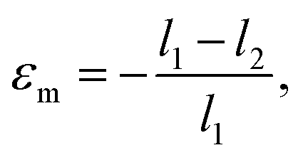 | (1) |
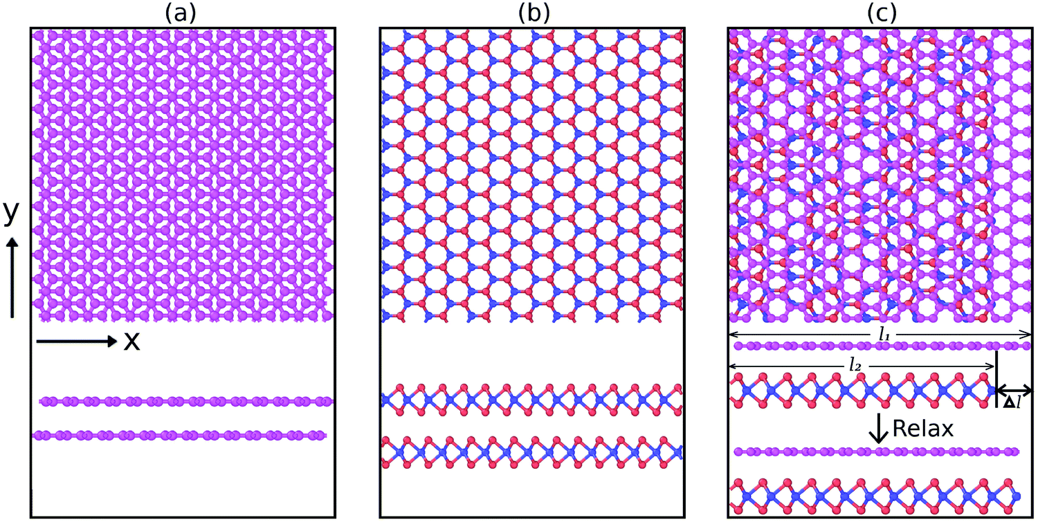 | ||
| Fig. 1 Studied bilayer structures: (a) graphene/graphene structure; (b) MoS2/MoS2 structure; (c) graphene/MoS2 heterostructure. The x direction corresponds to the armchair direction, and the y direction corresponds to the zigzag direction. l1 and l2 are the lengths of the graphene layer and the MoS2 layer, respectively, and Δl is their length difference resulting in the misfit strain in the relaxed configuration of the graphene/MoS2 heterostructure. | ||
The carbon–carbon interaction is described by the second-generation Brenner (REBO-II) potential,38 while the MoS2 interatomic interactions are described by the Stillinger–Weber potential39 with parameter values from recent work.40 The interlayer interactions between graphene/graphene, MoS2/MoS2 and graphene/MoS2 are described by the Lennard-Jones potential, for which the distance and energy parameters are given in Table 1.
| Structure | ε [meV] | σ [Å] | Cutoff [Å] |
|---|---|---|---|
| Graphene/graphene | 2.96 | 3.382 | 10.0 |
| MoS2/MoS2 | 23.6 | 3.18 | 10.0 |
| Graphene/MoS2 | 3.95 | 3.625 | 10.0 |
All the MD simulations were performed using the LAMMPS package,42 and the OVITO package was used for visualization.43 The standard Newtonian equations of motion were integrated in time using the velocity Verlet algorithm with a time step of 1 fs. Periodic boundary conditions were used in the two in-plane directions, while the free boundary condition was used in the out-of-plane direction.
The thermal expansion was simulated as follows. First, the structure was minimized to its lowest-energy configuration using the conjugate gradient algorithm and then optimized for 200 ps within the NPT ensemble (i.e. the number of particles N, the pressure P and the temperature T of the system were constant) at the desired temperature at zero pressure. Second, the structure was allowed to evolve for 1 ns within the NPT ensemble, and the size of the structure was averaged during this step. The averaged size L at different values of T was then used to compute the TEC. The standard deviation error ΔL in the time average gives the error for the size.
3 Results and discussion
3.1 Simulation results
Fig. 2 shows the temperature dependence of the sizes of the graphene/graphene and MoS2/MoS2 bilayer structures. Fig. 2(a) shows the temperature dependence for the two lateral dimensions of the graphene/graphene structure with an approximate size of 200 Å × 200 Å. The relationship between length and temperature is fitted with a linear function with a slope of dL/dT. The one-dimensional TEC α is calculated as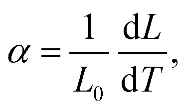 | (2) |
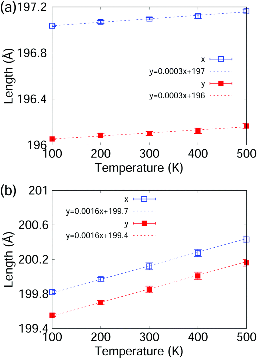 | ||
| Fig. 2 Temperature dependence of length of (a) graphene/graphene structure and (b) MoS2/MoS2 structure. The points are the numerical results, while the dashed lines are the fitting results. | ||
Thermally induced ripples are important in 2D materials such as the graphene/graphene and MoS2/MoS2 bilayer structures. Because of such ripples, the thermal properties of the atomic layers can be size-dependent. Indeed, Fig. 3 shows that the TEC depends on the size of these two bilayer structures; in particular, it is obviously larger in smaller structures. All the structures simulated in this figure are square with almost the same size in the two lateral dimensions. The size effect can be understood as follows: the thermally induced ripples become taller at higher temperature, thereby decreasing the in-plane size of the bilayer structure; consequently, the ripples act to reduce the TEC. Note that in graphene, the thermally induced ripples have an intrinsic length of 30–60 Å.46 In graphene/graphene structures smaller than that intrinsic size, the thermally induced ripples are weakened by size confinement, so their negative effect is weaker in smaller structures. Actually, Fig. 3 shows that the size effect becomes less important for graphene/graphene structures larger than 60 Å, which further confirms the ripple-based mechanism for the size effect. Therefore, the TEC decreases with increasing size of the graphene/graphene structure. Similar arguments pertain for the size dependence of the TEC of MoS2/MoS2 structures.
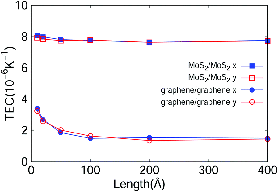 | ||
| Fig. 3 Size dependence of thermal expansion coefficient (TEC) of graphene/graphene (circles) and MoS2/MoS2 (squares) structures. The TEC is isotropic in the in-plane directions. | ||
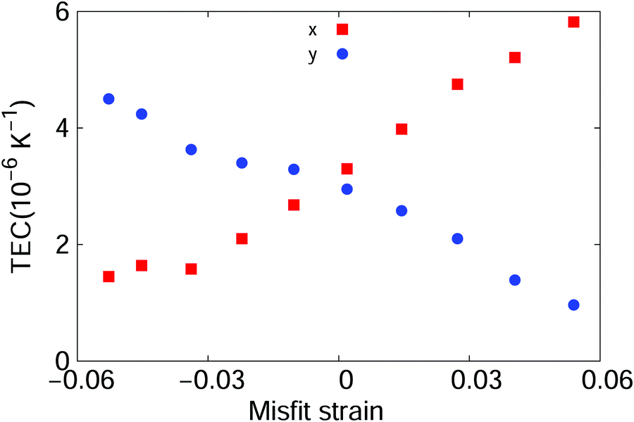
From the above, we have learned that the TEC of the MoS2/MoS2 structure is larger than that of the graphene/graphene structure, and the thermally induced ripples have a negative effect on the TEC. We now study the TEC of graphene/MoS2 heterostructures. Fig. 4 shows the TEC of graphene/MoS2 heterostructures with different misfit strains. The horizontal axis represents the misfit strain calculated by eqn (1), and the vertical axis represents the corresponding TEC values. Two sets of heterostructures with quite different dimensions are simulated here. In the first set, the length along the y direction is 199.2 Å and 199.6 Å for the graphene and MoS2 layers, respectively (denoted by ly = 200 in Fig. 4); these sizes were chosen to minimize the misfit strain in the y direction. For the graphene and MoS2 layers, the length along the x direction is between 187 Å and 213 Å so that the misfit strain is between −6.2% and 6.6%. In the second set of heterostructures, the length along the y direction is 49.2 Å and 49.9 Å for the graphene and MoS2 layers, respectively (denoted by ly = 50 in Fig. 4). For the graphene and MoS2 layers, the lengths along the x direction are in the wide range of 50–105 Å.
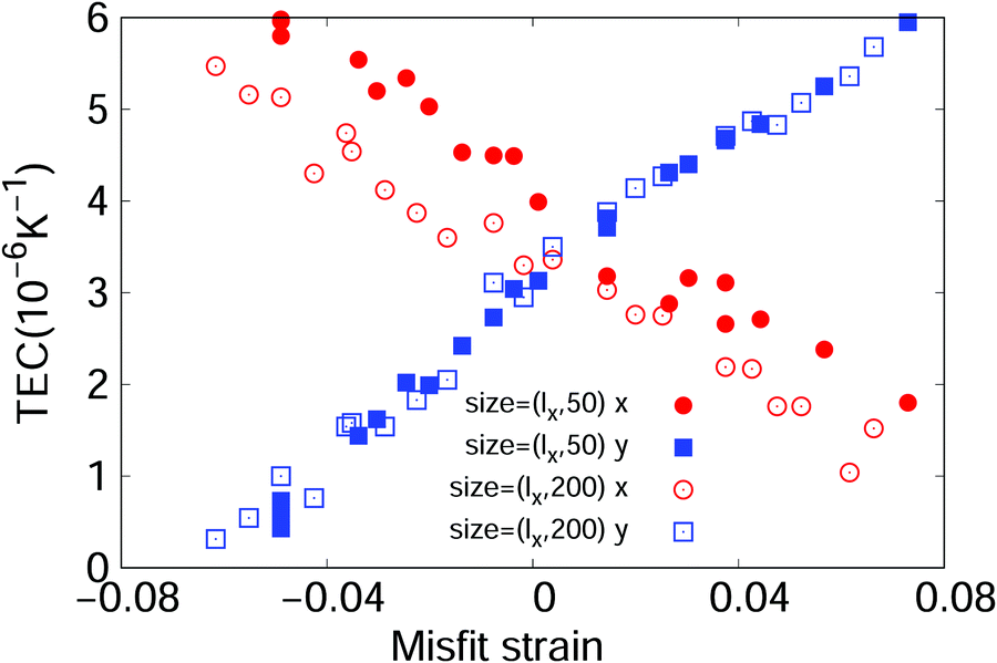 | ||
| Fig. 4 TEC for graphene/MoS2 heterostructures with different misfit strains. There are two sets of structures with ly ≈ 50 Å and ly ≈ 200 Å, respectively. The length lx is varied to tune the misfit strain value. The TEC along the x (resp. y) direction is displayed by circles (resp. rectangles). | ||
The results in Fig. 4 show that the TEC can be tuned linearly from 1 × 10⁻⁶ K−1 to 6 × 10⁻⁶ K−1 by the misfit strain. More specifically, with increasing misfit strain, the TEC along the x direction decreases linearly while that along the y direction increases linearly. The effect of the misfit strain is quite robust given that similar phenomena are observed for both sets of heterostructures with quite different lateral dimensions.
3.2 Discussion
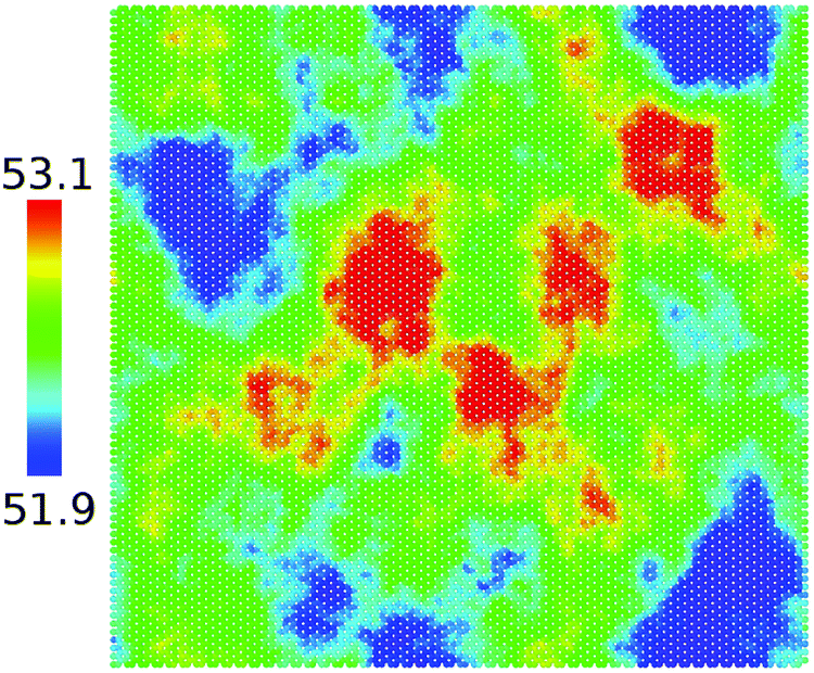
Recall that thermally induced ripples play an important role in the thermal and mechanical properties of quasi-2D atomic layers such as graphene/MoS2 heterostructures; in particular, as shown above, they have a negative effect on the TEC. Previous studies have shown mechanical strain to be an efficient means of tuning the thermally induced ripples in atomic-layered structures.47–50 Therefore, it is quite possible that the misfit strain (a specific mechanical strain) could affect the thermally induced ripples and eventually influence the TEC of the graphene/MoS2 heterostructure, and so we investigate how the misfit strain affects the thermally induced ripples.As defined in eqn (1), with positive misfit strain (εm > 0), the graphene layer is stretched while the MoS2 layer is compressed. Upon thermal vibration, the compressed MoS2 layer buckles slightly, leading to buckling of the whole heterostructure because the graphene layer is much softer than the MoS2 layer, as shown in Fig. 5(a), where the misfit strain is εm = 6.2%. The structure with large misfit strain has anisotropic ripples along the two in-plane directions, where the structure is buckled slightly along the x direction.
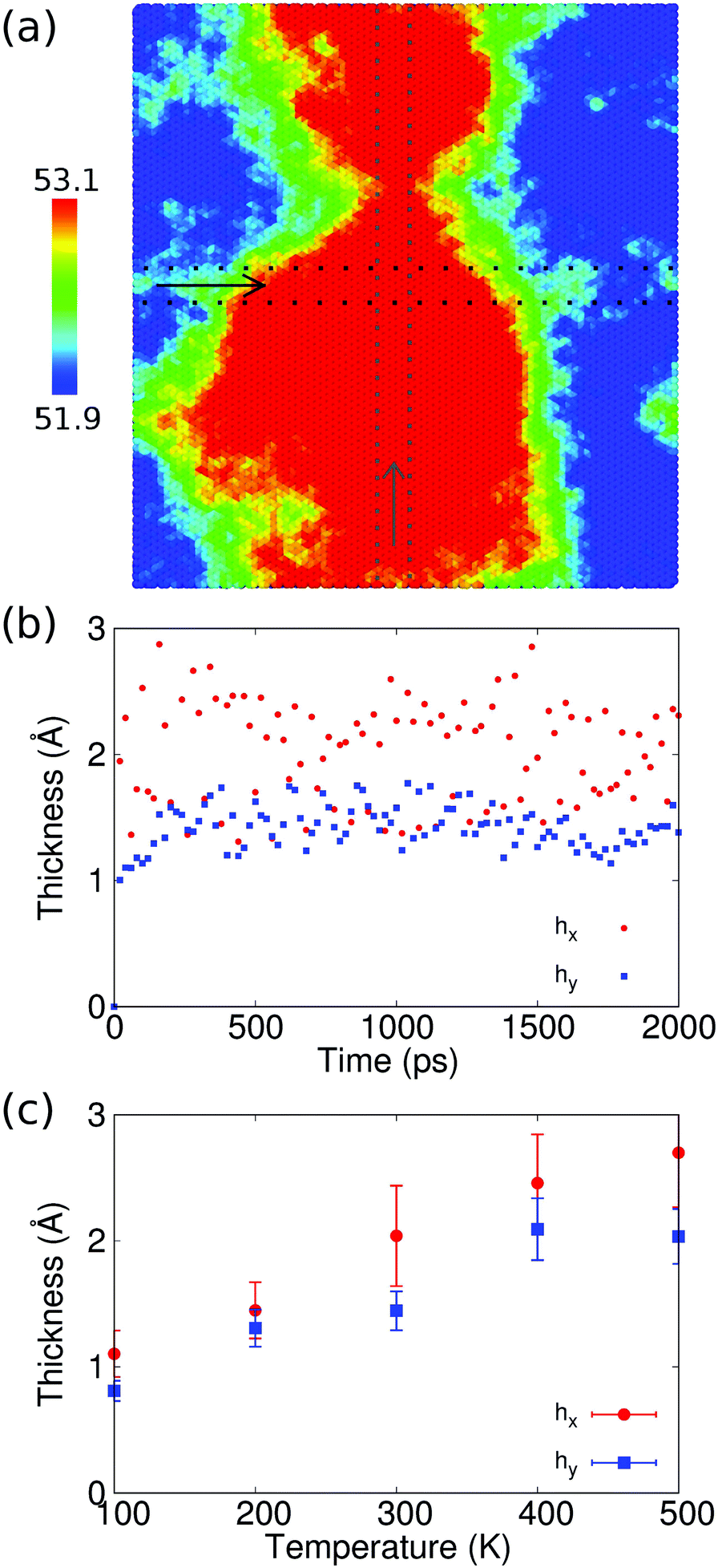 | ||
| Fig. 5 Ripples in graphene/MoS2 van der Waals (vdW) heterostructure with εm = 6.2%: (a) top view of distribution of ripples at 300 K; the colour bar represents the z coordinate of each atom; (b) time history of effective thickness of graphene/MoS2 heterostructure at 300 K; (c) temperature dependence of averaged effective thickness of graphene/MoS2 heterostructure; the average thickness along the x direction (red points) is larger than that along the y direction (blue points). | ||
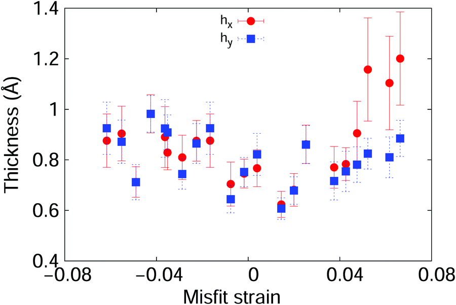
The effect of misfit strain on the ripples can be quantified further by introducing the effective thicknesses hx and hy along the x and y directions, respectively. We take hx as the example to introduce the calculation details. Scanning Fig. 5(a) from left to right along the x direction gives the minimum (zmin) and maximum (zmax) values of the z coordinate, and the thickness along the x direction is hx = zmax − zmin. Similarly, hy is calculated by scanning along the y direction. The thicknesses for the structure in Fig. 5(a) are hx = 2.04 Å and hy = 1.45 Å. The effective thickness is anisotropic along these two in-plane directions, which truly represents the major feature of this structure. Fig. 5(b) shows the time histories of the effective thicknesses at room temperature: the graphene/MoS2 heterostructure with a large misfit strain of 6.2% has a larger effective thickness along the x direction than along the y direction. The effective thickness can be obtained by averaging over time; for example, we obtain hx = 2.04 ± 0.39 Å and hy = 1.45 ± 0.15 Å for the structure in Fig. 5(a), where the errors are the standard deviation errors in the average over time. The temperature dependence of the effective thickness is shown in Fig. 5(c); the effective thickness increases with increasing temperature because of the stronger thermal vibrations at higher temperatures. Furthermore, Fig. 6 shows that the effective thickness is anisotropic for structures with misfit strain above 4%, where hx is obviously larger than hy.
 | ||
| Fig. 6 Effective thicknesses hx and hy along x and y directions, respectively, for graphene/MoS2 heterostructure with different misfit strains at 100 K. hx is obvious larger than hy when the misfit strain exceeds 4%. | ||
The misfit-strain-induced ripples along the x direction cause a strong reduction of the TEC along the x direction, leading to the decrease of the TEC along the x direction with increasing misfit strain in Fig. 4. In contrast, the buckling along the x direction can weaken the ripples along the y direction, so the y-directional TEC increases with increasing misfit strain.
As defined in eqn (1), with negative misfit strain (εm < 0), the graphene layer is compressed while the MoS2 layer is stretched. The buckling of the graphene/MoS2 heterostructure is induced mainly by that of the Mos2 layer because the critical buckling strain for the MoS2 layer is larger than that for the graphene layer. For positive misfit strain, the MoS2 layer is stretched by the misfit strain and so does not buckle easily; consequently, the whole heterostructure does not buckle, even though the graphene layer is compressed by the misfit strain. Fig. 7 confirms that the graphene/MoS2 heterostructure does not buckle with a negative misfit strain of εm = −6.6%, so the buckling is not the source of the effect of negative misfit strain.
 | ||
| Fig. 7 Thermal vibrations in graphene/MoS2 vdW heterostructure with εm = −6.6%. The colour bar represents the z coordinate of each atom. No buckling occurs. | ||
Instead of the buckling mechanism, several other competing mechanisms may co-exist for the effect of negative misfit strain in Fig. 4. On one hand, the compressive misfit strain on the graphene layer acts to reduce the TEC along the x direction, this being because compression is more likely to induce ripples that affect the TEC negatively. On the other hand, the positive misfit strain on the MoS2 layer acts to increase the TEC along the x direction, this being because the nonlinear effect strengthens upon stretching and enhances the TEC. Our MD results show that the second mechanism surpasses the first mechanism, so the TEC along the x direction increases with decreasing misfit strain for εm < 0. One possible reason is that the TEC for MoS2 is much larger than that for graphene, as can be seen from Fig. 3, so the second mechanism (on MoS2) is more important than the first mechanism (on graphene).
In all of the graphene/MoS2 heterostructures above, the misfit strain along the y direction is almost zero, while that along the x direction is varied to tune the TEC. Fig. 8 shows a similar misfit-strain effect on the TEC of the graphene/MoS2 heterostructure with varying misfit strain along the y direction.
 | ||
| Fig. 8 TEC for graphene/MoS2 heterostructure with varying misfit strain along y direction. The misfit strain along the x direction is almost zero (−0.2%). The x axis represents the misfit strain along the y direction, and the y axis represents the TEC. | ||
4 Conclusion
In the present study, MD simulations were used to investigate how misfit strain affects the TEC of the graphene/MoS2 heterostructure. The TEC can be tuned in a wide range from 1 × 10⁻⁶ K−1 to 6 × 10⁻⁶ K−1 by the misfit strain, and this effect is insensitive to the size or direction of the heterostructure. More specifically, the TEC along the misfit-strain direction decreases linearly with increasing misfit strain. We explored several possible underlying mechanisms for the misfit-strain effect on the TEC, and we showed that the misfit strain can tune the thermally induced ripples, thereby exerting strong effects on the TEC of the heterostructure. These results provide an effective way to manipulate the TEC of vdW heterostructures through misfit-strain engineering.Conflicts of interest
There are no conflicts to declare.Acknowledgements
This work was supported by the National Natural Science Foundation of China (Grant No. 11822206 and 12072182) and the Innovation Program of the Shanghai Municipal Education Commission (Grant No. 2017-01-07-00-09-E00019).References
- A. K. Geim and K. S. Novoselov, Nat. Mater., 2007, 6, 183 CrossRef CAS.
- A. A. Balandin, Nat. Mater., 2011, 10, 569 CrossRef CAS.
- C. Lee, X. Wei, J. W. Kysar and J. Hone, Science, 2008, 321, 385 CrossRef CAS.
- Y. An, Y. Hou, K. Wang, S. Gong and R. Wu, Adv. Funct. Mater., 2020, 30, 2002939 CrossRef CAS.
- Y. Liu, N. O. Weiss, X. Duan, H. C. Cheng and X. Duan, Nat. Rev. Mater., 2016, 1, 16042 CrossRef CAS.
- S. Singh, C. Espejo and A. H. Romero, Phys. Rev. B, 2018, 98, 155309 CrossRef CAS.
- Y. An, K. Wang, G. Shijing, Y. Hou, C. Ma, M. Zhu, C. Zhao, T. Wang, H. Wang and R. Wu, et al. , NPJ Comput. Mater., 2021, 7, 45 CrossRef CAS.
- A. A. Balandin, S. Ghosh, W. Bao, I. Calizo, D. Teweldebrhan, F. Miao and C. N. Lau, Nano Lett., 2008, 8, 902 CrossRef CAS PubMed.
- W. J. Yu, Q. A. Vu, H. Oh, H. G. Nam, H. Zhou, S. Cha, J. Y. Kim, A. Ca Rvalho, M. Jeong and H. Choi, Nat. Commun., 2016, 7, 13278 CrossRef CAS PubMed.
- Y. Zhong, G. Liu, J. M. Khan and A. A. Balandin, Nat. Commun., 2012, 3, 827 CrossRef PubMed.
- Q. Liu, B. Cook, M. Gong, Y. Gong, D. Ewing, M. Casper, A. Stramel and J. Wu, ACS Appl. Mater. Interfaces, 2017, 9, 12728 CrossRef CAS PubMed.
- R. Frisenda, E. Navarro-Moratalla, P. Gant, D. P. D. Lara, P. Jarillo-Herrero, R. V. Gorbachev and A. Castellanos-Gomez, Chem. Soc. Rev., 2018, 47, 53 RSC.
- L. Chen, X. Li, C. Huang, S. Hu and W. Han, J. Mater. Chem. C, 2020, 8, 4021 RSC.
- C. Wu, G. Zhao, X. Yu, C. Liu, P. Lyu, G. Maurin, S. Le, K. Sun and N. Zhang, Chem. Eng. J., 2021, 412, 128736 CrossRef CAS.
- Q. H. Wang, K. Kalantar-Zadeh, A. Kis, J. N. Coleman and M. S. Strano, Nat. Nanotechnol., 2012, 7, 699 CrossRef CAS.
- L. Britnell, R. Gorbachev, R. Jalil, B. Belle, F. Schedin, A. Mishchenko, T. Georgiou, M. Katsnelson, L. Eaves and S. Morozov, et al. , Science, 2012, 335, 947 CrossRef CAS.
- N. Mounet and N. Marzari, Phys. Rev. B: Condens. Matter Mater. Phys., 2005, 71, 205214 CrossRef.
- K. V. Zakharchenko, M. I. Katsnelson and A. Fasolino, Phys. Rev. Lett., 2009, 102, 046808 CrossRef CAS.
- M. Pozzo, D. Alfe, P. Lacovig, P. Hofmann, S. Lizzit and A. Baraldi, Phys. Rev. Lett., 2011, 106, 135501 CrossRef PubMed.
- S. Mann, R. Kumar and V. K. Jindal, RSC Adv., 2017, 7, 22378 RSC.
- P. Anees, M. C. Valsakumar and B. K. Panigrahi, Phys. Chem. Chem. Phys., 2017, 19, 10518 RSC.
- F. H. Liang, L. G. Peng and Z. Zhi, Phys. Rev. B: Condens. Matter Mater. Phys., 2014, 90, 045409 CrossRef.
- G. López-Polín, M. Ortega, J. Vilhena, I. Alda, J. Gomez-Herrero, P. Serena, C. Navarro and R. Pérez, Carbon, 2017, 116, 670 CrossRef.
- D. Yoon, Y. W. Son and H. Cheong, Nano Lett., 2011, 11, 3227 CrossRef CAS.
- G. A. McQuade, A. S. Plaut, A. Usher and J. Martin, Appl. Phys. Lett., 2021, 118, 203101 CrossRef CAS.
- L. Zhang, Z. Lu, Y. Song, L. Zhao, B. Bhatia, K. R. Bagnall and E. N. Wang, Nano Lett., 2019, 19, 4745 CrossRef CAS.
- G. Anemone, A. Al Taleb, A. Castellanos-Gomez and D. Farias, 2D Mater., 2018, 5, 035015 CrossRef.
- Z. Lin, W. Liu, S. Tian, K. Zhu and Y. Yang, Sci. Rep., 2021, 11, 7037 CrossRef CAS PubMed.
- K. H. Michel, S. Costamagna and F. M. Peeters, Phys. Status Solidi, 2015, 252, 2433 CrossRef CAS.
- W. Bao, F. Miao, Z. Chen, H. Zhang, W. Jang, C. Dames and C. N. Lau, Nat. Nanotechnol., 2009, 4, 562 CrossRef CAS PubMed.
- J. W. Jiang and H. S. Park, Appl. Phys. Lett., 2014, 105, 033108 CrossRef.
- Y. C. Lin, C. Y. Chang, R. K. Ghosh, J. Li, H. Zhu, R. Addou, B. Diaconescu, T. Ohta, X. Peng and N. Lu, et al. , Nano Lett., 2014, 14, 6936–6941 CrossRef CAS.
- L. Y. Li and M. W. Zhao, J. Phys. Chem. C, 2014, 118, 19129 CrossRef CAS.
- Z. H. Ni, W. Chen, X. F. Fan, J. L. Kuo and Z. X. Shen, Phys. Rev. B: Condens. Matter Mater. Phys., 2008, 77, 115416 CrossRef.
- J. Chaste, A. Missaoui, A. Saadani, D. G. Sanchez and A. Ouerghi, ACS Appl. Nano Mater., 2018, 1, 6752 CrossRef CAS.
- S. Shivaraman, J. Jobst, D. Waldmann, H. B. Weber and M. G. Spencer, Phys. Rev. B: Condens. Matter Mater. Phys., 2013, 87, 195425 CrossRef.
- J. D. He and J. W. Jiang, Nanotechnol, 2019, 30, 265701 CrossRef CAS.
- D. W. Brenner, O. A. Shenderova, J. A. Harrison, S. J. Stuart, B. Ni and S. B. Sinnott, J. Phys.: Condens. Matter, 2002, 14, 783 CrossRef CAS.
- F. H. Stillinger and T. A. Weber, Phys. Rev. B: Condens. Matter Mater. Phys., 1985, 31, 5262 CrossRef CAS PubMed.
- J. W. Jiang, Acta Mech. Solida Sin., 2019, 32, 17 CrossRef.
- J. W. Jiang and H. S. Park, J. Appl. Phys., 2015, 117, 124304 CrossRef.
- S. Plimpton, J. Comput. Phys., 1995, 117, 1 CrossRef CAS.
- A. Stukowski, Model. Simul. Mater. Sci. Eng., 2009, 18, 015012 CrossRef.
- K. V. Zakharchenko, J. H. Los, M. I. Katsnelson and A. Fasolino, Phys. Rev. B: Condens. Matter Mater. Phys., 2010, 81, 235439 CrossRef.
- Z. Y. Wang, Y. L. Zhou, X. Q. Wang, F. Wang, Q. Sun, Z. X. Guo and Y. Jia, Chin. Phys. B, 2015, 24, 026501 CrossRef.
- P. Gallagher, M. Lee, F. Amet, P. Maksymovych, J. Wang, S. Wang, X. Lu, G. Zhang, K. Watanabe and T. Taniguchi, Nat. Commun., 2016, 7, 10745 CrossRef CAS PubMed.
- S. Hussain, A. Liaqat and M. A. Iqbal, Appl. Phys. Lett., 2020, 117, 153102 CrossRef CAS.
- J. Wang, R. R. Namburu, M. Dubey and A. M. Dongare, Sci. Rep., 2017, 7, 40862 CrossRef CAS PubMed.
- L. Kou, Y. Ma, S. C. Smith and C. Chen, J. Phys. Chem. Lett., 2015, 6, 1509 CrossRef CAS.
- F. Abualnaja, M. Hildebrand and N. M. Harrison, Comput. Mater. Sci., 2020, 173, 109422 CrossRef CAS.
Footnote |
| † Current institution: College of Mechanical and Electrical Engineering, Hebei Agricultural University, Baoding 071001, People's Republic of China. |
| This journal is © the Owner Societies 2022 |