
 Open Access Article
 This Open Access Article is licensed under a
 Creative Commons Attribution 3.0 Unported Licence
A purely ionic voltage effect soft triode†
Elalyaa
Mohamed
 a,
Sabine
Josten
a and
Frank
Marlow
*ab
a,
Sabine
Josten
a and
Frank
Marlow
*ab
aMPI für Kohlenforschung, Kaiser-Wilhelm-Platz 1, Mülheim an der Ruhr 45470, Germany. E-mail: marlow@mpi-muelheim.mpg.de
bCenter for Nanointegration Duisburg-Essen (CENIDE), University of Duisburg-Essen, Duisburg 47057, Germany
First published on 23rd March 2022
Abstract
We report on the construction and characterization of an ionic soft triode intended to be based on interfacial ion adsorption and redox oxidizer depletion. The soft triode was built in a simple manner with no need for sophisticated or expensive materials. It does not utilize the control of a semiconducting channel, but an electrolyte. In different electrical circuit configurations, it can show amplification or memory effects. The device had an electrical current amplification reaching 52 and memory effects in the electrical resistance lasting for up to 6 h. These values were achieved by tuning the electrode interface, the electrolyte and diffusion properties. They are promising for neuromorphic applications.
1 Introduction
Iontronics is a wide concept of controlling electronic devices using ions. The word became widely known in 2010 when a book with this word in its title was published.1 However, there have been several attempts in the direction of controlling electronics with electrolytes already in the past.2–4As ions move much slower than electrons, iontronic devices cannot compete with classical electronics in speed. On the other hand, iontronic devices are expected to open a new door for many applications due to their low cost, their potential coupling to biological systems, and their ability to carry chemical information that allows regulating selectively different functions and processes. Despite the outstanding performance of electronic devices, they also have limitations in using them as building blocks in so-called neuromorphic devices and systems. Iontronic devices may fill gaps here. Many of them were invented in the last few decades like ionic transistors5,6 ionic capacitors7 and ionic memory devices.
Ionic amplification was first recognized in a microfluidic ionic bipolar junction transistor.8 With an ionic bipolar transistor, the current gain reached 10, which was achieved by using an emitter gain voltage of 4 V. Ionic field effect transistors represent a class of ionic transistors where ionic or molecular species in micro or nanofluidic systems are controlled by an electric field on the gate electrode of the transistor.6,9 Most of these devices can be used as amplifiers. However, the channels in most of the mentioned transistors are semiconductors or semiconducting polymers that need sophisticated materials and construction methods. Although many ionic devices were developed, there is not much research on signal amplification in ionic systems yet. To improve their biological and chemical sensing, more ionic devices with amplification function would offer new solutions for low-cost devices.
Another important element in electronics and iontronics is the memory. There are many different types of new memory devices but the most interesting type seems to be the resistive switching memory, also called a memristor. A resistive switching memory is a device with low energy consumption, mostly fast operation and a simple structure.10–12 These memory devices are expected to open a new door for computing systems and biological applications.13 There are different working principles for this type of memory like electrochemical reactions,11 vacancy-based resistance changes/charge trapping,14 and phase-change materials.15 Most of the known resistive switching memory devices are built with a simple structure of an insulator between two metals (MIM).16 They show interesting non-linear behavior in circuits, but also some problems in stability and device integration.17,18
In this work, we introduce a new, purely ionic device with amplification behavior and memory functions which is called an ionic voltage effect soft triode (IVEST). This device is a simple electrochemical micro-cell which consists of a top electrode and two bottom electrodes. The basic idea of this device is to control the concentration and diffusion of ions by the voltage applied on the top electrode. This electrode is made of porous titania, a material which can adsorb ions depending on its potential. The advantages of this device are the ability to be used as an amplifier or a memory, the ease of manufacturing, the low power consumption and the avoidance of any ultra-pure semiconducting material. The need for eco-friendly devices is increasing and using abundant materials and less sophisticated manufacturing methods is a challenge nowadays. A drawback of the device seems to be the imperfect memory contrast; however, as in biological information processing, a very high contrast is not needed for many applications. We especially believe that this device can be used in neuromorphic applications.
2 Experimental details
2.1 Device construction
The general layout of the device is shown in Fig. 1. Single parts of the device as well as their fabrication methods were adapted from the elaborated and optimized construction of dye-sensitized solar cells. In solar cells, all parts are adjusted to each other. This explains the special selection of the electrolyte as well as of sealing materials. Essentially, the device consists of three electrodes, all based on stainless steel. Variations from the basic procedure are described in the ESI.† | ||
| Fig. 1 (A) Device construction, (B) device symbol, and (C) two-gate configuration. T, B1, and B2 are the names of the three electrodes as explained in the text. The idea of the device is the control of the current JBB (red arrow) by the potential VT. The top electrode (T) is made of porous TiO2, which can adsorb ions depending on its potential as it is used in the so-called dye-sensitized solar cells.20,23 For device characterization, a BB symmetric configuration with R1 = R2 = 2 kOhm was selected. | ||
2.2 Characterization methods
Different measurement configurations were used to characterize the device. These configurations are described in the ESI† (S2). The most important measurement to see both the memory function and the amplification behavior turned out to be the one shown in Fig. 2.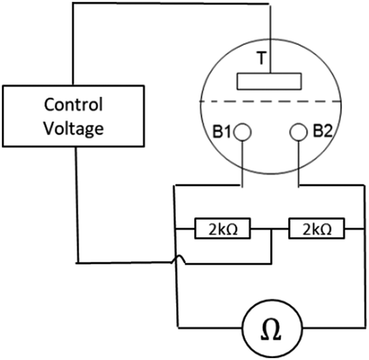 | ||
| Fig. 2 The Sym-BB-Ω measurement configuration. The resistance between the bottom electrodes is measured depending on the top voltage. The B-electrodes are symmetric with respect to the top voltage. | ||
Here the resistance between the two bottom electrodes RBB is measured (IDM93N, RS PRO GmbH). Typical test currents were 40 μA. Continuous as well as pulsed (typical time 1 s) measurements have been carried out.
For additional characterization, the current on the top electrode (Jtop) was measured by applying a fixed voltage between the two bottom electrodes (VBB) and using a JV analyzer. To characterize the output current (JBB), the top electrode was connected to the power supply and the bottom electrodes to the JV analyzer as shown in Fig. S2 (ESI†).
The thickness of the TiO2 layer of the electrodes was investigated with a SEM (TM3030, Hitachi).
3 Results
3.1 Basic characterization: the JJVV field
The device can be regarded as a 2-gate with input and output. Therefore, the device was characterized with different methods adapted from classical transistor measurements.The results in Fig. 3A reveal a strongly nonlinear dependence of the input current from the input voltage Vtop and a week dependence of the input current from VBB. This difference of sensitivity supports our selection of the input and output gate. The weak dependence of the input current on the output voltage means a low back-action. Fig. 3A shows the result at positive values of VBB only. The results for negative values can be found in the ESI.† They are nearly identical with only small indications for asymmetries. There were some small unavoidable asymmetries in the construction in the two bottom electrodes which may have led to small asymmetry in the results. Additionally, it is important to note that the input current is very low at Vtop = −0.37 V to 0.5 V. We call this range the low-input current (LIC) range.
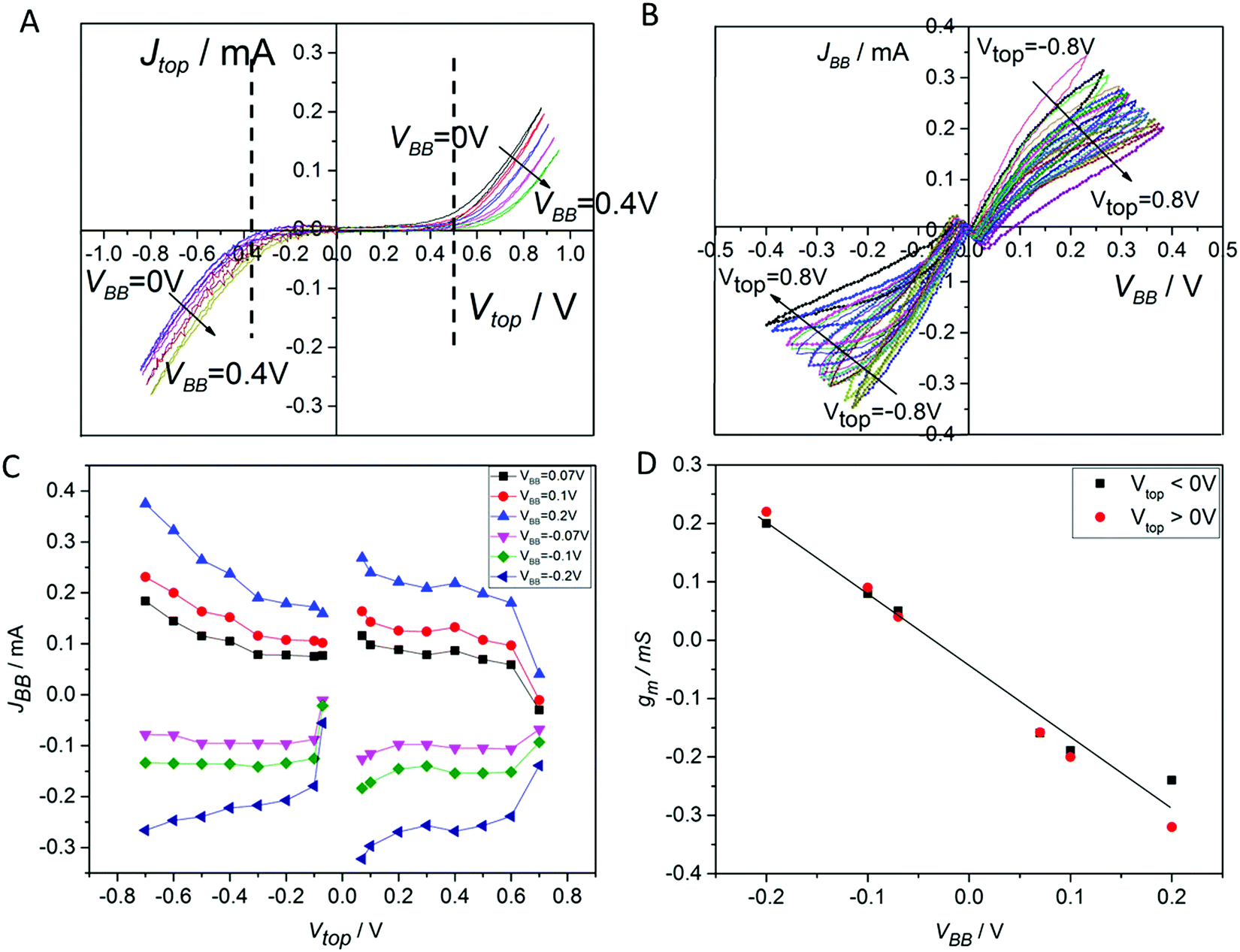 | ||
| Fig. 3 Basic characterization of a non-optimized IVEST (A) Sym-BB input characteristics. At the output constant VBB values were applied from 0 V to 0.4 V. The LIC range is indicated in the figure. (B) Sym-BB output characteristics. VBB was scanned by a JV measurement device whereas at the input fixed values of Vtop were applied from −0.8 V to 0.8 V. (C) Transfer curve. (D) Differential transconductance calculated from eqn (1) at small values of VBB. Investigated sample: 156. As shown in the ESI,† five similar samples have shown nearly the same characteristics. | ||
The output current JBB was measured. Generally, the output curves are nearly linear and resemble a resistor. However, this resistor of the output gate depends on the input. In Fig. 3B it is visible that the resistance increased by increasing Vtop. The voltage applied on the top electrode was kept lower than 1 V to avoid chemical reactions that may happen inside the system.
The magnitudes of the output current as well as of the output resistance represent a major difference of the IVEST in comparison to the other proposed ionic transistors.24 Varying the input voltage from 0 to −0.6 V causes a change in the output current by 0.1 mA at VBB = 0.2 V. This change in the output current is much higher than that in some known ionic transistors where the same change of input voltage causes a change in the output current of less than 0.002 mA at an output voltage of VD = 0.2 V.6
The output shows a visible hysteresis. This hysteresis can be attributed to several reasons, but the most important ones seem to be the delay in ion motion and ion redistribution. From the first look the hysteresis seems to be a drawback of the device intending amplification and switching applications, but at further investigations it will turn to be an interesting option of the device that will be discussed later in Section 3.4. There, we discuss useful memory effects which have been achieved by systematically increasing the hysteresis.
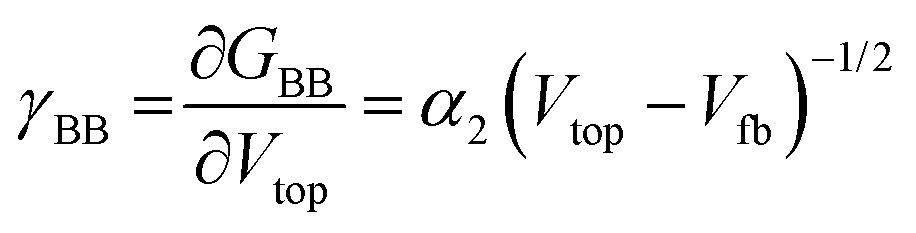
A transfer curve usually describes the interconnections of the input and output.21 In Fig. 3C, the output current was plotted at different input voltages Vtop (Fig. 3C). The output current started to change significantly at higher absolute values of Vtop. To evaluate the performance of the device in this range, the differential transconductance gm was calculated at different working points (i.e. at different Vtop and VBB values). The differential transconductance gm is defined by the following equation which deviates slightly from the frequently used21 non-differential value g′m = Iout/Vin:
 | (1) |
This enables the direct determination of gm from transfer curves. The resulting gm is shown in Fig. 3D. The values are significantly higher than the gm of known EDLTs with values of 0.04 and 0.1725,26 but lower than values for commercial electronic devices. We will discuss this issue below again. Here we also remark an interesting VBB dependence of the transconductance:
| gm = γBB × VBB | (2) |
This allows the introduction of the “specific differential transconductance” γBB. It reflects the nearly Ohmic output and represents a big difference to the conventional transistor and the MOSFET.
In the LIC range the input curve has revealed a high resistance in comparison to the output resistance RBB. When a slight change in the input current Jtop happened, a significant change in the output current JBB took place. This interconnection will be interpreted in the following section in terms of amplification.
3.2 Resistance control
Because the device has nearly Ohmic output characteristics, the characterization measurements can be simplified by using a standard Ohm-meter instead of a JV analyzer. The use of a stand-alone Ohm-meter not only shortens the measurements, but it also avoids the problem of possible ground interconnection effects between the different parts of the setup.When a positive voltage was applied on the top electrode, the resistance between the two bottom electrodes increased and when a negative voltage was applied on the top electrode, the resistance between the two bottom electrodes decreased as shown in Fig. 4A. Similar to Fig. 3A, Fig. 4A can be split into two parts, the middle part where Vtop = −0.37 V to 0.5 V and the corresponding outer part. In the middle part, the change in resistance is low. To describe the relationship between the output and the input, the ratio between Jtop and JBB was investigated based on the amplification definition described in eqn (3). We call it current amplification or J-amplification. Eqn (4) represents the relationship of the amplification to the system parameters at a certain working point (WP) (see the ESI†).
 | (3) |
 | (4) |
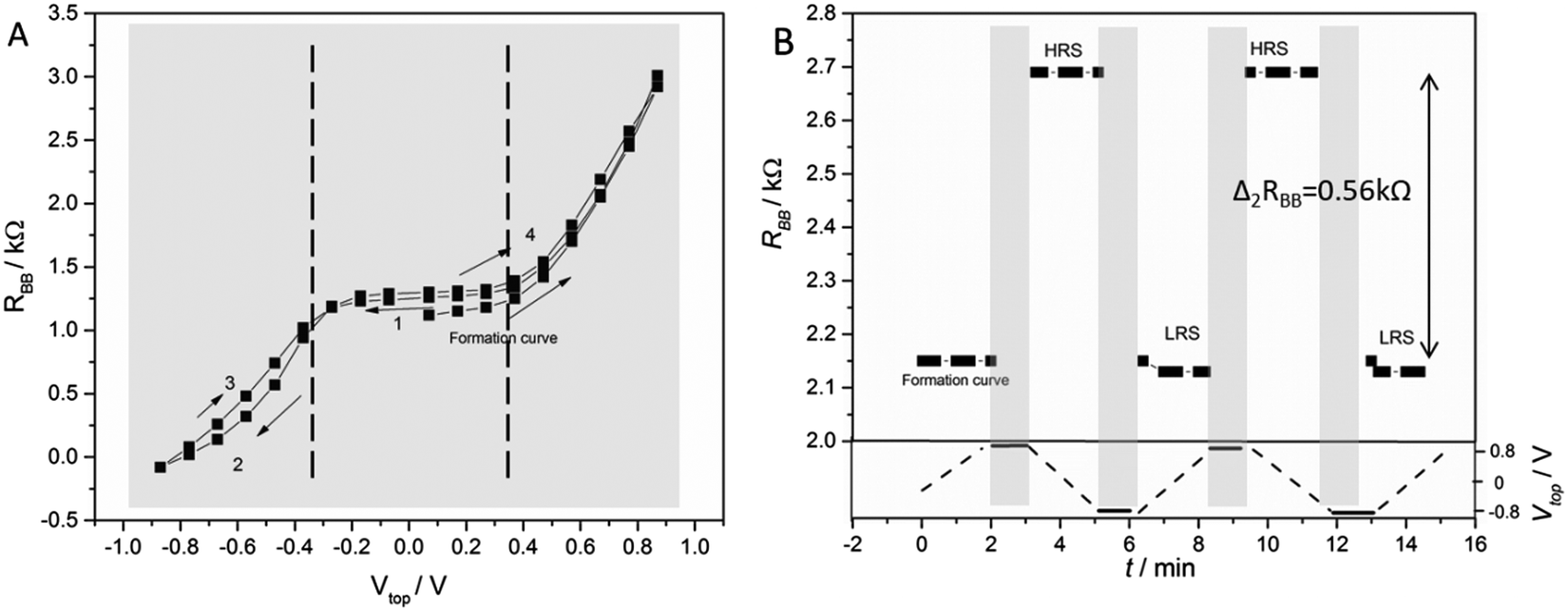 | ||
| Fig. 4 (A) The BB resistance at permanent control voltage measured in a pulsed manner with about 10 s waiting time after every Vtop change (sample 274). When a positive voltage is applied on the top electrode, RBB increases and when a negative Vtop is applied it decreases. The dashed lines indicate the range of low top-electrode current (see the ESI†). (B) Switching measurements with a voltage protocol shown in the lower part of the diagram (sample 285). A positive voltage was applied on the top electrode for 1 min. Then, the RBB under open top circuit conditions was measured for 2 min. This process was repeated with negative Vtop. A difference of resistances of ΔRBB = 0.56 kΩ was found. A high and low resistance state (HRS and LRS, respectively) is clearly visible. | ||
Interestingly, γBB can also be determined from the output resistance measurement namely as the differential quotient between the output conductivity and the top voltage as used in the ESI† (eqn S4). Therefore, one has two possibilities for γBB determination, either from the transfer curve or from the transfer conductance which is measured utilizing a different setup (Fig. 2). The calculations and measurements of γBB and Gd,top are described in the ESI.†
The best J-amplification after optimization was = −52 at the working point WP1 = (−0.37 V, 0.25 V). Here, the first value of this pair WP = (Vtop, VBB) describes the input voltage and the second one the output voltage.
The outer part of the graph (i.e. the non-LIC range) is defined by high |Vtop| values when either 0.5 V < Vtop or Vtop < −0.37 V. In these two ranges, the output resistance showed a rapid change when changing Vtop. In addition, the hysteresis becomes visible in most curves when this range of voltage is touched. Likely, these effects are caused by a relatively low input current. A high input current may cause ion redistribution and non-equilibrium states. These states can be responsible for the hysteresis which could possibly lead to a useful memory effect.
To obtain a deeper insight into the hysteresis and memory behaviour, a special experiment was developed using a control voltage protocol as shown in Fig. 4B. In this experiment, no voltage was applied on the top electrode (Vtop = open) during a certain “readout time”. The resistance was measured in a pulsed manner, i.e. with minimal currents between the B electrodes. The readings were taken each 10 s for 2 min (read-out time). Then, a positive voltage was applied on the top electrode (Vtop = 0.8 V) for 1 min (writing period). After this minute, the voltage applied on the top electrode was switched off (Vtop = open) and, again, the RBB readings were taken each 10 s for 2 min. Then, in another writing period, a negative voltage was applied on the top electrode for 1 min (Vtop = −0.8 V). After that, the resistance readings were taken again for 2 min.
Obviously, the IVEST can remember the “writing” during the readout periods. The device is either in a high or in a low resistance state (HRS or LHS, respectively). Within these states, there are small changes as well, but the memory character is not destroyed. In detail, one finds that the resistance readings showed a slight increase in the LRS with time and a slight decrease in the HRS.
As visible, the two states shown in Fig. 3B are fairly stable and, therefore, represent a useful memory behavior of the device. The difference between the two states reached values up to ΔRBB = 0.56 kΩ in this experiment. Another measure of the memory contrast is the ratio between the resistance of the HRS and the LRS which can be expressed by
 | (5) |
A value of about 1.3 was found for some devices as described below.
3.3 Amplification tuning
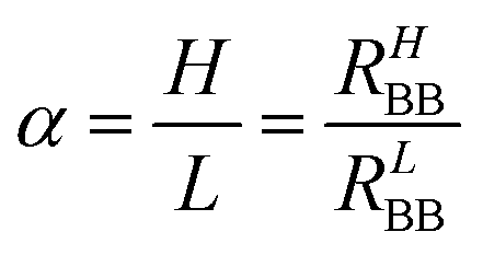
In order to investigate the nature of the amplification process and to explore the possibilities of an application, the variation of the amplification values by device variation was investigated. Two factors that were expected to have a big effect on the amplification were investigated. In addition, a working point WP1 at Vtop = −0.37 V and VBB = 0.25 V was selected for the following discussion. At this point one has the maximum amplification effects among our measured values.The first factor important for the amplification is the electrolyte concentration Xe (Fig. 5A and B). A series of diluted electrolytes were tested as shown in Fig. 5A. The results showed an increase in the resistance as the electrolyte was diluted. This can be attributed to fewer amounts of ions in the electrolyte. The amplification increased by increasing the concentration of the electrolyte until it reached the highest value at Xe = 0.6 and then it decreased as shown in Fig. 5B.
 | ||
| Fig. 5 Tuning of device parameters. (A) Effect of electrolyte dilution on RBB measured using a pulsed DC resistance measurement. (B) Calculated amplification at WP1 based on eqn S4 (ESI†), at different electrolyte concentrations. (C) Calculated amplification at different TiO2 thicknesses, determined analogously as in (A and B). The thickness scale was constructed from two SEM investigations of the electrodes. | ||
Another factor that affects the amplification is the thickness of the TiO2 layer on the top electrode tuned by XTiO2. As shown in Fig. 5C the tuning curve exhibits a maximum at the thinnest TiO2 layers. The negative current amplification reaches 52 at XTiO2 = 0.5. It seems that high amounts of the semiconductor at the top electrode are not beneficial for the amplification. One may correlate this fact with the amount of dead material. When the thickness of the TiO2 layer on the top electrode increases, more and more parts of the material are not in electrical contact with the metal mesh (“dead material”). The dead material can however adsorb electrolyte ions. Because they have no electrical contact with the electrode, they have no beneficial effect on the amplification. These ions are lost for the other processes. Thinner TiO2 layers are technically not possible at the moment. However, one can expect a further increase of the amplification at thinner layers.
3.4 Memory tuning
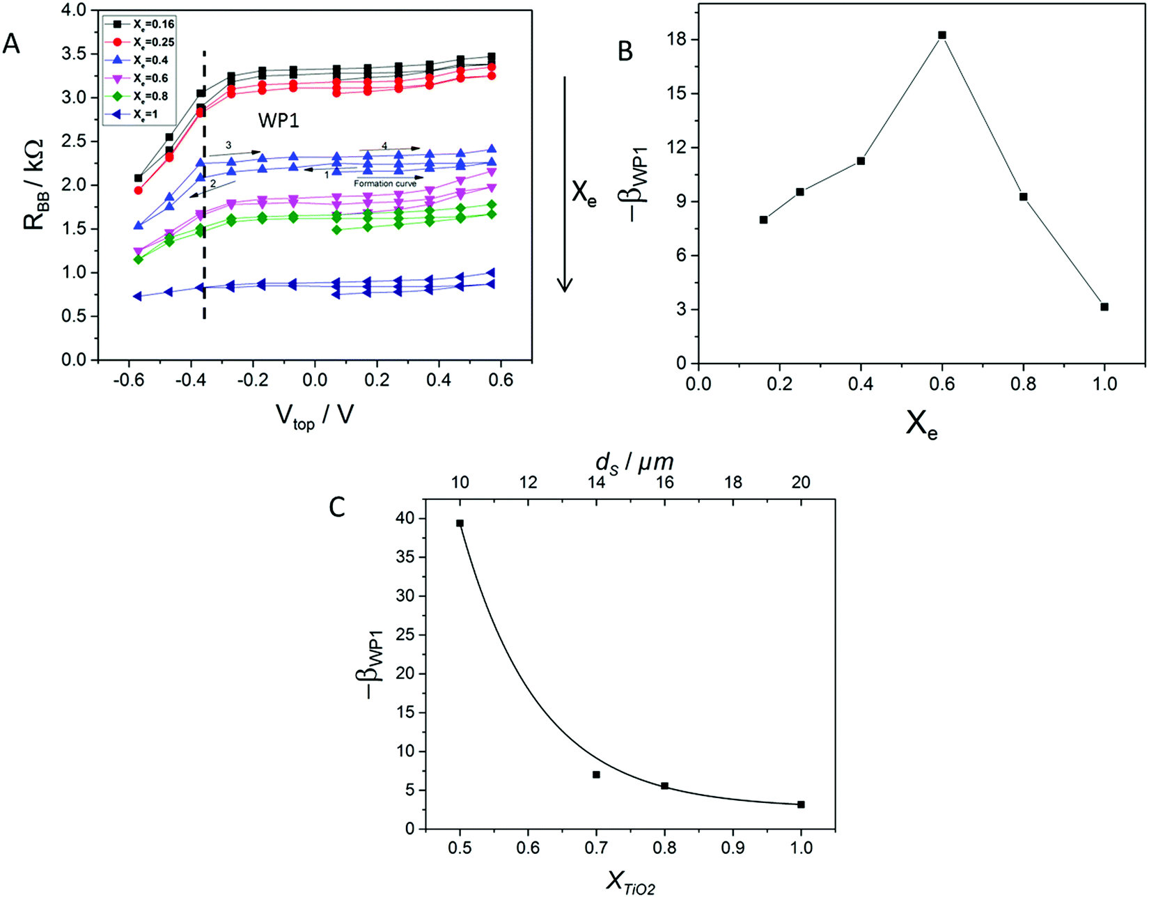
In Fig. 4A, a hysteresis has appeared when the top voltage exceeded the LIC region. This hysteresis indicates a possible memory effect. Enlarging this hysteresis was, therefore, the way for optimizing this potential memory. Finally two properties, the resistance contrast Δ2RBB and the stability time τ2, were used to characterize the efficiency of the memory. The stability time is the time that the two metastable states require to reach an equilibrium state. The difference of resistance between the HRS and the LRS after two minutes, Δ2RBB, was used to characterize the memory contrast.As the adsorption of the ions on the TiO2 layer likely plays a role in the mechanism of the device (see Section 4.2), the behavior of the IVEST was investigated at different electrode thicknesses realized by different concentrations of TiO2 in the dip-coating suspension. In Fig. 6A one can see that Δ2RBB moderately increased by decreasing the concentration of TiO2. This increase in Δ2RBB could likely be attributed to the decrease of the dead material or the rim on the top electrode.
 | ||
| Fig. 6 (A) Effect of TiO2 thickness on Δ2RBB. (B) Effect of electrolyte concentration on Δ2RBB. (C) Effect of membrane pore size on Δ2RBB. (D) Effect of membrane pore size on the stability. There is a big increase in τ2 when a membrane with a small pore size is used for the separation the device parts. The solid lines are guides to the eye. | ||
The second factor that affects Δ2RBB is the electrolyte. The difference between the two switching states Δ2RBB increased when the electrolyte was diluted (Fig. 6B).
The pore size of the membrane separating the device parts is also expected to have an influence on the memory behavior. This was indeed found. As the pore size decreased, Δ2RBB showed an increase. The factor that affects the stability time the most was also found to be the pore size of the membrane. By decreasing the pore size, τ2 increased. There was a big difference in τ2 when using a membrane with 150 μm pore size and membranes with pore sizes < 1.5 μm.
Based on the previous results, an optimized cell for memory effects was built with Xe = 0.16, XTiO2 = 0.5, and a spacer of 1.2 μm pore size. In the case of an optimized cell, values of Δ2RBB = 0.56 kΩ and τ2 = 5.8 h were found, leading to a contrast factor of α = 1.28. This cell is also shown in Fig. 4B.
4 Discussion
4.1 Working points and amplification mechanism
The results show that the amplification is strongly WP-dependent and that a working point WP1 with Vtop = −0.37 V seems to be optimal to have a maximal amplification for the investigated voltages. How can this be understood?When the semiconductor material comes in contact with the electrolyte, an electronic depletion zone is likely created in the semiconductor as shown in Fig. 7. This picture reminds on the Schottky contact, but here the Fermi energy of the metal is replaced by the redox potential of the electrolyte.27 This depletion zone near the electrolyte represents a positive charge. The electrolyte compensates this charge by forming different ionic layers. These layers must contain just the opposite ionic excess charge as the positive charge of the semiconductor. In addition, the ionic layers must contain a lot of additional electrolyte ions for screening all these charges. This enhanced concentration of ions near the electrode surface can be interpreted as variable storage. The amount of ions stored in this layer will be missing in the B-part of the IVEST which can explain the influence on the BB-resistance.
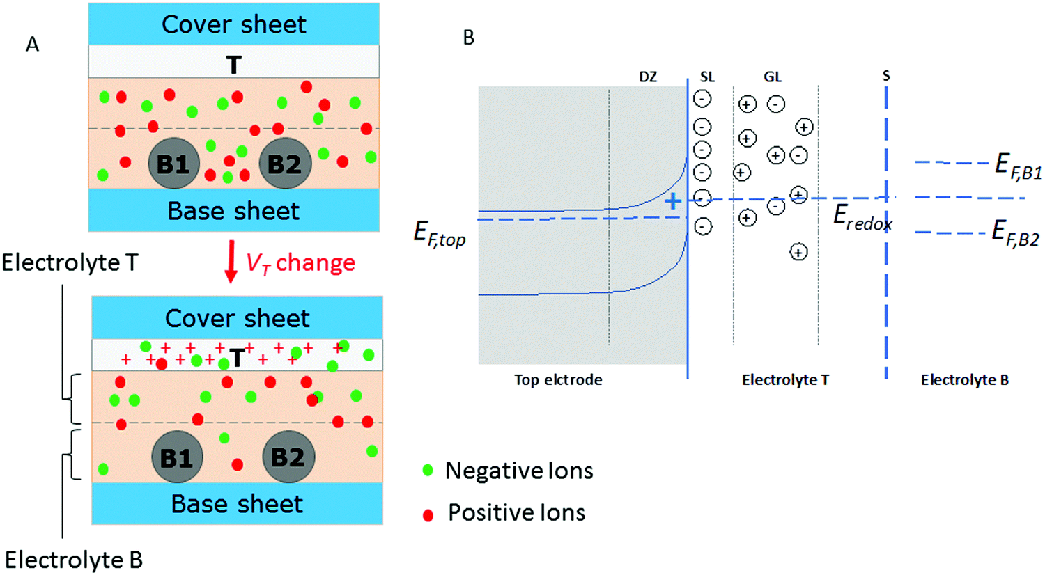 | ||
| Fig. 7 (A) Schematic description of the mechanism of the device. (B) The IVEST energy levels and relevant charge layers. The image shows the electronic depletion zone (DZ), the Stern layer (SL), the Gouy layer (GL), and the separator (S). The left half of Fig. 7B shows the classical description of a semiconductor electrolyte interface as e.g. in ref. 27. The right half shows the proposed coupling to the bottom part of the electrolyte. The Fermi energy offsets are generated by external voltages. | ||
A change in potential would change the depletion layer inducing a change in the ionic adsorption layer. This, in turn, would change the ion concentration in the B-part of the device leading to the resistance change. Since the adsorption/desorption phenomena are nearly current-free, the input current is low whereas the output current mainly depends on the output voltage. So, the output current is normally not low. This fundamental difference of the input and output current is the root of the amplification of the device.
For a quantitative estimation, we use the Mott–Schottky theory.28 In addition, the basic equation for the coupling of the semiconductor with the electrolyte is assumed to be:
| NE = endAwγ | (6) |
| GBB = G0 − α1(Vtop − Vfb)1/2 for Vtop > Vfb | (7) |
 | (8) |
The physical meaning of this formula is very similar to the Mott–Schottky formula. The depletion layer disappears near the flat-band potential; however, it also shows the strongest modifications there. Therefore, the selection of the working point near the flat-band potential seems to be most appropriate. On the other hand, in this region also the conductivity of the interface increases. Therefore, the optimization of the amplification is a delicate balance between increasing the transconductance and keeping the resistance high.
4.2 The potentiometric effect
The basic action of the device can be regarded as a potentiometer with external control voltage. This control voltage has a very nonlinear effect as can be seen from Fig. 4. A part of these effects is instantaneous, and another part can be modified by a waiting time. Therefore, we think that two mechanisms contribute to the effect. The first is the voltage-controlled adsorption of ions in the TiO2 electrode and the second is the ion transport through the membrane. Both mechanisms can change the concentration of ions. The instantaneous effect can be good to construct an amplifier. Using a relatively long writing period, the transport phenomena become dominating.The control current created by the voltage can be seen from Fig. S2 in the ESI.† This Figure also clarifies why a relatively high control voltage was used for the writing phase. Here a significant current is flowing.
The nonlinearity of the control current dependent on the control voltage might be regarded as a useful feature. It creates an in-build threshold switch or, more generally, an activation function in neural networks. The basic potentiometer characteristics in the output are well suited for perceptrons or neuromorphic networks for realizing signal weighting.
4.3 Memory effects and the role of membranes
While trans-conductance phenomena only need instantaneous interactions and nonlinearities for explanation, memory effects are based on multi-stability or non-equilibrium states. For our device, non-equilibrium phenomena seem to be most important. A distinction should be made between the “main memory effect”, i.e. the memory effect which is intended to be used in a device, and other memory effects which only disturb our measurements.The main memory effect found in the IVESTs can likely be explained by the different concentrations of ions between the two parts of the device. The T-part of IVEST is the top electrode and a part of the electrolyte, while the second part of the IVEST consists of two bottom electrodes and the electrolyte surrounding them (“B-part”). When a voltage is applied, gradients of the electrolyte ions are formed in the device creating non-equilibrium states between the two parts of the device. In the readout phase (i.e. without control voltage), the ions need time to redistribute again and to reach an equilibrium state. This time (stability time) is usable for the memory.
Fig. 8 shows a brownish color between and near the two bottom electrodes. We observed this coloration when applying higher voltages (|Vtop| > 0.6 V) on the top electrode. This coloration is a clear indication of I3− or polyiodides accumulated near the two bottom electrodes creating a non-equilibrium state. Very likely, also I3− depletions occur and also the iodide ions form such gradients. The top electrode is expected to play a significant role in the enhancement of the non-equilibrium concentration between the two parts of the device. Fig. 6A shows that by increasing the thickness of TiO2 on the top electrode, Δ2RBB decreases. This effect is a bit counter-intuitive. But one needs to consider that the TiO2 electrodes are not ideal and have an active part and some dead material which is not interconnected to the metal support. This material would explain the negative effect of a thick TiO2 layer.
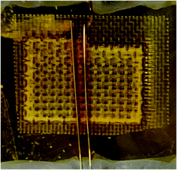 | ||
| Fig. 8 Photo of the coloration of the B-electrodes. | ||
The separator typically used for the construction of the device can be varied in a wide range of pore sizes. For small pore sizes, it acts as a membrane which can slow down the redistribution of ions between the T-part and the B-part of the device. It increases the lifetime of the non-equilibrium state and may, therefore, enhance the memory effect. Such an enhancement can actually be seen in Fig. 6D. Here, decreasing the pore size led to an increase in the stability time τ2. The membrane pore size influenced Δ2RBB and is shown in Fig. 6B. Using a membrane with a smaller pore size increased Δ2RBB by a factor of 5.
Another memory effect becomes visible during variations of the read-out process (i.e. variation of the readout time and used current). There one can find different memory curves. In addition, the coloration of one of the B-electrodes becomes visible. Obviously, redistribution of ions within the B-part occurs. This second memory effect might be useful for special circuit layouts. However in the frame of this work, it is only a disturbance of the characterization measurements.
4.4 Adaptation, stability time of memory states and physical effects
The device has two metastable states HRS and LRS in the readout phase. The meta-stability of each state becomes visible in two kinetic processes with different time constants (Fig. 9). The first one can be called adaptation and is visible within a time of < 2 min. It is characterized by the time constant τ1. Since it occurs directly after the writing process, the gradients created during writing might be responsible for this relatively fast decay.The second visible process during readout has a time constant of τ2 > 2 min and can durate over times up to hours. The constant is called the stability time and determines how long the state can be used for storing information. After this time, the two metastable states are assumed to reach the equilibrium state of the device.
Mathematically, the sum and the difference of the two resistances were fitted to obtain τ2 and ΔRBB in a reliable manner (see the ESI†). Values of Δ2RBB = 0.56 kΩ and τ2 = 5.8 h were obtained indicating a very useful kind of memory. In particular, the τ2-time limits the usability of the memory since after this time a refreshment process is needed to store information for a longer time.
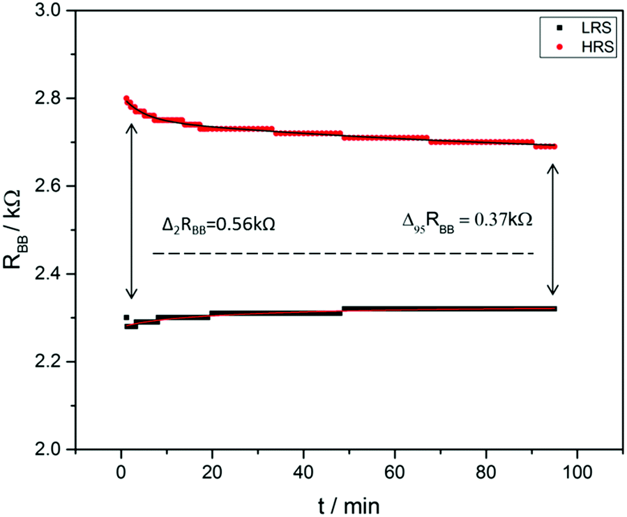 | ||
| Fig. 9 The behavior of the two resistance states over 95 min. The dashed line represents the equilibrium state of the device. The measurement was carried out at an optimized cell (sample 285) with a separator pore size of 1.2 μm, an electrolyte with Xe = 0.16 and a titania layer with XTiO2 = 0.5. | ||
For the interpretation of the dynamical phenomena we use the same physical picture as in Section 4.2 with focus on the redistribution of I2. In particular, the low concentrations will lead to a (variable) depletion of I3− in the B-part. Now one has to consider that the resistance between two electrodes includes different contributions: the two electrode surfaces including the ion layers in the electrolyte and the volume contribution of the electrolyte. Whereas the volume contribution is not strongly dependent on the kind of ion, the electrode contributions are very sensitive. The exchange of I3− with I− has a dramatic effect on the redox reactions and, therefore, on the electrode resistance. For a quantitative estimation of such effects, one can use models as e.g. described in ref. 29.
As said above, the decisive influences can be expected from the extinction of I3− which is the oxidizer part of the redox couple. Therefore, we would like to call the proposed mechanism “redox oxidizer depletion”. In the writing process this depletion is generated or removed mainly between the two cell parts. However in addition, intra-part gradients are formed. In the beginning of the readout process these gradients will decay. We ascribe this to the typical time τ1. Later in the readout phase, the inter-part gradients are of importance only. They lead to the typical decay time τ2. One could now make an estimation on the τ2(dp)-dependence. However, our measured dependence includes not a variation of dP alone, but also of the thickness and kind of material. Therefore, quantitative agreement cannot be expected. In addition to this open point, the investigation of other ionic gradients is still in progress.
5 Conclusions
A new purely ionic soft triode was constructed. It can be used as a memory or an amplifier. Two physico-chemical principles are likely to be realized in the device, ion adsorption in a porous electrode and redox oxidizer depletion. Both principles allow a wide range of chemical tuning. A non-equilibrium of ions occurs between the two parts of the device, which can be used to control the current in the device.Different simple tuning factors were studied. The amplification of the device was optimized and reached a value of β = −52. The memory effect was optimized and reached Δ2RBB = 0.56 kΩ and τ2 = 5.8 h by using a membrane with a pore size of 1.2 μm, an diluted electrolyte (16% of our standard) and a thinner titania layer (of about 10 μm). The high stability time of the device allows it to be used as a memory element in different applications such as sensor systems,30 health care applications31 and neuromorphic memories. This device could be a building block for neuromorphic information processing systems and could, therefore, be a step towards a new computational technology.
The device has several advantages in comparison with known devices such as the possibility of a green fabrication involving no high-temperature step, the possibility of incorporation into printable electronics, and the low power consumption of such devices. It should be underlined that there is no need to use a semi-conductor material to create a channel between the bottom electrodes. This would always increase the production cost. Liquid electrolytes seem to be a drawback, but existing widely used devices as batteries and electrolytic capacitors show that one can well manage the technical requirements. In addition, solid or gel electrolytes can be used for such devices as well.
From the device point of view, it is interesting that the IVESTs have a controllable linear Ohmic output. This is a difference to the known devices, which have strongly non-linear output characteristics. However, this fact enables and enforces modified circuit layouts.
Conflicts of interest
The authors declare no conflict of interest.Acknowledgements
The authors would like to thank U. Petrat and H. Köster for providing support in carrying out the experiments. We thank W. Schmidt for a critical reading of the manuscript. E.M. acknowledges the Erasmus+ program (2016-KA1-Student mobility) of the European Commission for support.References
- J. Leger, M. Berggren and S. Carter, Iontronics: Ionic carriers in organic electronic materials and devices, CRC Press, 2010 Search PubMed.
- L. Hegedus, N. Kirschner, M. Wittmann and Z. Noszticzius, J. Phys. Chem. A, 1998, 102, 6491–6497 CrossRef.
- W. H. Brattain and R. B. Gibney, Three-electrode circuit element utilizing semiconductor materials, US Patent, US2524034A, 1948 Search PubMed.
- R. E. Hetrick, Electrochemical transistor structure with two spaced electrochemical cells, US Patent, 4,332,003, 1984 Search PubMed.
- G. Bruno, G. Canavese, X. Liu, C. S. Filgueira, A. Sacco, D. Demarchi, M. Ferraria and A. Grattoni, Nanoscale, 2016, 8, 18718–18725 RSC.
- S.-W. Nam, M. J. Rooks, K.-B. Kim and S. M. Rossnagel, Nano Lett., 2009, 9, 2044–2048 CrossRef CAS PubMed.
- P. Janson, E. O. Gabrielsson, K. J. Lee, M. Berggren and D. T. Simon, Adv. Mater. Technol., 2019, 4, 1800494 CrossRef.
- K. Tybrandt, K. C. Larsson, A. Richter-Dahlfors and M. Berggren, Proc. Natl. Acad. Sci. U. S. A., 2010, 107, 9929–9932 CrossRef CAS PubMed.
- F. Wang, P. Stepanov, M. Gray, C. N. Lau, M. E. Itkis and R. C. Haddon, Nano Lett., 2015, 15, 5284–5288 CrossRef CAS PubMed.
- M. T. Ghoneim and M. M. Hussain, Electronics, 2015, 4, 424–479 CrossRef CAS.
- R. Waser, R. Dittmann, G. Staikov and K. Szot, Adv. Mater., 2009, 21, 2632–2663 CrossRef CAS.
- E. Madai, B. Matejczyk, A. Dallos, M. Valisko and D. Boda, Phys. Chem. Chem. Phys., 2018, 20, 24156–24167 RSC.
- H. Zhang, C. Cheng, H. Zhang, R. Chen, B. Huang, H. Chen and W. Pei, Phys. Chem. Chem. Phys., 2019, 21, 23758–23763 RSC.
- Y. Shan, Z. Lyu, X. Guan, A. Younis, G. Yuan, J. Wang, S. Lia and T. Wu, Phys. Chem. Chem. Phys., 2018, 20, 23837–23846 RSC.
- W. Zhang, R. Mazzarello, M. Wuttig and E. Ma, Nature, 2019, 4, 150–168 CAS.
- S. Menzel, S. Tappertzhofen, R. Waser and I. Valov, Phys. Chem. Chem. Phys., 2013, 15, 6945–6952 RSC.
- Z. Wang, K. L. Wang, H. Wu, Q. Xia, G. W. Burr, J. J. Yang and C. S. Hwang, Nat. Rev. Mater., 2020, 5, 173–195 CrossRef CAS.
- A. Chen, Solid state electrochemistry II: electrodes, interfaces and ceramic membranes, John Wiley & Sons, 2012 Search PubMed.
- S. O. Abdellatif, S. Josten, A. S. G. Khalil, D. Erni and F. Marlow, IEEE J. Photovolt., 2020, 10, 522–530 Search PubMed.
- F. Marlow, A. Hullermann and L. Messmer, Adv. Mater., 2015, 27, 2447–2452 CrossRef CAS PubMed.
- P. Horowitz and W. Hill, The Art of Electronics, Cambridge Univ. Press, 1989 Search PubMed.
- S. Abdellatif, P. Sharifi, K. Kirah, R. Ghannam, A. S. G. Khalil, D. Erni and F. Marlow, Microporous Mesoporous Mater., 2018, 264, 84–91 CrossRef CAS.
- P. R. F. Barnes, K. Miettunen, X. Li, A. Y. Anderson, T. Bessho, M. Grätzel and B. C. O’Regan, Adv. Mater., 2013, 25, 1881–1922 CrossRef CAS PubMed.
- K. Tybrandt, E. O. Gabrielsson and M. Berggren, J. Am. Chem. Soc., 2011, 133, 10141–10145 CrossRef CAS PubMed.
- H. Yuan, H. Shimotani, A. Tsukazaki, A. Ohtomo, M. Kawasaki and Y. Iwasa, Adv. Funct. Mater., 2009, 19, 1046–1053 CrossRef CAS.
- L. Herlogsson, X. Crispin, N. D. Robinson, M. Sandberg, O.-J. Hagel, G. Gustafsson and M. Berggren, Adv. Mater., 2007, 19, 97–101 CrossRef CAS.
- X. G. Zhang, Electrochemistry of Silicon and its Oxide, Springer, 2007 Search PubMed.
- A. J. Bard and L. R. Faulkner, Electrochemical Methods: Fundamentals and Applications, Wiley, New York, 1980 Search PubMed.
- J. Akilavasan and F. Marlow, J. Phys. Chem. C, 2020, 124, 4101–4108 CrossRef CAS.
- A. Chhetry, J. Kim, H. Yoon and J. Y. Park, ACS Appl. Mater. Interfaces, 2018, 11, 3438–3449 CrossRef PubMed.
- B. Nie, R. Li, J. Cao, J. D. Brandt and T. Pan, Adv. Mater., 2015, 27, 6055–6062 CrossRef CAS PubMed.
Footnote |
| † Electronic supplementary information (ESI) available. See DOI: 10.1039/d1cp04581d |
| This journal is © the Owner Societies 2022 |