
 Open Access Article
 This Open Access Article is licensed under a Creative Commons Attribution-Non Commercial 3.0 Unported Licence
Physical and chemical aspects at the interface and in the bulk of CuInSe2-based thin-film photovoltaics
Shogo
Ishizuka
 *a,
Jiro
Nishinaga
a,
Kosuke
Beppu
b,
Tsuyoshi
Maeda
b,
Fuuka
Aoyagi
b,
Takahiro
Wada
b,
Akira
Yamada
c,
Jakapan
Chantana
d,
Takahito
Nishimura
d,
Takashi
Minemoto
d,
Muhammad Monirul
Islam
e,
Takeaki
Sakurai
e and
Norio
Terada
f
*a,
Jiro
Nishinaga
a,
Kosuke
Beppu
b,
Tsuyoshi
Maeda
b,
Fuuka
Aoyagi
b,
Takahiro
Wada
b,
Akira
Yamada
c,
Jakapan
Chantana
d,
Takahito
Nishimura
d,
Takashi
Minemoto
d,
Muhammad Monirul
Islam
e,
Takeaki
Sakurai
e and
Norio
Terada
f
aNational Institute of Advanced Industrial Science and Technology, Umezono, Tsukuba, Ibaraki, Japan. E-mail: shogo-ishizuka@aist.go.jp
bRyukoku University, Seta, Otsu, Shiga, Japan
cTokyo Institute of Technology, Ookayama, Meguro-ku, Tokyo, Japan
dRitsumeikan University, Noji-higashi, Kusatsu, Shiga, Japan
eUniversity of Tsukuba, Tennodai, Tsukuba, Ibaraki, Japan
fKagoshima University, Korimoto, Kagoshima, Japan
First published on 22nd December 2021
Abstract
Chalcopyrite CuInSe2 (CISe)-based thin-film photovoltaic solar cells have been attracting attention since the 1970s. The technologies of CISe-based thin-film growth and device fabrication processes have already been put into practical applications and today commercial products are available. Nevertheless, there are numerous poorly understood areas in the physical and chemical aspects of the underlying materials science and interfacial and bulk defect physics in CISe-based thin-films and devices for further developments. In this paper, current issues in physical and chemical studies of CISe-based materials and devices are reviewed. Correlations between Cu-deficient phases and the effects of alkali-metals, applications to lightweight and flexible solar minimodules, single-crystalline epitaxial Cu(In,Ga)Se2 films and devices, differences between Cu(In,Ga)Se2 and Ag(In,Ga)Se2 materials, wide-gap CuGaSe2 films and devices, all-dry processed CISe-based solar cells with high photovoltaic efficiencies, and also fundamental studies on open circuit voltage loss analysis and the energy band structure at the interface are among the main areas of discussion in this review.
 Shogo Ishizuka, Jiro Nishinaga, Kosuke Beppu, Tsuyoshi Maeda, Fuuka Aoyagi, Takahiro Wada, Akira Yamada, Jakapan Chantana, Takahito Nishimura, Takashi Minemoto, Muhammad Monirul Islam, Takeaki Sakurai, and Norio Terada (from upper-left in the order of authorship) | Shogo Ishizuka investigates CuInSe2-based energy conversion materials and devices at the National Institute of Advanced Industrial Science and Technology (AIST). |
Jiro Nishinaga is a senior researcher at AIST investigating epitaxial growth of Cu(In,Ga)Se2 thin films. |
Kosuke Beppu is an assistant professor at Ryukoku University and investigates the local structure around constituent atoms in CuInSe2-based materials using XAFS. |
Tsuyoshi Maeda is a researcher at Ryukoku University and investigates electronic structures of CuInSe2 and related materials using first principles calculation. |
Fuuka Aoyagi is a graduate student at Ryukoku University under the supervision of Prof. Wada. |
Prof. Takahiro Wada is a professor at Ryukoku University and studies ternary and multinary compounds such as chalcopyrite-type CuInSe2. |
Prof. Akira Yamada (Dr Eng) is professor at Tokyo Institute of Technology developing Cu(In,Ga)(S,Se)2 thin-film solar cells. |
Prof. Jakapan Chantana (PhD) is professor at Ritsumeikan University working on fabrication and characterization of compound semiconductor thin-film solar cells. |
Takahito Nishimura is assistant professor at the Ritsumeikan Global Innovation Research Organization, Ritsumeikan University, working on the development of compound solar cells. |
Prof. Takashi Minemoto is professor at Ritsumeikan University working on fabrication and characterization of compound semiconductor thin-film solar cells. |
Muhammad Monirul Islam is assistant professor at University of Tsukuba working on energy conversion materials for application in solar cells, photocatalytic devices, and batteries. |
Prof. Takeaki Sakurai is professor at University of Tsukuba working on characterization of optical semiconductor devices. |
Prof. Norio Terada is professor at Kagoshima University working on characterization of electronic structure of electronic materials and devices. |
1 Introduction
CuInSe2 (CISe)-based photovoltaic solar cells1–3 and modules,4,5 which are now manufactured using multinary compounds consisting of a wide variety of elements based on the I–III–VI2 material system (I, III, and VI are group I, III, and VI elements, respectively) such as (Ag,Cu)(In,Ga)(S,Se)2, have demonstrated photovoltaic efficiencies of as high as 23.35% from small area cells6 and about 20% from modules.7,8 Today, Si wafer-based technologies are dominant in the photovoltaic solar module market. Nonetheless, thin-film technologies which include CISe-, CdTe-, and perovskite-based solar cells are promising because they are expected to cover new photovoltaic module markets, which are different from those of conventional Si-based modules. For example, lightweight and flexible photovoltaic modules and applications to highly efficient and cost-effective tandem solar cells and modules are among their bright possibilities.Among thin-film photovoltaic technologies, CISe-based compounds, with band-gap energy (Eg) values controllable in a relatively wide range from, for example, 1.0 eV (CISe) to 2.4 eV (CuGaS2) by alloying, are attractive in terms of high absorption coefficients that allow the photoabsorber layer to be thinner than several micrometers, good durability for irradiation, relatively short energy payback time, and small carbon footprint of the products.9
Physical and chemical aspects of CISe-based multinary compound thin-films and photovoltaic devices are relatively complicated when compared with “orthodox” semiconducting materials such as Si and GaAs and thus a multitude of poorly understood areas remain. Also, CISe-based film properties often depend on growth methods such as selenization/sulfurization of metal precursors and coevaporation and growth conditions.10 An ongoing and deep study on CISe-based films and devices is, therefore, essential and is expected to lead to further developments which enhance energy conversion efficiencies as well as deepening the understanding of the underlying physics and chemistry. In this article, recent studies on physical and chemical aspects of the surface, interface, and bulk of CISe-based thin-films and devices are reviewed. It is thought that reduction of carrier recombination at the interface and in the bulk CISe-based films and devices is key to enhancing solar cell parameter values such as open circuit voltage (VOC) and fill factor (FF), and thus photovoltaic efficiency. Here, technical developments required to achieve this are discussed. In Section 2, control of alkali-metal doping and the properties of surface Cu-deficient layer (CDL) are discussed. Progress of monolithically integrated lightweight and flexible Cu(In,Ga)Se2 (CIGSe) minimodules is reported to exemplify CISe-based photovoltaic technologies. In Section 3, the characteristics of materials and devices are comparatively studied using single-crystalline epitaxial CIGSe films and conventional polycrystalline CIGSe films. Crystallization of Cu- and Ag-based chalcopyrite materials and thin-film growth of CuGaSe2 (CGSe) are discussed in Sections 4 and 5, respectively. In Section 6, efficiency enhancements in Cu(In,Ga)(S,Se)2 (CIGSSe) solar cells fabricated using an all-dry process are considered. In Section 7, an analysis of open circuit voltage loss with carrier recombination is discussed. In Section 8, depth-directional profiles of electronic structure of CdS buffer/CIGSSe absorber structure in high performance cells as determined by direct and inverse photoelectron spectroscopy are summarized.
2 Role of Cu-deficient Cu(In,Ga)Se2 thin-film surface
2.1 Effects of alkali-metal halide postdeposition treatment
Alkali-metal doping is one of the most critical factors required to boost CISe-based photovoltaic device performance. After the initial report of alkali-metal beneficial effects on CISe devices in the early 1990s,11 a wide variety of alkali-metal doping control methods have been attempted in addition to the use of alkali-containing glass substrates. Those include techniques such as NaF or other alkali-halide precursor deposition on a Mo back contact layer,12,13 the use of MoNa compound back contacts14,15 or a sputtered soda-lime glass thin-layer on the substrate prior to Mo back contact deposition,16,17 and postdeposition treatment (PDT).18 In particular, PDT using relatively heavy alkali-metal halides such as KF, RbF, and CsF have led to significant efficiency enhancements in CISe-based photovoltaic devices.6,19,20 Today, PDT is one of the most promising alkali-metal doping control techniques. In addition to the effects of alkali-metals diffused from the substrate side, PDT methods using relatively heavy alkali-metals likely modify the film surface (device interface) resulting in a decrease in carrier recombination in the interface region leading to enhanced photovoltaic performance.21–23 The mechanism behind the PDT effects may include the formation of alkali-metal compound phases such as KInSe2 and RbInSe2 at the interface.24–26 The effects of PDT are, however, often dependent on the alkali-metal species used and CISe-based film properties such as elemental composition and surface conditions. This fact leads to both improvement and degradation of device performance with PDT for different experimental conditions.27,28The beneficial effects of the lightest alkali-metal Li doping in CIGSe films and devices are negligible when compared to the effects obtained with heavier alkali-metals Na, K, Rb and Cs.29 The effects of Na was historically the most studied among these alkali-metals and the beneficial effect enhancing photovoltaic performance has been proven.11–18 Elemental K and heavier elements are similarly effective and the effect of elemental Rb has been suggested to be particularly significant,30 although the highest photovoltaic efficiency reported to date has been achieved with Cs treatment of a CIGSSe photoabsorber layer.6 To obtain beneficial effects with PDT, it has been suggested that the control of Cu-deficient phases present on the CIGSe film surface and the amount of alkali-halide supply appropriate to the surface condition are key.31 Typically CIGSe films grown by the three-stage coevaporation process32 possess a Cu-deficient surface, although the degree of Cu-deficiency as indicated by the [Cu]/([Ga] + [In]) (CGI) and group III elemental composition ([Ga]/([Ga] + [In])) (GGI) and their fluctuations may depend on CISe-based films prepared in each laboratory. For the case of RbF-PDT, the presence of a CDL on the CIGSe film surface was found to significantly affect the results of PDT and lead to variations in the photovoltaic device parameters and consequent photovoltaic performance.31 For example, Fig. 1 shows the photovoltaic parameter variations observed with RbF-PDT performed on CIGSe films grown with a very thin (nominally 0 nm) and a thick (approximately 500 nm) high In-content (GGI < 0.03) CDL surface.31 Decreases in the open circuit voltage (VOC), fill factor (FF), and concomitant photovoltaic solar cell efficiency values were observed with increasing the CDL thickness (blue boxes), which were similar to the results reported in the literature.33,34 These values improved with RbF-PDT when the CDL thickness was thick enough, whereas the device performance was found to degrade with RbF-PDT when the CDL was absent or very thin (red boxes). A similar trend could be observed for KF-PDT in the literature.27 It was found that RbF-PDT performed on a CIGSe film fabricated without a surface CDL led to an increase in interfacial recombination.31 These results suggest that an appropriate thick CDL is necessary to obtain beneficial effects with PDT to modify the device interface properly.
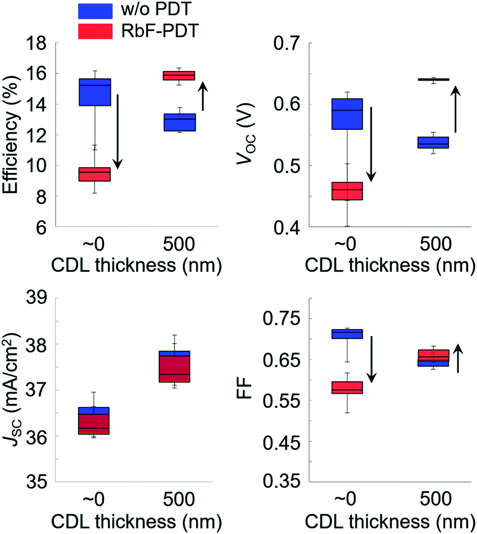 | ||
| Fig. 1 Solar cell parameter variation trends obtained with RbF-PDT performed on thin (∼0 nm) and thick (500 nm) CDL-surface CIGSe film devices grown on SLG substrates. The arrows indicate variational trends with RbF-PDT. JSC; short circuit current density. | ||
A CDL, consisting of Cu-deficient phases such as CuIn3Se5, is expected to play a role of a hole barrier at the CuInSe2/CDL/CdS interface35 resulting in a decrease in carrier recombination in the interface region. In addition to this, a CDL is suggested to play an important role of controlling the alkali-metal beneficial effects in CISe-based devices. Alkali-metals (except for Li) tend to concentrate in the CDL present on the film surface regardless of diffusion from the substrate side (alkali-metal supply from the back side) or PDT (supply from the surface side).17,29,36 In other words, Cu-deficient phases can be a reservoir of alkali-metals. Alkali-metals incorporated in a CDL are expected to lead to changes in the interfacial energy band structure,21,37–39 although there is room for further discussion about the detailed mechanisms behind alkali-metal effects in CISe-based films and devices, namely, the effects of alkali-metals present in the bulk and at grain boundaries in the film and their differences.
The effects of CDL present on the film surface and at grain boundaries should be separately discussed. Nevertheless, CDL is likely to serve as a hole barrier at the surface and grain boundaries as mentioned above. This is due to the fact that Cu-deficient phases have a wider band-gap energy (Eg), for example, the Eg of CuInSe2 and CuIn3Se5 are 1.0 eV and 1.2–1.3 eV, respectively,35,40 and the valence band maximum (VBM) is determined by the Cu 3d and Se 4p antibonding states, and thus Cu-deficiency leads to lowering the VBM. The effects of CDL on variations in the conduction band minimum (CBM) still remain unclear. For the case of the film surface, a model which suggests that the CDL lowers the CBM as well as VBM, and thus enhancements in the formation of a “cliff” interface is a consensus in the literature,35,41,42 and a schematic is shown in Fig. 2a. On the other hand, some different models have been suggested for the case of the grain boundaries present in CISe-based films. In addition to the model of lowering CBM, flat and upward bending models of the CBM as shown in Fig. 2b have been also suggested.43–47 Such a CBM structure is effective at repelling electrons, which are the minority carriers in the CISe-based film, from grain boundaries. Note that the energy band diagram at the grain boundaries may vary with CGI and GGI compositional fluctuations and the presence of alkali-metals.48,49 Alkali-metals have been suggested to be effective reducing the potential fluctuation resulting in enhanced VOC, FF and concomitant photovoltaic efficiency.49 In all models, the presence of alkali-metals is expected to modify the energy band structure of the CDL and contribute to a reduction of carrier recombination at the interfaces. The carrier transport in polycrystalline CISe-based films should be discussed on the basis of a three-dimensional (3D) structure. Once downward bending of VBM is present, it repels holes from the grain boundary, leading to a reduction in the recombination rate at the grain boundary even if electrons drift towards grain boundaries, due to the electric field in the CIGSe layer perpendicular to the substrate.43
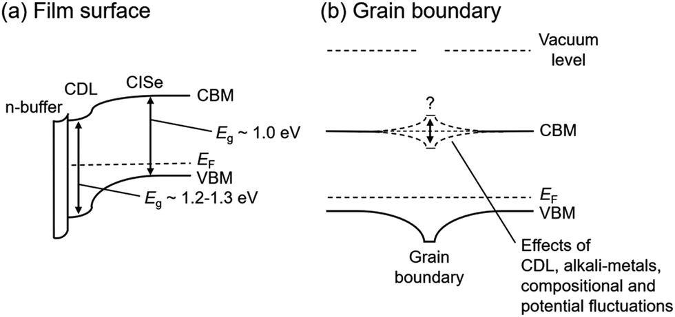 | ||
| Fig. 2 Schematic energy band diagram models (a) around the CISe-based film surface and (b) grain boundary in the film proposed to date. The CBM of the CDL shown in (a) may also vary with the presence of alkali-metals and compositional fluctuations. | ||
Further investigation on the grain boundary physics and chemistry is necessary to develop polycrystalline CISe-based thin-film photovoltaic technologies. Therefore, more sophisticated and detailed characterizations are desired. Changes in the local composition and alkali-metal distribution profiles which may occur during measurements are also important issues which should be concerned. In fact, we have observed elemental Cu accumulation occurring at CIGSe grain boundaries during transmission electron microscopy (TEM)-energy dispersive X-ray spectroscopy (EDX) measurements using an electron probe with an acceleration voltage of 300 kV.50 This kind of observationally induced compositional change may lead to the misleading conclusion that there is Cu-rich composition at the grain boundary. Thus, the combined use of several measurement techniques, for example, TEM-EDX for good spatial resolution (∼0.2 nm), secondary ion mass spectrometry (SIMS) for a good detection limit (∼1 ppb), and in some cases atom-probe tomography (APT) for a 3D elemental image mapping, is ideal to obtain multiple and reliable information from complicated CISe-based thin-film materials and devices.
2.2 Alkali-metal doping control on alkali-free flexible substrates
The most flexible substrate materials, which include metal foils, polyimide films, and ceramic sheets, used for lightweight and flexible/bendable CISe-based photovoltaic module fabrication, contain no alkali-metals unlike conventional soda-lime glass (SLG) substrates. PDT techniques are promising to control alkali-metal doping of CISe-based films grown on this type of substrates,19,51 although the handling of heavy alkali-metal halides such as RbF often requires attention due to humidity-induced degradation. The use of stable alkali-metal compounds such as a sputtered soda-lime glass (SLG) thin-layer deposited prior to the Mo back contact layer formation is, therefore, an additional option to realize the precise alkali-metal doping control.16 SLG is an alkali-silicate consisting mainly of Na2O·CaO·5SiO2 with other metal-oxides K2O, Al2O3, and MgO. It is well known that diffusion of alkali-metals Na and K from SLG through the Mo back contact layer into the CIGSe-based film occurs when SLG is used as a substrate. Interestingly, diffusion of other impurities Ca, Al and Mg could be blocked by the Mo layer and thus these impurities did not diffuse into the CISe-based film.52 Furthermore, the Na and K concentration in CISe-based films is controllable with the thickness of sputtered SLG thin-films deposited on alkali-free substrates such as metal foils.17 This fact enables precise control of Na- and K-doping in CIGSe-based films using SLG thin-films, namely sputtered alkali-silicate thin-layer (ASTL).Unlike the case for PDT, alkali-metal diffusion from the substrate side during film growth affects the structural property of CISe-based films such as crystal growth orientation and grain size.11,12,17,18 Nonetheless, variations in the electrical properties such as an increase in the hole carrier density can be obtained similarly to PDT. Also, the presence of alkali-metals during film growth is expected to modify the bulk crystal quality of CIGSe grains, though most alkali-metals are believed to concentrate at grain boundaries rather than in the bulk.53,54 Differences observed for the alkali-metal effects obtained with different alkali-metal doping techniques with various kinds of alkali-metal species are, therefore, worthy of further investigation.
The combination of alkali-metal (mainly Na and K) diffusion from the ASTL deposited prior to the sputtering of the Mo back contact layer and PDT using RbF enables precise control of the bulk and surface properties of CISe-based films. To date, a 18.64%-efficient (VOC ∼ 12.7 V (0.747 V per cell), JSC ∼ 34.6 mA cm−2, and FF ∼ 72.0%) 17-cell monolithically integrated CIGSe solar minimodule has been demonstrated on an alkali-free flexible substrate using a combination of alkali-metal doping control techniques (Fig. 3).55 The minimodule structure and the fabrication process can be found elsewhere.55 The result obtained and this kind of approaches are expected to open a new frontier of a wide variety of applications of CISe-based photovoltaic technologies.
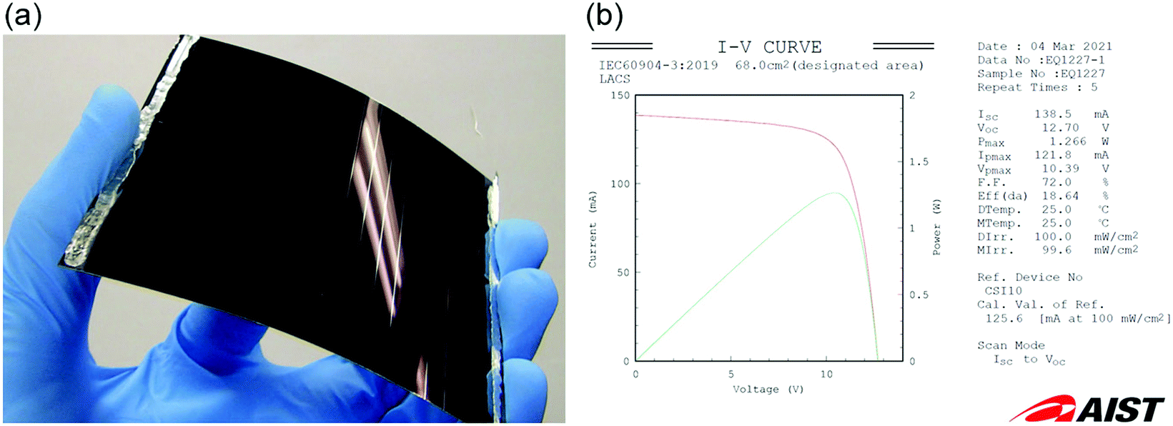 | ||
| Fig. 3 (a) A 18.64%-efficient flexible CIGSe solar minimodule and (b) the corresponding data sheet of the independently certified current–voltage (red line) and power-voltage (green line) curves. | ||
3 Crystalline properties of epitaxial Cu(In,Ga)Se2 solar cells
CIGSe solar cells generally used are based on polycrystalline thin-films deposited on SLG or flexible substrates by codeposition or selenization of metal precursors. It is often complicated to analyze the device physics in detail due to the presence of many grain boundaries and crystal defects. Epitaxial CIGSe layers without grain boundaries have the potential to increase the photovoltaic efficiency, and layers with high crystalline quality are an ideal structure for fundamental research. Many researchers have tried achieving such potentially high photovoltaic efficiency using epitaxial CIGSe layers.56–60 For example, Niki et al. grew epitaxial CuInSe2 (CISe) layers on GaAs substrates using codeposition at growth temperatures in the range of 350–550 °C. The CISe films were grown on a pseudo-lattice-matched InGaAs layer on GaAs(001) substrates, and the authors concluded that a reduction in the mismatch strain enabled the growth of high-quality CISe epitaxial films.57 Fujita et al. investigated the epitaxial growth of CuGaSe2 (CGSe) on GaAs(001) substrates with several Cu compositions. Under Cu-rich growth conditions, segregation of Cu2Se on CGSe was observed, and there was a high density of voids between the CGSe layers and GaAs substrates because the Ga atoms in GaAs were drawn out by excess Cu atoms.59 These reports are important for understanding the growth mechanism of highly crystalline CIGSe layers; however, there are few reports of epitaxial CIGSe solar cells with high photovoltaic efficiencies. Recently, we demonstrated photovoltaic efficiencies of over 20% using epitaxial CIGSe layers using techniques developed for high-efficiency polycrystalline CIGSe solar cells.61,62 Ga grading, NaF doping, KF postdeposition treatment (KF-PDT), and heat light soaking (HLS) have been shown to be effective methods to improve the photovoltaic efficiencies of epitaxial CIGSe absorbers as well as polycrystalline absorber layers. In this chapter, we show the crystalline properties of epitaxial CIGSe layers grown on GaAs substrates using the three-stage process and codeposition (Cu, In, Ga, and Se). Many dislocations and voids are present in the epitaxial CIGS layers grown by the three-stage process. On the other hand, epitaxial CIGS layers with high crystalline quality were achieved using codeposition with high growth temperatures.3.1 Crystalline properties of epitaxial Cu(In,Ga)Se2 layers grown by the three-stage process and codeposition
First, we discuss epitaxial CIGSe layers grown by a three-stage process. Fig. 4 shows the structure of an epitaxial CIGSe solar cell grown on a GaAs (001) substrate. GaAs (001) p+-type substrates were etched using an alkaline etchant, and the oxide layer on the substrate surface was removed by thermal annealing at 560 °C in molecular beam epitaxy (MBE) chamber. After surface cleaning, an epitaxial CIGSe layer was grown by the three-stage process. The growth temperature of the first stage (In, Ga, and Se deposition) was 350 °C, while that of the second (Cu and Se deposition) and third stages (In, Ga, and Se deposition) was 550 °C. The surface structure of the substrate and CIGSe films were investigated by Reflection high-energy electron diffraction (RHEED). The CIGSe surface was observed by scanning electron microscopy (SEM), and bright-field scanning transmission electron microscopy (BF-STEM) was used to investigate the crystalline quality of the CIGSe layers.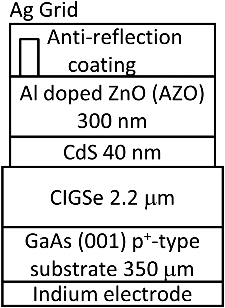 | ||
| Fig. 4 Layer structure of an epitaxial CIGSe solar cell on a GaAs (001) p+-type substrate. | ||
RHEED showed clear double streak patterns from the GaAs surface after thermal cleaning. During the first stage (In, Ga, and Se deposition), RHEED patterns showed 4-fold symmetry characteristic like the GaAs(001) surface, and the patterns showed chevron patterns (not shown here), indicating that {111} facets were formed on InGaSe surface. Fig. 5a shows SEM and BF-STEM images of epitaxial CIGSe layers on GaAs substrate grown by the three-stage process. Uniform facets appeared on the CIGSe surface as can be seen in the SEM image, and the facets were identified to be {112}B of CIGSe crystal. In the BF-STEM image, many dislocations and voids were observed in the CIGSe layer. Large voids appeared in particular at the CIGSe/GaAs interface. At the end of the second stage, Cu2Se segregation occurred in the CIGSe layers due to the presence of Cu-rich conditions, and the Cu2Se compound is likely to react with the GaAs substrate. Then, Ga atoms diffused out from the GaAs substrate leading to the formation of voids at the interface.63 Therefore, it was difficult to fabricate high crystalline quality CIGSe layers with sharp interfaces between CIGSe and GaAs by the three-stage process.
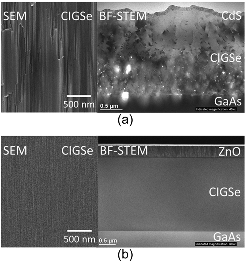 | ||
| Fig. 5 (a) SEM and BF-STEM images of a CIGSe solar cell fabricated by three-stage process. (b) SEM and BF-STEM images of a CIGSe solar cell fabricated by codeposition (Cu, In, Ga, and Se) at 540 °C. | ||
Next, we demonstrate CIGSe epitaxial growth by codeposition (Cu, Ga, In and Se) using high substrate temperatures. After removing the oxide layer from the GaAs surface, an epitaxial CIGSe layer was grown by codeposition at 540 °C. The atomic ratio of Ga to group III elements, GGI, was varied by controlling the flux ratio of In and Ga as previously reported.61,62 Ga grading was introduced by multi-layer depositions with different GGI. The atomic ratio of Cu to group III elements, CGI, was fixed at 0.9 and the CGI of the layers were measured using an electron probe microanalyzer. Sodium ions were incorporated by the codeposition of NaF during CIGSe epitaxial growth, and KF-PDT with Se flux was performed at a substrate temperature of 350 °C after CIGSe layer deposition. A CdS layer was formed by chemical bath deposition. An n-type Al-doped ZnO (AZO) layer was deposited by facing-target DC magnetron sputtering deposition. A silver/chrome electrode was deposited on the AZO layer by evaporation, and the devices were isolated by cleaving.
Fig. 5b shows SEM and BF-STEM images of an epitaxial CIGSe layer on a GaAs substrate grown by codeposition. RHEED patterns showed streak patterns during the CIGSe layer deposition (not shown here), and the surface reconstruction of epitaxial CIGSe layers changed after KF-PDT, and the streak patterns with 4-fold structures changed to double streak patterns. KF-PDT synthesized potassium compounds, such as KInSe2, on the CIGSe surface, as shown in a previous study.61,62 In the BF-STEM image, a single crystal structure without dislocations was observed. No voids and a sharp interface could be observed at the heterointerface between the CIGSe and the GaAs substrates, and lattice images without dislocations were also observed (not shown here). Therefore, the epitaxial relationship between CIGSe and GaAs was fairly good.
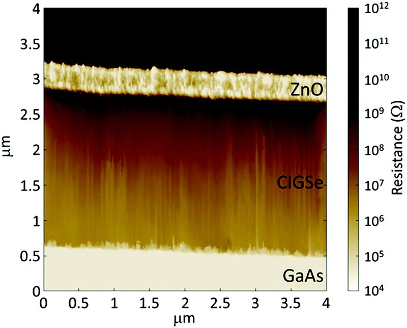
Fig. 6 shows a cross-sectional scanning spreading resistance microscopy (SSRM) image of a high-efficiency CIGSe solar cell grown on a GaAs(001) substrate. SSRM has been an analytical technique used to map the 2D surface carrier distribution in semiconductor devices. In this technique, the local resistivity of a surface can be derived from the electrical current flowing between a conducting atomic force microscope tip and a device surface that is biased relative to it. In Fig. 6, an AZO layer and a GaAs(001) p+-type substrate had low resistance due to high carrier concentrations. However, a dark contrast of resistance was obtained at the surface region of the CIGSe layer, suggesting that a uniform depletion layer of CdS/CIGSe junction appeared in the CIGSe layer.
 | ||
| Fig. 6 Cross-sectional SSRM image of a CIGSe solar cell grown on a GaAs (001) substrate. | ||
Next, we discuss solar cell parameters of the epitaxial CIGSe solar cells. Fig. 7 shows current density–voltage (J–V) curves of epitaxial CIGSe solar cells grown by the three-stage process and codeposition. The photovoltaic efficiency was around 11% for the epitaxial CIGSe solar cells grown by a three-stage process. In contrast, the efficiency achieved was 21% for the epitaxial CIGSe solar cells fabricated by codeposition method. The open circuit voltage was 0.75 V, and the short circuit current density was 35 mA cm−2. The fill factor was 0.81. The carrier concentration was 1 × 1017 cm−3 after heat-light soaking. Ga grading, NaF doping, KF-PDT, and heat light soaking could improve the efficiency of epitaxial CIGSe solar cells, as it does for polycrystalline CIGSe solar cells on SLG substrates.
 | ||
| Fig. 7 J–V curves of epitaxial CIGSe solar cells grown by the three-stage process and codeposition. | ||
4 Migration of constituent atoms in Cu(In,Ga)Se2 and Ag(In,Ga)Se2
We previously studied the migration of constituent atoms, Cu and In, in Cu-poor CuInSe2 (CISe) and Cu and Ga in CuGaSe2 (CGSe) by first-principles calculations with the generalized gradient approximation (GGA).64,65 The activation energies and migration pathways were obtained by means of a combination of linear and quadratic synchronous transit (LST/QST) methods and nudged elastic band (NEB) method. In this study, migration of Cu, In, and Ga in Cu-poor Cu(In,Ga)Se2 (CIGSe) and Ag, In, and Ga in Ag-poor Ag(In,Ga)Se2 (AIGSe) were investigated by similar first-principles calculations in order to understand the diffusion of constituent atoms in CIGSe and AIGSe thin films. The activation energies of Cu migration in CIGSe and Ag migration in AIGSe were discussed on the basis of their pathways.4.1 Theoretical calculation of atomic migration in Cu(In,Ga)Se2
The activation energies of Cu, In, and Ga migration in Cu-poor CIGSe with CGI ratio of 15/16 are shown in Fig. 8a. For all GGI ratios, the activation energy of Cu migration is the smallest while that of In is smaller than that of Ga. These trends are consistent with our previous studies64,65 and experimental results.66 The Cu migration is discussed on the basis of the interactions between migrating Cu atoms and neighboring Se atoms. The variation of the energy during Cu migration in CIGSe is dependent on the interatomic distances between the migrating Cu atom and the neighboring Se atoms.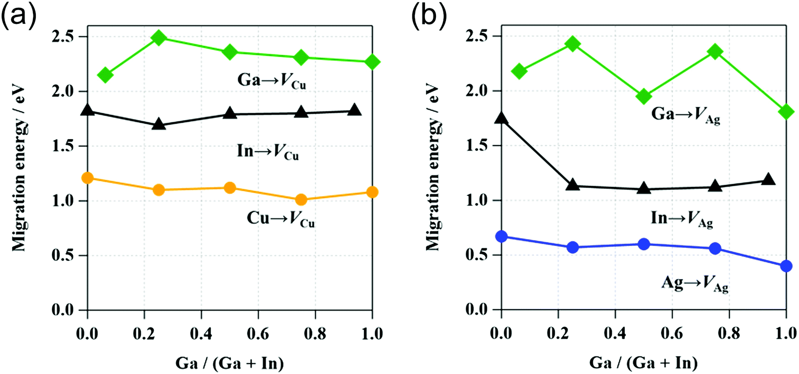 | ||
| Fig. 8 (a) Activation energies of Cu, In, and Ga migration in Cu-poor Cu(GaxIn1−x)Se2 with CGI ∼ 15/16 and (b) those of Ag, In, and Ga migration in Ag-poor Ag(GaxIn1−x)Se2 with [Ag]/([Ga] + [In]) ∼ 15/16. | ||
Fig. 9a shows the variation in the interatomic distances between the migrating Cu atom and the neighboring Se atoms in CISe along the migration pathway. The Se atoms around the diffusing Cu atom are numbered from 1 to 8. In the initial state, Cu is tetrahedrally surrounded by four Se atoms, Se(1), Se(2), Se(3), and Se(4) and in the final state, Cu is also tetrahedrally surrounded by four Se atoms, Se(4), Se(6), Se(7), and Se(8). The initial and final Cu–Se bond lengths (2.425 Å) are in good agreement with the sum of covalent radii of Cu (1.271 Å) and Se (1.145 Å).67 The variations of interatomic distances symmetrically change on both sides of the transition state (the path coordinate corresponds to 0.5 in Fig. 9a). At an early stage of Cu migration (path coordinate of 0.2), Cu atom breaks its chemical bond with Se(1) and then the Cu atom passes near the center of the triangle (one face of the tetrahedron) formed by three Se atoms, Se(2), Se(3), and Se(4). The interatomic distances of Cu–Se(2), Cu–Se(3) and Cu–Se(4) bonds are a little shorter than the initial Cu–Se bond. It is well known that the bond distance between adjacent atoms decreases with decreasing coordination number.68 Near the transition state, the inter-atomic distances of Cu–Se(2) and Cu–Se(3) become longer and those of Cu–Se(6) and Cu–Se(7) become shorter. In the transition state, the diffusing Cu atom passes through the coordinate positions (0.420, 0.625, 0.625) that is offset in the x-axis direction from the octahedral site (center of octahedron) of Se atoms (0.359, 0.624, 0.626). At the transition state, the Cu atom is surrounded by five Se atoms, Se(2), Se(3), Se(4), Se(6), and Se(7). The Cu–Se(4) bond is shorter than the initial Cu–Se bond and the other four Cu–Se bonds are longer the initial Cu–Se bond and shorter than the sum of van der Waals radii of Cu (1.40 Å) and Se (1.90 Å). Although the Cu atom approaches the Se(5) atom, their interaction is small, because the interatomic distance of Cu and Se(5) is considerably longer than the sum of their van der Waals radii. The Cu atom diffuses via Cu vacancies by rotating around the Se(4) atom while maintaining a chemical bond with Se(4).
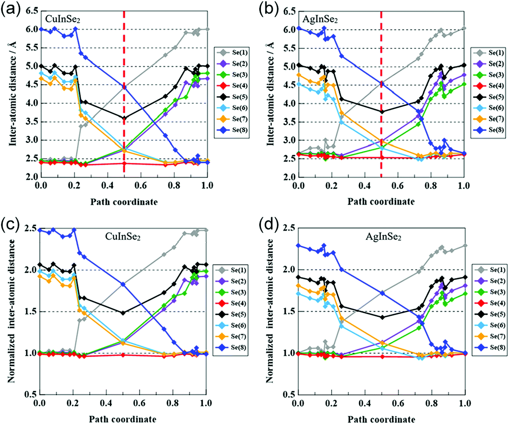 | ||
| Fig. 9 (a) Variations in the calculated interatomic distances between a migrating Cu atom and the neighboring Se atoms in CuInSe2 and (b) those between a migrating Ag atom and the neighboring Se atoms in AgInSe2 along the migration pathway. (c and d) Normalized interatomic distances obtained from the plots in (a and b). | ||
4.2 Interpretation of atomic migration in Cu(In,Ga)Se2
The migration of atoms in CIGSe and AIGSe is significantly associated with the variation of potential energy due to the change of interatomic distance. As shown in Fig. 10a, a parabola can be used as a simple model to describe the relationship between the interatomic distance, r, of two atoms and the potential energy, U. The Morse potential, which is a convenient interatomic interaction model for the potential energy of two atoms, is also shown in the figure. Fig. 10b shows the schematic potential energy of the migrating atom along the migration pathway. The path coordinates of 0.0 and 1.0 correspond the initial and final states, respectively, and that of 0.5 corresponds the transition state. We studied diffusion properties of the constituent atoms in CIGSe by X-ray absorption fine structure (XAFS).69 The XAFS provides the element specific local structure, which includes the interatomic distance between the target element and the neighboring atoms and Debye–Waller factor representing vibration of chemical bond between the target element and the neighboring atom. The chemical bond is analyzed by assuming a harmonic oscillator (Einstein model). The potential energy, U, of the harmonic oscillator shown by red line in Fig. 10a is proportional to the square of the difference between the interatomic distance, r, and the equilibrium value, r0, as shown in the following equation; U = (1/2)k(r − r0)2 − D0, here, k: force constant (spring constant) and D0: dissociation energy. For the chemical bond with large force constant, the potential energy, U, increases sharply with increasing the interatomic distance, r, from r0. The energy level interval of harmonic oscillator, ΔU, is given by ℏωE, here, ℏ: Dirac constant and ωE: Einstein angular frequency. When the Einstein angular frequency, ωE, is large, the vibration is not excited to a high energy level unless the system is heated to high temperatures. The Einstein temperature, θE, is proportional to the Einstein angular frequency, ωE, as follows; θE = (ℏ/kB)·ωE = (ℏ/kB)·(k/μ)0.5, here, μ: reduced mass. Since the reduced masses are calculated from the atomic weight of the elements, the force constant, k, can be obtained from the Einstein angular frequency, ωE, or Einstein temperature, θE. The force constant, k, is proportional to the reduced mass, μ and the square of the Einstein temperature, θE.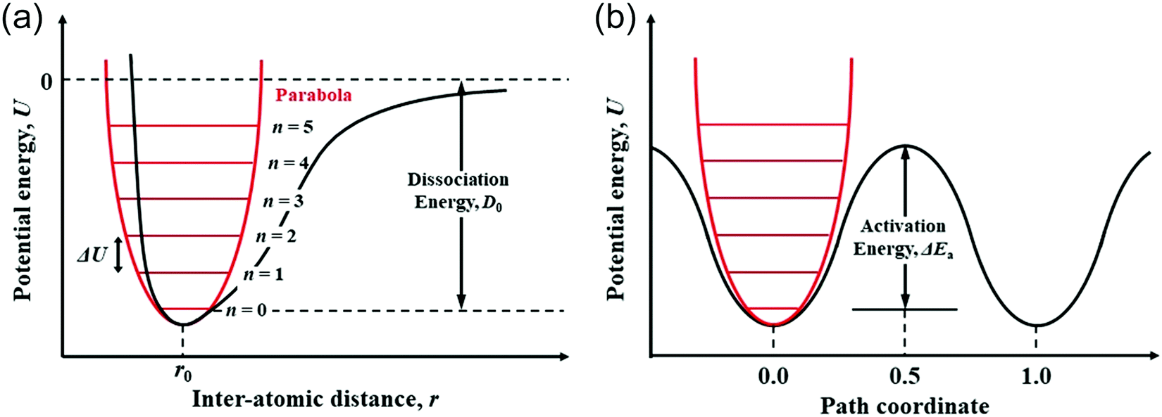 | ||
| Fig. 10 (a) Schematic relationship of the potential energy of two atoms with interatomic distance and (b) schematic potential energy of the migrating atom along the migration pathway. | ||
We found that the Einstein temperature of the Cu–Se bond is lower than that of In–Se and Ga–Se bonds in CIGSe using an XAFS analysis.69 We believe that the force constant, k, of the Cu–Se bond is smaller than those of In–Se and Ga–Se bonds, because the reduced mass of the Cu–Se bond with μ = 5.85 × 10⁻²⁶ kg is smaller than those of the In–Se bond with μ = 7.77 × 10⁻²⁶ kg and Ga–Se bond with μ = 6.15 × 10⁻²⁶ kg. The potential energy curve of the Cu–Se bond with small force constant rises slowly with increasing interatomic distance from r0. The result shows that the Cu–Se bond more easily stretches than other bonds. We previously evaluated the formation energies of Cu, In/Ga and Se vacancies in CISe and CGSe and showed that the formation energy of a Cu vacancy was smaller than those of the other vacancies.70 The result indicates that the dissociation energy, D0, in Fig. 10a is smaller for the Cu–Se bond than those for other bonds. The potential energy curve of the Cu–Se bond is a broad parabola with a shallower ground state than those of the In–Se and Ga–Se bonds. Therefore, the activation energy of Cu migration, ΔEa, which is the difference between the ground state and the energy at transition state shown in Fig. 10b, is smaller than those of In and Ga migrations. The Cu atom in the stretchy Cu–Se bond easily hops over the low activation energy and moves to a nearby Cu vacancy site. The XAFS result is consistent with the present result shown in Fig. 8a.
4.3 Theoretical calculation of atomic migration in Ag(In,Ga)Se2
The activation energies of the migration of Ag, In, and Ga atoms in AIGSe with [Ag]/([Ga] + [In]) ratio of 15/16 are shown in Fig. 8b. As in the case of CIGSe, the activation energy of the group I element (Ag) migration is the smallest and that of In is smaller than that of Ga at any GGI ratio. Compared to the CIGSe system, the activation energy of Ag migration in AgInSe2 (AISe) is smaller than that of Cu migration in CISe. The result suggests that Ag atom in AIGSe more easily diffuse than Cu in CIGSe. The activation energies of In and Ga migration are also smaller in the AISe than in the CISe system. Shafarmann's group at the University of Delaware observed the microstructure of (Cu,Ag)(Ga,In)Se2 films with large grains. The alloying of Ag in CIGSe film contributes to the growth of CIGSe crystalline grains.71Fig. 9b shows variations in the interatomic distances between the migrating Ag atom and the neighboring Se atoms in AISe along the migration pathway. In the initial and final states, group I atom (Ag) is tetrahedrally surrounded by Se(1), Se(2), Se(3), and Se(4) and by Se(4), Se(6), Se(7), and Se(8), respectively. The Ag–Se bond lengths (2.641 Å) in the initial and final states are in good agreement with the sum of covalent radii of Ag (1.473 Å) and Se (1.145 Å).67 As in the case of CISe system, group I atom (Ag) migrates from the initial state surrounded by four Se atoms to the transition state through the state surrounded by three Se atoms. In the transition state, the migrating Ag atom passes through the coordinate positions (0.464, 0.677, 0.666) that is offset in the x-axis and z-axis direction from the octahedral site of the Se atoms (0.382, 0.626, 0.626). At the transition state, the Ag atom is surrounded by five Se atoms, Se(2), Se(3), Se(4), Se(6), and Se(7). The Ag–Se(4) bond of 2.53 Å is shorter than the initial Ag–Se bond of 2.63 Å and the Ag–Se(3) and Ag–Se(6) bond lengths are 2.80 Å while the Ag–Se(2) and Ag–Se(7) bond lengths are 2.98 Å. These bond lengths are longer than the sum of their covalent radii and shorter than the sum of van der Waals radii of Ag (1.70 Å) and Se (1.90 Å). Ag atom approaches Se(5) atom, but their interaction is very small, because the inter-atomic distance of Ag–Se(5) is considerably longer than the sum of their van der Waals radii.
The activation energy of the migrating atom depends on the interatomic distances between the migrating atom and the neighboring atoms in the transition state. In order to compare the migration of Cu in CISe and that of Ag in AISe, the interatomic distances between each migrating atom (Cu or Ag) and the neighboring Se atoms was normalized by the initial distances, 2.45 Å for Cu–Se in CISe and 2.641 Å for Ag–Se in AISe. Fig. 9c shows the normalized variations of the interatomic distances between the migrating Cu and the neighboring Se atoms along the migration pathway. In the transition state, the normalized interatomic distance of Cu–Se(4) is 0.98 and those of the other Cu–Se bonds, Cu–Se(2), Cu–Se(3), Cu–Se(6), and Cu–Se(7), are about 1.14. Fig. 9d shows the normalized variations of the interatomic distances between the migrating Ag and the neighboring Se atoms. In the transition state, the normalized inter-atomic distance of Ag–Se(4) is 0.96, those of Ag–Se(3) and Ag–Se(6) are about 1.06, and those of Ag–Se(2) and Ag–Se(7) are about 1.12. Thus, in the transition state, the normalized interatomic distance are smaller for Ag migration in AISe than for Cu migration in CISe. In particular, the normalized Ag–Se(3) and Ag–Se(6) lengths are clearly smaller than the corresponding Cu–Se(3) and Cu(6) lengths. We think that the small normalized interatomic distance in this transition state is one of reasons why the activation energy of Ag movement in AISe is smaller than the activation energy of Cu movement in CISe. From the viewpoint of the crystal structure of the chalcopyrite compounds, we estimate that the Ag–Se bond is weaker than the Cu–Se bond.72
5 Growth of CuGaSe2
CIGSe is a good material for both single-junction and tandem-type solar cells: we can control the bandgap energy from 1.0 eV to 1.7 eV by varying the GGI ratio, and a 1.4 eV material which is suitable for single-junction solar cells is available with a GGI of about 60% and a 1.7 eV CuGaSe2 (CGSe) which is applicable for tandem-type solar cell as a top cell is also available derived from these quaternary materials.73,74 Although the highest efficiency6 was obtained using a relatively low Ga composition, the degradation of VOC for high-Ga content CIGSe solar cells is still an open issue, and this problem must be addressed to boost the CIGSe solar cell efficiency further. In this section, one of the limitation mechanisms leading to the difficulty of the growth of high-quality CIGS films with high GGI values is discussed, and a possible solution is suggested.5.1 Crystal structure of precursor layers for CuInSe2 and CuGaSe2
Films were grown by the conventional three-stage method using substrate temperatures of 350 °C during the first stage and 550 °C during the second and third stages. The crystal structure of the precursor layers was firstly examined by the XRD measurements, and it was found that the crystal structure of the Ga–Se precursor changed from layered GaSe to α-Ga2Se3, a defect zinc blende structure, with increasing [Se]/[Ga] beam flux ratio ranging from 15 to 45 for CGSe. However, only the γ-In2Se3 phase, a defect wurtzite structure, could be grown with a [Se]/[In] beam flux ratio ranging from 25 to 45 for CISe. CGSe or CISe layers were subsequently grown using these three precursors. In the experiment, the duration of the second stage was slightly shortened compared with the duration required for growth of stoichiometric CGSe or CISe to clarify the role of Cu diffusion into the precursor layer, thus CGI ratio was smaller than 1.Fig. 11 shows cross-sectional SEM images and EDX maps of the samples. The cross-sectional samples were polished using ion beam etching. The Cu and Ga (In) atomic distributions were measured by EDX. It is noteworthy that the Cu and Ga (In) distribution was uniform when the precursor layer had a defect-zinc blende structure or a defect-wurtzite structure. However, when growth was started from the layered GaSe precursor, the result was completely different: Cu atoms obviously accumulated in the surface region, and the Ga atoms remain at the bottom of the film which is the layered GaSe layer. Therefore, it is concluded that Cu atoms easily diffuse into the α-Ga2Se3 or γ-In2Se3 precursor and that the Ga (In) atoms also easily diffuse out from the precursor, forming the chalcopyrite structure. On the contrary, Cu and Ga diffusion is difficult between the layered and chalcopyrite structures. STEM images were also taken for further confirmation of this phenomena, and the same results were observed (not shown). The results show that the crystal structure of the precursor should be the defect-zinc blende structure or the defect-wurtzite structure to enhance atomic diffusion for the growth of chalcopyrite materials and that the Se beam flux intensity during the first stage is important to maintain the precursor crystal structure for wider bandgap CIGSe with high-Ga content. The importance of the Se beam flux intensity for the high-Ga CIGSe has been also pointed out in the literature.75
 | ||
| Fig. 11 Cross-sectional SEM images and EDX maps of CGSe and CISe samples. The upper sample was grown from a layered GaSe precursor, the middle using a α-Ga2Se3 precursor, and the bottom for a γ-In2Se3 precursor. The red dots indicate high intensity signals and the blue dots low intensity signals in the EDX maps. The cross-section of the samples was polished by ion beam etching. | ||
5.2 Effects of Cu2−xSe flux on the growth of CuInSe2 and CuGaSe2
It is believed that Cu2−xSe acts as flux for the growth of CIGSe,76 however, its effect on CGSe is still open question, therefore the effect on CGSe growth was examined. In the experiments, extremely Cu-rich CISe or CGSe layers were grown by the three-stage method, so the duration of the second stage was intentionally elongated exceeding the time required to reach the stoichiometric point. The samples were removed after the second stage. Fig. 12 shows cross-sectional STEM images for extremely Cu-rich CISe and CGSe films, and TEM-EDX maps of elemental Cu distribution are also shown on the right-hand side. The CGI ratios were found to be about 3 for CISe and 8 for CGSe by surface SEM-EDX measurements, respectively. | ||
| Fig. 12 Cross-sectional STEM images of Cu-rich CISe (upper) and CGSe (lower) samples. The right-hand images show the TEM-EDX mapping of Cu atoms for each sample. | ||
The penetration of Cu2−xSe into the film is clearly observed in the CISe film as shown in Fig. 12, and excess Cu2−xSe is found to accumulate around CISe grain boundaries (GBs). Thus, grain growth of CISe is clearly a consequence of the flux effect of Cu2−xSe, and the average grain size is about 1.5 μm which is comparable to the film thickness. On the contrary, Cu2−xSe segregates on top of the CGSe. Grain growth is only observed in the upper part of the film, and the grain size is apparently small towards the bottom of the film. Voids are also observed in the lower part of the film in which insufficient grain growth occurs. The film compositions were measured point-by-point with a TEM-EDX analysis. The [Cu]/[Se] ratio was about 0.51 in the CISe grains, and it was about 2.1 in the Cu2−xSe region. Interestingly, the value was about 0.49 at the CISe GBs, therefore, the [Cu]/[Se] ratio was almost stoichiometric in the final CISe layer, even though it was grown under extremely Cu-rich conditions. The ratio was also examined for the CGSe film, and it was about 0.54 for the upper part of the film (the larger grain area) and 0.50 for the lower part of the film (the smaller grain area). The value was 2.0 in the Cu2−xSe area. It can be concluded from this analysis that CGSe has a tendency to become off stoichiometric and that Cu2−xSe acts as flux for the CISe growth, however, the effect is small or limited in case of the CGSe growth. Furthermore, the grains of the CISe film are smooth and voids were not observed in the image. On the other hand, voids and defects were observed in the CGSe grains. Since the CISe grains are surrounded by liquid Cu2−xSe during growth, the stress accumulated in the grains could be released by the liquid-phase Cu2−xSe, which leads to the growth of high quality CISe films. This mechanism is not be expected apply to CGSe growth, resulting in the formation of defects. The possible reason for this difference is the lattice constant dissimilarity. The in-plane lattice constant of CISe is 0.578 nm,77 and is 0.579 nm for Cu2−xSe,78 so they are lattice matched, but the corresponding value for CGSe is 0.560 nm,79 thus the difference is large between Cu2−xSe and CGSe. Furthermore, the stacking sequence of the Se sub-lattice changes during the CISe growth from ABAB…, to ABABCABABC…, and finally ABCABC…, however this sequence change does not occur during CGSe growth: the sequence remains ABCABC. Therefore, it could be speculated that the number of defects is reduced during this lattice re-arrangement process in the CISe growth, but not for CGSe growth, resulting more defects being present in the CGSe film. A real-time X-ray analysis of the CISe and CGSe growth has been also studied by H. R. Alvarez.80
5.3 Growth of CuGaSe2 from Cu2−xSe flux and its solar cell performance
In the previous section, the difficulty of the CGSe growth has been reviewed. In order to overcome this difficulty, a new growth process was investigated. The new growth sequence is shown in Fig. 13a. The process consists of two stages: the Cu2−xSe layer is grown first on a Mo coated glass substrate both to use the flux effects of Cu2−xSe and to enhance Ga diffusion. Then Ga and Se atoms are supplied to the precursor layer in the second stage. This growth process is the reverse process of the first and second processes in the three-stage method; the growth of the III-Se precursor, and then a Cu–Se supply. | ||
| Fig. 13 (a) Schematic sequence of a new CGSe growth process, and (b) a cross-sectional SEM image of the resulting CGSe film. | ||
A cross-sectional SEM image (non-polished) is shown in Fig. 13b. In this growth method, stoichiometry control was difficult. The lower part of the sample shows a stoichiometric CGSe with a larger grain size which indicates the flux effect of Cu2−xSe, but the upper part is a Cu-poor CGSe layer due to a longer Ga irradiation time. Emissivity monitoring81,82 may be effective to determine the end point of the growth.
Fig. 14 shows the J–V characteristic of a CGSe solar cell fabricated on a Mo coated glass substrate. The cell structure was glass/Mo/CGSe/CdS/ZnO:B. The CdS and ZnO layers were grown by chemical bath deposition and a metal–organic chemical vapor deposition process, respectively. The cell characteristics were evaluated under the AM 1.5, 100 mW cm−2 irradiance: the efficiency was 6.81%, the VOC for 0.609 V, JSC for 19.2 mA cm−2, and FF for 0.583. Although this was a preliminary result, it successfully demonstrated the growth of device-grade CGSe was possible by the proposed technique.
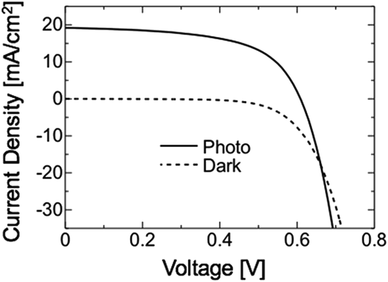 | ||
| Fig. 14 J–V characteristic of the CGSe solar cell grown by the proposed process. | ||
6 Over 22%-efficient Cd-free and all-dry process Cu(In,Ga)(S,Se)2 solar cells prepared with aged absorber layers
Fabrication of CIGSe and CIGSSe solar cells has been reported with different buffer layers.6,7,19,20,83–89 A 23.35%-efficient Cd-free CIGSSe solar cell with a Cs-treated CIGSSe absorber was obtained using a Zn(O,S,OH)x buffer, which was deposited using a wet chemical bath deposition (CBD) process.6 It has been recently reported that the 22%-efficient Cd-free and all-dry process CIGSSe solar cells are fabricated utilizing a Zn1−xMgxO buffer, which is inducive to the fabrication of not only an eco-friendly solar cell but also offers the possibility of further reductions in production costs.83,88 Therefore, the Cd-free and all-dry process CIGSSe solar cell is worthy of further development.In this research, CIGSSe films deposited by a selenization/sulfurization process have relatively high In and S content near the CIGSSe surface,88,89 possibly present in the form of InxSy near the surface. It is therefore suggested that the oxidized surface In- and S-rich CIGSSe thin films should give rise to the formation of Inx(O,S)y and/or a modified buffer near the CIGSSe surface to avoid sputtering damage to the CIGSSe absorber surface, thereby enhancing the photovoltaic efficiency (η).
Cd-free CIGSSe solar cells were thus fabricated using sputtered Zn1−xMgxO buffers by an all-dry process, where aged CIGSSe absorbers with and without alkali (Cs or K) treatment for different aging times up to 10 months (for the oxidized CIGSSe surface) are utilized. The effect of the aging time of the CIGSSe absorbers on photovoltaic performance as well as the carrier recombination rate was investigated for high performance Cd-free and all-dry process CIGSSe solar cells.
Cd-free and all-dry process CIGSSe solar cells with the structure of glass/Mo/CIGSSe/Zn0.8Mg0.2O buffer/Zn0.9Mg0.1O:B or Zn0.9Mg0.1O:Al were therefore fabricated with aged CIGSSe absorbers with and without K or Cs treatment. In the fabrication of the solar cell, CIGSSe absorbers were first prepared on Mo-coated glass substrates at Idemitsu Kosan Co., Ltd, which is discussed elsewhere.90–93 For the aged CIGSSe thin films (or the oxidized CIGSSe surface), the finished CIGSSe thin films were then kept in a desiccator cabinet containing a low O partial pressure of approximately 200 Pa under different aging times up to 10 months named the aging process. After the aging process, a Zn0.8Mg0.2O buffer layer and a Zn0.9Mg0.1O:Al transparent conductive oxide (TCO) layer were deposited by a co-sputtering process, as well as Zn0.9Mg0.1O:B as TCO layer was prepared by metal–organic chemical vapor deposition.83,88 Finally, Ni and Al grids were formed by electron beam evaporation. It is noted that the CdS-buffered CIGSSe solar cells using the aged CIGSSe absorbers were also fabricated for comparison, which is discussed elsewhere.83,88 The post-treatment HLS + LS process, including heat-light soaking (HLS) and followed by light-soaking (LS), were performed on all finished CIGSSe solar cells.94,95 The photovoltaic parameters (JSC, VOC, FF, η) were measured under equivalent AM 1.5G illumination. Moreover, the carrier recombination rates (Ri0, Rd0, and Rb0) throughout the Cd-free and all-dry process CIGSSe solar cells were quantitatively evaluated using temperature-illumination-dependent VOC measurements,96–99 where Ri0, Rd0, and Rb0 are the voltage-independent recombination rates at the buffer/absorber interface, space charge, and quasi-neutral regions, respectively.
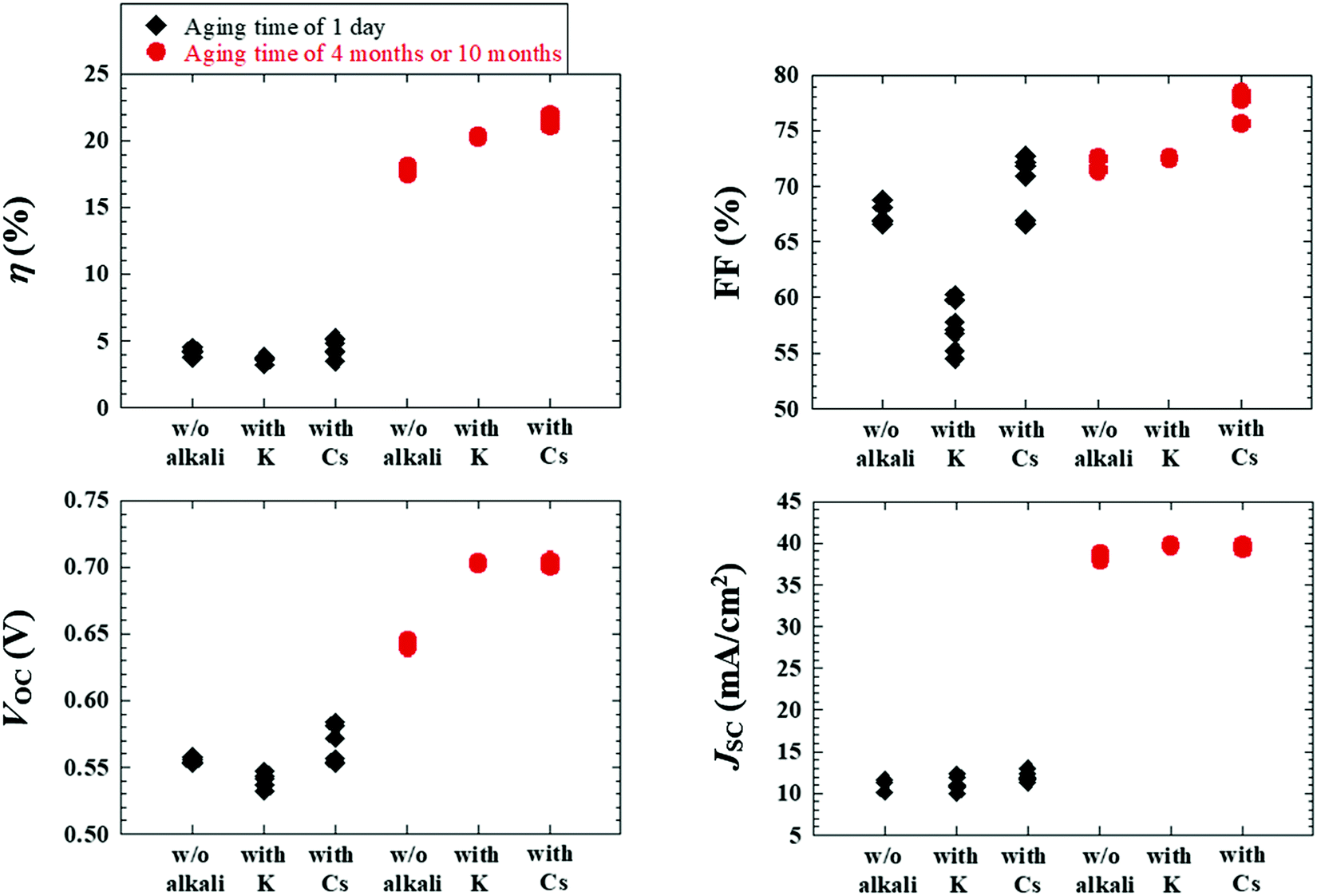
As a result, Fig. 15 depicts the photovoltaic parameters of Cd-free and all-dry process CIGSSe solar cells utilizing aged CIGSSe absorbers with aging times of 1 day, as well as 4 months or 10 months, where absorbers with and without alkali (Cs or K) treatment were used. Fig. 16 presents (a) the corresponding J–V characteristics and (b) external quantum efficiency (EQE) spectra of the Cd-free and all-dry process CIGSSe solar cells with the highest η values for each condition in Fig. 15, where the photovoltaic performance is shown in Table 1. The CdS-buffered CIGSSe solar cells using aged CIGSSe absorbers with and without alkali (Cs or K) treatment were moreover fabricated under different aging times. The photovoltaic parameters are shown in Fig. 17 and Table 1. According to these results, the photovoltaic performance of the Cd-free and all-dry process CIGSSe solar cells was significantly enhanced with η in the range of 18–22% for aging times of 4 months or 10 months regardless of alkali treatment, whereas those of the CdS-buffered CIGSSe solar cells remained almost constant. It is noted that the highest η of 22.6% for the Cd-free and all-dry process CIGSSe solar cell with Cs-treated CIGSSe absorber was obtained for an aging time of 10 months. The results suggest that the aging effect only plays an important role in increasing the η of the Cd-free and all-dry process CIGSSe solar cell irrespective of alkali treatment, whereas the aging effect has no impact on the η of the CdS-buffered CIGSSe solar cells.
 | ||
| Fig. 15 Photovoltaic performance of Cd-free and all-dry process CIGSSe solar cells using aged CIGSSe absorbers for aging times of 1 day, as well as 4 months or 10 months, where the absorbers with the alkali (Cs or K) treatment and without (w/o) alkali treatment are utilized. | ||
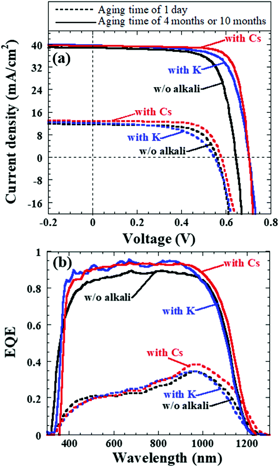 | ||
| Fig. 16 (a) Corresponding J–V characteristics and (b) EQE spectra of Cd-free and all-dry process CIGSSe solar cells using aged CIGSSe absorbers for aging times of 1 day, as well as 4 months or 10 months, where the absorbers with the alkali (Cs or K) treatment and without (w/o) alkali treatment are utilized. | ||
| Alkali treatment | Aging time of CIGSSe | J SC (mA cm−2) | V OC (V) | FF (%) | η (%) | |
|---|---|---|---|---|---|---|
| Cd-free and all-dry process CIGSSe solar cells | Without | 1 day | 11.6 | 0.557 | 68.8 | 4.4 |
| 4 months | 38.2 | 0.646 | 72.6 | 18.0 | ||
| K | 1 day | 12.0 | 0.546 | 57.7 | 3.7 | |
| 10 months | 39.7 | 0.702 | 72.5 | 20.2 | ||
| Cs | 1 day | 12.8 | 0.576 | 71.8 | 5.3 | |
| 10 months | 39.7 | 0.706 | 78.5 | 22.0 | ||
| CdS-buffered CIGSSe solar cells | Without | 1 day | 36.1 | 0.672 | 75.5 | 18.3 |
| 4 months | 36.4 | 0.671 | 74.1 | 18.1 | ||
| K | 1 day | 36.8 | 0.680 | 76.4 | 19.1 | |
| 10 months | 37.9 | 0.677 | 75.0 | 19.2 | ||
| Cs | 1 day | 38.6 | 0.705 | 79.0 | 21.5 | |
| 10 months | 38.9 | 0.710 | 78.3 | 21.7 | ||
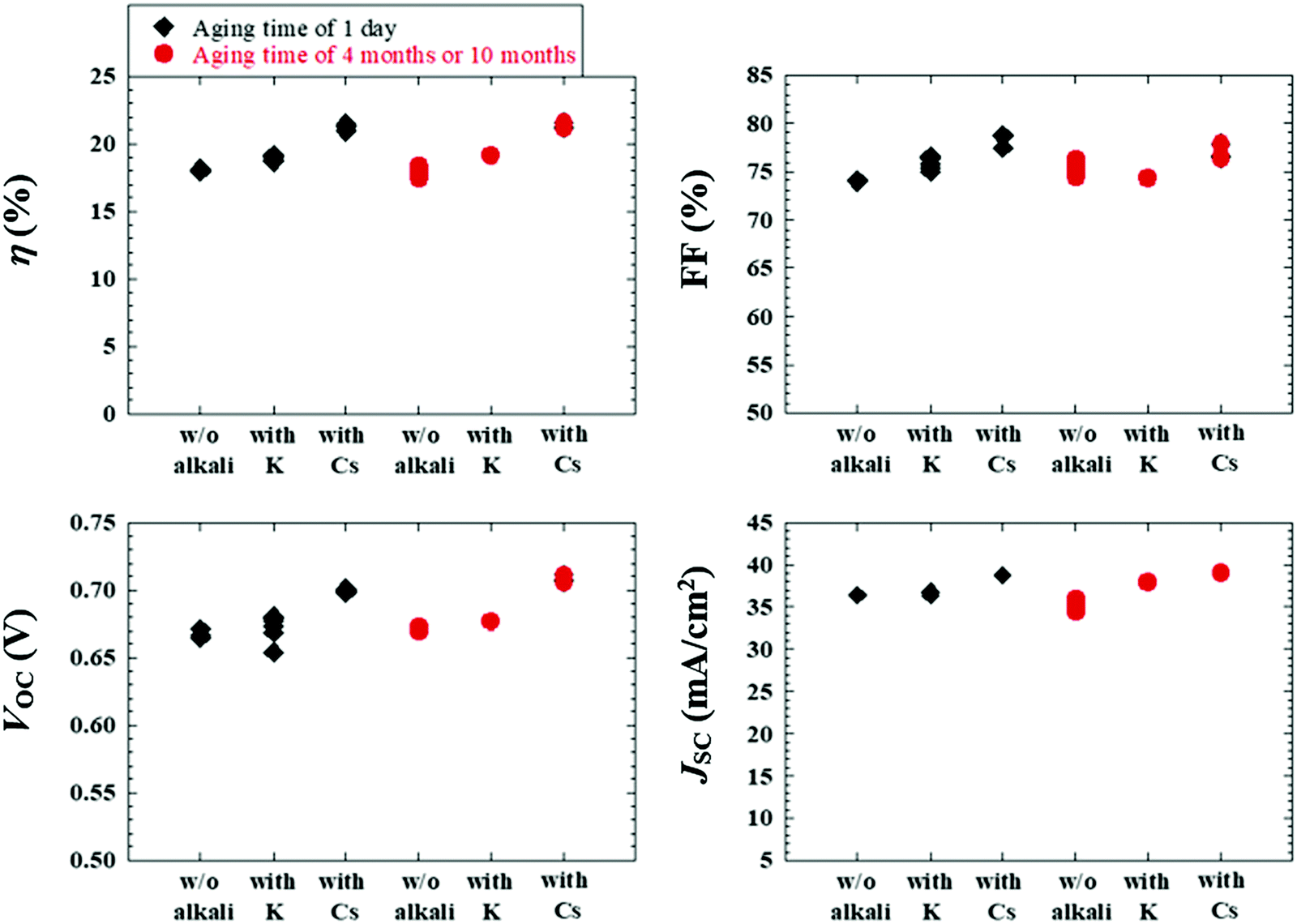 | ||
| Fig. 17 Photovoltaic performance of the CdS-buffered CIGSSe solar cells using aged CIGSSe absorbers for aging times of 1 day, as well as 4 months or 10 months, where the absorbers were processed with and without the alkali (Cs or K) treatment. | ||
Furthermore, the Ri0, Rd0, and Rb0 values throughout the Cd-free and all-dry process CIGSSe solar cells are estimated.96–99 It was found that for aging times from 1 week to 10 months the Ri0 and Rd0 decreased from about 3.3 × 10⁶ to 1.0 × 105 cm−2 s−1 and from approximately 7.7 × 10¹¹ to 7.4 × 1010 cm−2 s−1, respectively, whereas Rb0 remained constant at ∼2.0 × 105 cm−2 s−1. This implies that the CIGSSe bulk quality did not deteriorate, while the interface and near-surface qualities of the CIGSSe absorbers improved. The reduced Ri0 and Rd0 values confirmed that the oxidized CIGSSe surface should lead to the formation of a native Inx(O,S)y buffer layer (or modified layer) in the near-surface region of the CIGSSe absorber, thereby improving the charge separation and acting as a hole-blocking barrier while avoiding sputtering damage to the CIGSSe absorber surface. The improvement in charge separation is clearly reflected by the significant enhancement in EQE of the Cd-free and all-dry process CIGSSe solar cells for longer aging times, as shown in Fig. 16b. The aging effect resulting in the improvement of charge separation has been explained in detail in previous reports.88,89 As a result, the η of the Cd-free and all-dry process CIGSSe solar cell was found to greatly increase for longer aging times as can be seen in Table 1 as well as Fig. 15 and 16.
To examine the formation of native Inx(O,S)y buffer layers near the CIGSSe surface for increasing aging times, grazing-incidence X-ray diffraction (GIXRD) measurements as well as oxygen (O) content measurements in the near-surface region of bare CIGSSe thin films were investigated. Fig. 18 therefore illustrates the GIXRD patterns of the near-surface region of bare CIGSSe thin films (glass/Mo/CIGSSe) for different aging times of 1 day, and 10 months. It was confirmed that the InS and In2S3 peaks seen in the GIXRD patterns became more intense for aging times up to 10 months. Moreover, the O content near CIGSSe surface increased for longer aging times (not shown) as observed by SEM-EDX, suggesting the presence of an oxidized CIGSSe surface. We also found that the surface of aged CIGSSe samples showed evidences of Na segregation for long aging times, suggesting that Na catalytic effects accelerate the oxidation of the surface.89 The results consequently imply the incorporation of O into InS and In2S3 to form thin native In(O,S) and In2(O,S)3 (or Inx(O,S)y) near the CIGSSe surface with increased aging times. This is attributed to the low standard molar enthalpy (ΔfH0) values of InS (−138.1 kJ mol−1), In2S3 (−427.0 kJ mol−1), and In2O3 (−925.8 kJ mol−1) at 298.15 K.88
 | ||
| Fig. 18 GIXRD patterns of the near-surface region of the bare CIGSSe thin films (glass/Mo/CIGSSe) for aging times of 1 day, and 10 months. The incident angle of the GIXRD measurement was 0.1°, which corresponds to a corresponding penetration depth of approximately 55 nm into the CIGSSe. Powder diffraction files are denoted as PDF. | ||
In summary, aged CIGSSe absorber layers considerably boost photovoltaic performance of Cd-free and all-dry process CIGSSe solar cells regardless of alkali treatment. This takes place because aged CIGSSe thin films for longer aging times result in the formation of a native Inx(O,S)y buffer near the CIGSSe surface. This Inx(O,S)y or modified buffer/CIGSSe heterojunction acts as a heterojunction leading to charge separation and serves as a hole blocking barrier and also reduces sputtering damage. As a result, 22%-efficient Cd-free and all-dry process CIGSSe solar cells were obtained using aged Cs-treated CIGSSe absorbers.
7 Analysis of open circuit voltage loss
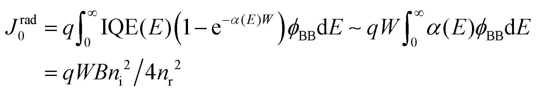
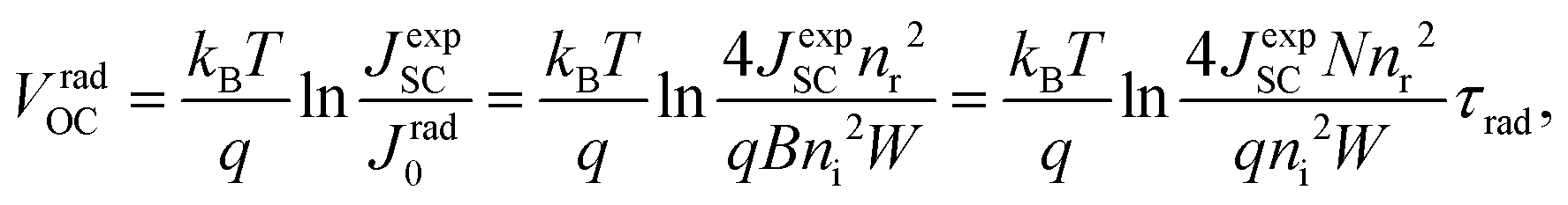
Suppressing recombination at the interface as well as in the bulk of solar cells leads to the improvement of cell performance. In order to achieve a photovoltaic efficiency of CISe-based solar cells close to the target of 25%, it is necessary to define where and to what extent recombination should be suppressed. The VOC deficit is a parameter commonly used that explains the energy loss of photovoltaic devices, however, which type of recombination affects this voltage loss should be clarified.100 Here, we show the results of sequential analysis of the recombination rate and energy loss of a CISe-based solar cell with world record level performance (η ∼ 23%).93First, the equation that is the premise of the VOC loss analysis is explained. The carrier recombination process corresponds to optical transitions in semiconductor materials, and its rate is governed by the recombination constant B. Specifically, the radiative recombination lifetime, τrad of minority carriers (in the case of CISe-based absorber layer, electrons) in the excited states (conduction band) can be expressed as
 | (1) |
 | (2) |
| Samples | GGI = 0 | GGI = 0.38 | GGI = 0.63 | GGI = 1 |
|---|---|---|---|---|
| Bandgap Eg (eV) | 1.04 | 1.275 | 1.436 | 1.68 |
| Intrinsic carrier density ni (cm−3) | 5.9 × 10⁹ | 6.3 × 10⁷ | 2.8 × 10⁶ | 2.5 × 10⁴ |
| Radiative recombination rate R0 (cm−3 s−1) | 3.5 × 10⁹ | 4.5 × 10⁵ | 6.6 × 10² | 6.7 × 10⁻² |
| Radiative recombination constant B (cm3 s−1) | 1.0 × 10⁻¹⁰ | 1.2 × 10⁻¹⁰ | 0.9 × 10⁻¹⁰ | 1.1 × 10⁻¹⁰ |
Next, the recombination analysis was conducted using the radiative recombination constant B. The maximum theoretical efficiency of a solar cell is typically expressed in terms of the Shockley–Queisser (SQ) limit, where all incident photons with energy above the band gap (Eg) of the absorber material are assumed to be converted to photocarriers without being linked to optical absorption loss.83 The saturation current density of the SQ limit (JSQ0) can be calculated by the generalized Planck's radiation law,107 which can be described by the following equation.
 | (3) |
 | (4) |
In thin-film solar cells, however, some photons do not contribute to the generation of photocarriers due to film thickness limitations and light absorption losses. Thus, the saturation current density in the radiative limit of thin-film solar cells can be obtained by the modified equation108,109
 | (5) |
 | (6) |
In an actual solar-cell device, there is a non-radiative recombination component. So, we have to take into account the presence of this recombination in the estimation of open-circuit voltage loss. We assumed the bulk recombination limit (VbulkOC), in which non-radiative recombination occurs significantly only in the quasi-neutral region (QNR). In actual devices, it is known that the depletion layer is prone to Shockley–Read–Hall (SRH) nonradiative recombination due to the presence of deep defect levels in the middle of the band gap.110 But in this estimation, in order to analyze each cause of energy loss separately and in an orderly manner, we ignore the non-radiative recombination in the depletion layer. In the bulk recombination limit, effective minority carrier lifetime, τeff, the saturation current density, Jbulk0, and the open-circuit voltage, VbulkOC, can be expressed by the following set of equations:
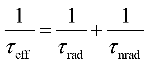 | (7) |
| Jbulk0 = qWni2/4p0nr2τeff | (8) |
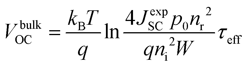 | (9) |
| Band gap Eg (eV) | Radiative recombination constant B (cm3 s−1) | Hole density p0 (cm−3) | Intrinsic carrier density ni (cm−3) | Refractive index nr | Absorber thickness (μm) | TRPL lifetime (ns) |
|---|---|---|---|---|---|---|
| 1.10 | 1.1 × 10⁻¹⁰ | 2 × 10¹⁶ | 2.36 × 10⁹ | 3 | 2 | 124 |
 | ||
| Fig. 19 Current–voltage characteristic curves derived under various calculation conditions or obtained experimentally. The obtained parameters, JSC and VOC, are listed in Table 4. | ||
| Calculation condition | J SC (mA cm−2) | V OC (V) |
|---|---|---|
| SQ limit | 44.2 | 0.858 |
| Radiative recombination limit | 38.5 | 0.824 |
| Bulk recombination limit | 38.5 | 0.791 |
| Experimental results | 38.5 | 0.746 |
Alkali metal treated CISe-based thin films are known to modify the surface and depletion layers in devices, but they are also known to contribute to the reduction of bulk defects.112 Antisite defects and defect complexes such as InCu, GaCu, and (InCu,GaCu) + 2VCu in the crystal grains and grain boundaries disappeared during the diffusion of alkali metal atoms, and as a result, the defect density involved in bulk recombination was reduced.113 For photoluminescence in CISe-based absorber layers, we have to consider bandgap grading; the luminescence was mainly induced at the position of the Eg minimum (400–500 nm deep from the surface, outside the depletion layer).114 In the CISe absorber layer with alkali metal treatment, which was utilized for the 22.9% efficiency device, the TRPL lifetime improved, suggesting that modification of the bulk quality.93 Furthermore, when deep defects at the entire absorber layers are reduced, recombination in the depletion layer was predicted to be suppressed.108 This may be the reason why bulk recombination has become dominant.
So, can raising of the efficiency from 23% to 25% be achieved simply by suppressing bulk recombination? If we take the recombination lifetime into account to calculate the radiation limit, it will be 824 mV. If the JSC and FF do not improve, it will be ∼25%. However, it is difficult in practice to reduce the non-radiative recombination component to zero.115 This suggests that 25% efficiency cannot be achieved by simply lowering bulk recombination. The decrease in photocurrent density due to the shadow of the grid electrode, absorption of the transparent conducting layer, recombination at the interface, and non-absorption of CIGSSe, in contrast, is estimated to be a few mA cm−2.83 Thus, reducing the absorption loss of the incident light, while suppressing the recombination component will be essential to achieve the 25% efficiency devices.
8 Depth directional profile of the electronic structure of the buffer/absorber region in high performance cells
Studies of CISe-based cells using absorbers fabricated by means of the three-stage co-evaporation over the last few decades have revealed the key factors for the realization of high performance such as the tuning of the band alignment at the buffer/absorber interface, the gradient in the band gap energy (Eg) along depth direction of the absorber and the control of alkali concentration after the formation of the absorber (alkali-PDT).19,20,116–119 Owing to intensive studies taking advantage of this knowledge, a high photovoltaic efficiency above 20% was reached by several institutes.19,20,116,120–123 Solar Frontier K. K. (Idemitsu Kosan Co., Ltd) has reported an efficiency above 22% for cells using CdS buffer layers.92 The current record photovoltaic efficiency of 23.35% using a Zn-based buffer was also reported by Solar Frontier.6 In both kinds of cells, CIGSSe quinary system compound formed by a selenization/surfurization process is used as the absorber. For deepening the understanding of device physics, it is useful to clarify how the above-mentioned knowledge is utilized in fabrication of high performance CIGSSe-based cells. This section summarize the directly determined depth-directional profiles of composition and electronic structure of the buffer/absorber region in CIGSSe-based cells by means of photoemission and inverse photoemission spectroscopy.The examined samples were CdS/CIGSSe bi-layers grown on Mo coated glass substrates. The CIGSSe layers were thinner than 2 μm. CIGSSe samples were provided by Solar Frontier. The samples were fabricated by selenization/sulfurization of metal precursors. Alkali-PDT was carried out for samples. Cells fabricated using identically fabricated CIGSSe absorbers and CdS buffers exhibited a photovoltaic efficiency above 20%. Prior to analysis, the samples were etched with a HN3 solution to remove contamination and heated in vacuum to desorb water. The surface composition and the VBM and CBM were determined by in situ measurements of X-ray, ultraviolet photoemission spectroscopy (XPS/UPS) and inverse photoemission spectroscopy (IPES), respectively. The Eg value obtained from IPES and UPS spectra had an error of ±0.15 eV. In order to access the interface between the absorber and the Mo contact for the above-mentioned characterization, we adopted a lift-off technique in a vacuum below 2 × 10⁻⁷ Pa, which allowed the cleaving of the CIGSSe/Mo/glass samples at the desired interface. Gluing the front surface of the CIGSSe/Mo/glass samples to a metal plate using a Ag-containing conductive epoxy allowed a subsequent separation at the CIGSSe/Mo interface. The vacuum environment of the lift-off and the in situ measurements yielded a surface free from contamination and alkali segregation. To determine the minimum band gap energy (Eg-min) of the CIGSSe layer, we utilized surface photovoltage (SPV) spectroscopy. For semiconductors under sufficiently low illumination intensity, the SPV can be assumed to be proportional to the absorption coefficient α of the semiconductor: SPV ∝ α.124 And for direct band gap semiconductors, α exhibits a square root dependence on the illumination energy for energies just above the band gap: α ∝ (hν − Eg)1/2, where ν is the frequency of the photon and h is the Planck constant.125 Therefore, for direct semiconductors, Eg can be extracted from a linear fit to the SPV increase when the spectrum is plotted as SPV2. For determining band alignment at the buffer/CIGSSe interface, a CdS buffer layer was deposited by stepwise evaporation of CdS onto the treated CIGSSe surface. To determine the band alignment at the CdS/CIGSSe interface, we adopted a two-step method. For the first step, the energetic differences in the VBM and the CBM between the surface of CIGSSe and of the thick CdS buffer layer were evaluated by means of UPS and IPES. Subsequently, the interface induced band bending (iibb) was determined from changes in the core level binding energies of the constituents of these layers in conjunction with CdS thickness. The band offsets were calculated by the combining the difference and the iibb. By using this procedure, the effect of the interface dipoles was automatically included in the deduced band alignment.
8.1 Depth-directional profiles in composition and electronic structure of the Cu(In,Ga)(S,Se)2 absorber
Table 5 shows a summary of the compositional ratios of the front- and back-surfaces of the CIGSSe absorber. The front surface is remarkably Ga-poor and S-rich. The [Cu]/([Ga] + [In]) (CGI) and anion/cation ratios were close to unity. These compositional ratios are close to those of chalcopyrite CuIn(S,Se)2. The bottom spectrum with the explanatory text “CdS 0 nm” in Fig. 20a and b are UPS and IPES spectrum of front surface of the CIGSSe, respectively. The VBM and CBM for the CIGSSe layers were −0.65 and +0.80 eV relative to Fermi level, respectively. Eg of 1.45 eV for this surface is slightly narrower than that of CuInS2, which is consistent with its S-rich, Ga-poor composition.72| GGI | CGI | [S]/([S] + [Se]) | ([S] + [Se])/([Cu] + [Ga] + [In]) | |
|---|---|---|---|---|
| CIGSSe front-surface | 0.05–0.06 | 0.92–0.94 | 0.81–0.89 | 0.90–0.92 |
| CIGSSe back-surface | 0.61 | 0.82 | 0.35 | 1.15 |
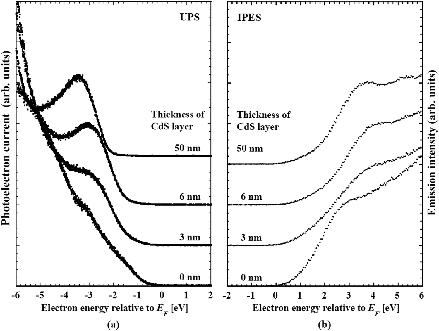 | ||
| Fig. 20 (a) Changes in the ultraviolet photoemission (UPS) spectra and (b) inverse photoemission (IPES) of CdS-buffer/CIGSSe-absorber structures in conjunction with the thickness of the CdS layer. In both figures, the bottom spectrum indexed with “0 nm” shows nature of the front-surface of the CIGSSe layer. | ||
We conclude that the front-surface of CIGSSe fabricated by a selenization/sulfurization process consists of a heavily S-substituted chalcopyrite phase. This is different from the composition of the so-called Cu-depleted defect phase: CGI below 0.625 and an anion/cation ratio above 1.25 which is intentionally formed on the front surface of the CIGSe absorber by the three-state coevaporation process to reduce surface recombination by the selective lowering of the VBM at the surface.77,126 A theoretical study about thermal equilibrium phase diagram of the Cu2S–In2S3 and Cu2S–In2S3–Ga2S3 systems reveals that Cu deficient compounds such as CuIn3S5 and Cu(In,Ga)3S5 are not formed.72,127 This is consistent with the absence of Cu-depleted compounds on the S-rich CIGSSe absorber surface.
In contrast with the front surface, the back-surface has a Ga-rich, S-poor characteristics. The CGI ∼ 0.8 and anion/cation ratio ∼1.25 values are close to the values of CuIn3(S,Se)5, a Cu-depleted defect compound. The change in crystalline phase can be attributed to a reduction in the S/(S + Se) ratio. These results reveal that there are steep depth-directional gradients in GGI and S/(S + Se) in the CIGSSe layer, and that, in contrast with the stoichiometric chalcopyrite-like feature of the front-surface, the Cu-depleted phase should be dominant on the back-surface. UPS/IPES spectra of back-surface of the CIGSSe layer are shown in Fig. 21. In comparison with the front, the back-surface has the wider Eg of 1.55 eV, and the VBM and CBM core located at higher energies. In CIGSSe-related phases, it has been established that the main consequence of a decrease in the S-substitution ratio are an increase in the VBM and a shrinkage in Eg while an increase in the GGI results in a preferential increase in the CBM and an increase in Eg.72 A CBM above +1.0 eV and an increase in Eg are attributed to an inversion in the GGI and S/(S + Se) ratios. For the latter, the increase in the GGI overcompensates the narrowing induced by a decrease in the S-substitution ratio. In addition, a rather broad feature in the conduction band edge of the back-surface indicates a steep gradient in the GGI along the depth direction.
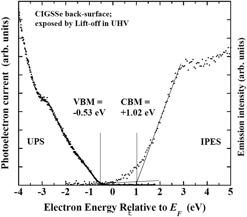 | ||
| Fig. 21 UPS and IPES spectra of the back-surface of the CIGSSe absorber layer exposed by lift-off in ultra-high vacuum. | ||
Fig. 22 shows the relationship between the square of excitation–photon intensity normalized surface photovoltage and the energy of the excitation-photon, of the CdS/CIGSSe structure. Since the diffusion length of photo-excited carriers in CISe-based cells is comparable to the depth of the region with Eg-min,128,129 the threshold energy of the excitation photon in the surface photovoltage spectrum (SPS) shows the Eg-min of the absorber.124,130 The observed Eg-min is 1.06–1.07 eV which is much smaller than the Eg of the front- and back-surface of the CIGSSe layer, which is evidence of the presence of a so-called double-graded depth-directional profile in Eg of the CIGSSe absorber. The value of Eg-min is close to the Eg of CuInSe2, which indicates that some parts of the interior region of the CIGSSe absorber is almost Ga free. Although the band edge positions of the interior region of the CIGSSe layers with a band gap energy of Eg-min are not determined yet, the Eg-min is similar to the Eg of CuInSe2. This suggests that the CBMs are also similar. We can estimate the CBM of the back-surface of the CIGSSe absorber should exceed that of the interior region by more than a few tenths of an eV. These results strongly suggest the presence of an adequate gradient in the CBM from the interior region to the back surface to form a so-called “back surface field.”131 Moreover, the Urbach energy (EU), which is extracted by fitting the subband gap SPV using the relationship of 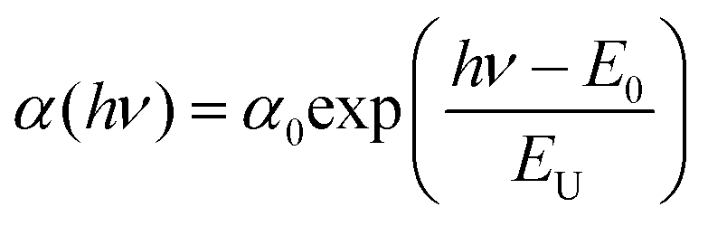 , where α0 and E0 are material dependent parameters,132 is in the range from 18–23 meV. It has been pointed out that an EU comparable or below thermal energy at room temperature is essential to realize a small open-circuit-voltage deficit and high photovoltaic efficiency.133 These results are, therefore, consistent with the observed high efficiency cells fabricated using identical CIGSSe absorber layers.
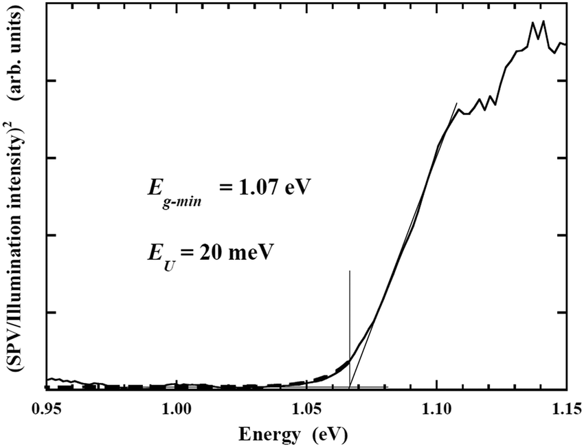 | ||
| Fig. 22 Relationship between the square of the illumination intensity normalized surface photovoltage (SPV) of the CdS/CIGSSe structure and the photon energy. Eg-min and EU are the minimum of the band gap energy and the Urbach energy of the CIGSSe absorber, respectively. SPV was measured in situ using a photo-assisted UHV Kelvin probe force microscope. The dashed fit line results from a fit of the subband gap SPV using the Urbach tails. | ||
8.2 Band alignment at the Cu(In,Ga)(S,Se)2/CdS interface
Band offsets at this heterointerface were calculated using the energy separation between the corresponding band-edge of the front surface of the CIGSSe and a 50 nm thick CdS layer, and the interface induced band bending, iibb. Changes in the UPS and IPES spectra of the CdS/CIGSSe structure in conjunction with the thickness of the CdS layer are shown in Fig. 20. The CBM and VBM of the surface of the 50 nm thick CdS are lower than the corresponding edge-position of the CIGSSe-front surface by 0.4 and 1.48 eV, respectively. Fig. 23 and Table 6 show changes in the XPS core signals of cations in the structure and the binding energies in conjunction with the CdS thickness. In the early stage of CdS deposition, the CIGSSe-related signals slightly decreased. On the other hand, as the CdS thickness increased, the Cd-signal exhibited a large increase. The averaged shifts in the binding energies of the CIGSSe- and CdS-related cations were −0.11 and +0.55 eV, respectively. The direction of the band bending was downward, and the total iibb was +0.44 eV. This large iibb is favorable for promoting carrier separation. By using these values, the band alignment at the CdS/CIGSSe interface was determined as shown in Fig. 24. The conduction band offset (CBO) was +0.04 eV and the valence band offset (VBO) was +1.04 eV. The former reveals that conduction band connection of this interface is an “small spike” and has an adequate height.118 The later implies the presence of a sufficient electronic barrier against hole-conduction. These values act to suppress recombination loss at the interface and act to promote electron transport. Therefore, we conclude that the CdS-buffer/CIGSSe-absorber interface has an ideal band alignment; large iibb and adequate band offset.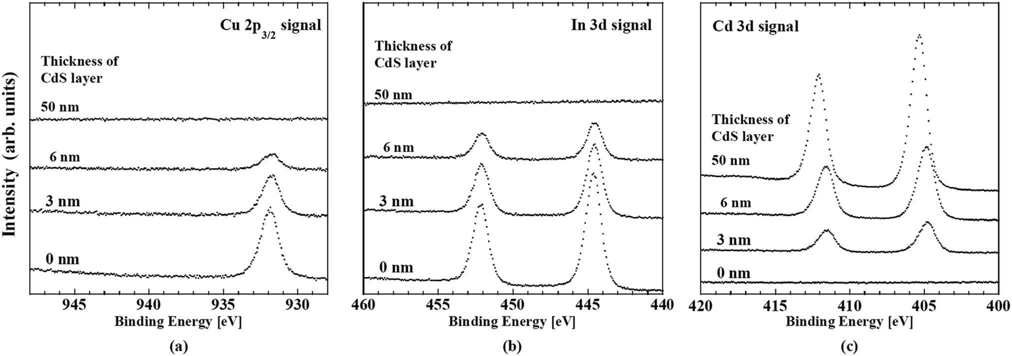 | ||
| Fig. 23 Changes in the (a) Cu 2p3/2, (b) In 3d and (c) Cd 3d XPS spectra of CdS/CIGSSe structures in conjunction with the thickness of the CdS layer. | ||
| CdS thickness (nm) | Core level binding energy (eV) | ||
|---|---|---|---|
| Cu 2p3/2 | In 3d5/2 | Cd 3d5/2 | |
| 0 (Front surface of the CIGSSe) | 931.97 | 444.65 | — |
| 3 | 931.84 | 444.60 | 404.85 |
| 6 | 931.81 | 444.58 | 404.92 |
| 50 | — | — | 405.40 |
 | ||
| Fig. 24 Schematic diagram of the band alignment of the CdS/CIGSSe interface. | ||
The depth-directional profiles of the electronic structure of the high performance CIGSSe cells characterized by the in situ spectroscopic measurements are as follows.
(i) Double graded profile of Eg in the CIGSSe absorber; the Eg of the front- and back-surface of the CIGSSe layer increase due to the presence of a high S/(S + Se) ratio and high GGI, respectively. The interior region, in contrast, has a narrow Eg close to that of CuInSe2.
(ii) The large CBM (not lower than +1.0 eV) of the back-surface and the narrow Eg of the interior region indicates the presence of a so-called back surface field.
(iii) The interface between the CdS buffer and the CIGSSe absorber has band offsets and band bending favorable for reducing the interface-recombination and promoting carrier transport. Visualization of the location and the width of Eg-min in interior region in the CIGSSe absorber is the next subject of research, since these are crucial parameters for the absorption of long wavelength light.
9 Summary
We reviewed the important physical and chemical issues facing CISe-based thin-film materials and devices based upon our recent studies.In Section 2, the role of Cu-deficient phases, which are often referred to as ordered vacancy compounds, and a correlation with alkali-metal beneficial effects were reviewed. Also, greater than 18% photovoltaic efficiency was demonstrated from a 17-cell monolithically integrated lightweight and flexible CIGSe solar minimodule. In Section 3, epitaxial and polycrystalline CIGSe film growth and device performance were comparatively studied. An epitaxial CIGSe solar cell yielded 21% photovoltaic efficiency, which was a value comparable to highly efficient polycrystalline devices. In Section 4, crystal growth of Ag(In,Ga)Se2 was discussed in comparison to Cu(In,Ga)Se2 growth. It was suggested that Ag–Se bonds are weaker than the Cu–Se bonds. This may affect elemental migration during growth leading to large grain growth in polycrystalline films upon Ag addition. In Section 5, a comparative study of three-stage process CISe and CGSe film growth was reviewed. It was found that undesirable defects likely form and remain in CGSe films. Thus, an alternative two-stage growth process was proposed to mitigate defect formation and to enhance CGSe-based solar cell performance. In Section 6, Cd-free and all-dry processed CIGSSe solar cells, which demonstrated over 22% photovoltaic efficiencies were reported. In Section 7, it was concluded that open circuit voltage loss likely occurs due to carrier recombination in CISe-based solar cells. Reducing the absorption loss of the incident light while suppressing the recombination component are essential to achieve 25% or higher photovoltaic efficiencies. In Section 8, an analysis of the electronic structure at the CdS/CIGSSe interface using direct and inverse photoelectron spectroscopy was summarized.
Author contributions
S. I. was responsible for writing Sections 1, 2, and 9, and also for finalizing the manuscript. J. N. wrote Section 3. K. B., T. M., F. A., and T. W. were responsible for writing Section 4 and A. Y. wrote Section 5. J. C., T. N., and T. M. were responsible for writing Section 6. M. M. I. and T. S. wrote Section 7 and N. T. wrote Section 8.Conflicts of interest
There are no conflicts to declare.Acknowledgements
S. Ishizuka and J. Nishinaga would like to thank H. Higuchi, H. Takahashi and M. Iioka for their help with the experiments and technical support. The authors also thank N. Taguchi, S. Tanaka, Y. Kamikawa, T. Masuda and P. J. Fons for fruitful discussions and continuous encouragement. J. Chantana, T. Nishimura, T. Minemoto and N. Terada thank researchers and engineers in Solar Frontier K. K. (Idemitsu Kosan Co., Ltd) particularly T. Kato, H. Sugimoto and Y. Kimoto for useful discussion and help with the experiments including sample supply. This work was supported by the New Energy and Industrial Technology Development Organization (NEDO) under the Ministry of Economy, Trade, and Industry (METI). This work was also supported in part by the JSPS KAKENHI under grant numbers 19K05282 and 20K05354, and a Mitsubishi Foundation Research Grant in the Natural Sciences No. 201910001.References
- S. Wagner, J. L. Shay, P. Migliorato and H. M. Kasper, Appl. Phys. Lett., 1974, 25, 434 CrossRef CAS.
- J. L. Shay, S. Wagner and H. M. Kasper, Appl. Phys. Lett., 1975, 27, 89 CrossRef CAS.
- L. L. Kazmerski, F. R. White and G. K. Morgan, Appl. Phys. Lett., 1976, 29, 268 CrossRef CAS.
- B. Dimmler and H. W. Schock, Prog. Photovoltaics, 1996, 4, 425 CAS.
- K. Kushiya, M. Tachiyuki, T. Kase, I. Sugiyama, Y. Nagoya, D. Okumura, M. Sato, O. Yamase and H. Takeshita, Sol. Energy Mater. Sol. Cells, 1997, 49, 277 CrossRef CAS.
- M. Nakamura, K. Yamaguchi, Y. Kimoto, Y. Yasaki, T. Kato and H. Sugimoto, IEEE J. Photovolt., 2019, 9, 1863 Search PubMed.
- T. Kato, A. Handa, T. Yagioka, T. Matsuura, K. Yamamoto, S. Higashi, J.-L. Wu, K. F. Tai, H. Hiroi, T. Yoshiyama, T. Sakai and H. Sugimoto, IEEE J. Photovolt., 2017, 7, 1773 Search PubMed.
- M. A. Green, E. D. Dunlop, J. Hohl-Ebinger, M. Yoshita, N. Kopidakis and X. Hao, Prog. Photovoltaics, 2021, 29, 657 Search PubMed.
- M. J. (Mariska) de Wild-Scholten, Sol. Energy Mater. Sol. Cells, 2013, 119, 296 CrossRef.
- K. Beppu, Y. Hirai, T. Kato, S. Ishizuka, T. Ina and T. Wada, Appl. Phys. Lett., 2020, 117, 043901 CrossRef CAS.
- J. Hedström, H. Ohlsén, M. Bodegård, A. Kylner, L. Stolt, D. Hariskos, M. Ruckh and H.-W. Schock, Conference Record of the 23rd IEEE Photovoltaic Specialists Conference, Louisville, USA, 1993, pp. 364–371.
- M. A. Contreras, B. Egaas, P. Dippo, J. Webb, J. Granata, K. Ramanathan, S. Asher, A. Swartzlander and R. Noufi, Conference Record of the 26th IEEE Photovoltaic Specialists Conference, Anaheim, USA, 1997, pp. 359–362.
- R. Caballero, C. A. Kaufmann, T. Eisenbarth, A. Grimm, I. Lauermann, T. Unold, R. Klenk and H. W. Schock, Appl. Phys. Lett., 2010, 96, 092104 CrossRef.
- L. M. Mansfield, I. L. Repins, S. Glynn, M. D. Carducci, D. M. Honecker, J. W. Pankow, M. R. Young, C. DeHart, R. Sundaramoorthy, C. L. Beall and B. To, Conference Proceedings of the 37th IEEE Photovoltaic Specialists Conference, Seattle, USA, 2011, pp. 3636–3641.
- P. Blösch, S. Nishiwaki, A. Chirilă, L. Kranz, C. Fella, F. Pianezzi, C. Adelhelm, E. Franzke, S. Buecheler and A. N. Tiwari, Thin Solid Films, 2013, 535, 214 CrossRef.
- S. Ishizuka, A. Yamada, K. Matsubara, P. Fons, K. Sakurai and S. Niki, Appl. Phys. Lett., 2008, 93, 124105 CrossRef.
- S. Ishizuka, A. Yamada, M. M. Islam, H. Shibata, P. Fons, T. Sakurai, K. Akimoto and S. Niki, J. Appl. Phys., 2009, 106, 034908 CrossRef.
- D. Rudmann, A. F. da Cunha, M. Kaelin, F. Kurdesau, H. Zogg, A. N. Tiwari and G. Bilger, Appl. Phys. Lett., 2004, 84, 1129 CrossRef CAS.
- A. Chirilá, P. Reinhard, F. Pianezzi, P. Bloesch, A. R. Uhl, C. Fella, L. Kranz, D. Keller, C. Gretener, H. Hagendorfer, D. Jaeger, R. Erni, S. Nishiwaki, S. Buecheler and A. N. Tiwari, Nat. Mater., 2013, 12, 1107 CrossRef PubMed.
- P. Jackson, R. Wuerz, D. Hariskos, E. Lotter, W. Witte and M. Powalla, Phys. Status Solidi RRL, 2016, 10, 583 CrossRef CAS.
- F. Pinanezzi, P. Reinhard, A. Chirilá, B. Bissig, S. Nishiwaki, S. Buecheler and A. N. Tiwari, Phys. Chem. Chem. Phys., 2014, 16, 8843 RSC.
- P. Reinhard, B. Bissig, F. Pianezzi, H. Hagendorfer, G. Sozzi, R. Menozzi, C. Gretener, S. Nishiwaki, S. Buecheler and A. N. Tiwari, Nano Lett., 2015, 15, 3334 CrossRef CAS PubMed.
- P. Reinhard, B. Bissig, F. Pianezzi, E. Avancini, H. Hagendorfer, D. Keller, P. Fuchs, M. Döbeli, C. Vigo, P. Crivelli, S. Nishiwaki, S. Buecheler and A. N. Tiwari, Chem. Mater., 2015, 27, 5755 CrossRef CAS.
- M. Malitckaya, H.-P. Komsa, V. Havu and M. J. Puska, J. Phys. Chem. C, 2017, 121, 15516 CrossRef CAS.
- S. Ishizuka, N. Taguchi, J. Nishinaga, Y. Kamikawa, S. Tanaka and H. Shibata, J. Phys. Chem. C, 2018, 122, 3809 CrossRef CAS.
- N. Taguchi, S. Tanaka and S. Ishizuka, Appl. Phys. Lett., 2018, 113, 113903 CrossRef.
- T. Lepetit, S. Harel, L. Arzel, G. Ouvrard and N. Barreau, Prog. Photovoltaics, 2017, 25, 1068 CAS.
- T. Kodalle, T. Bertram, R. Schlatmann and C. A. Kaufmann, IEEE J. Photovolt., 2019, 9, 1839 Search PubMed.
- S. Ishizuka and P. J. Fons, ACS Appl. Mater. Interfaces, 2020, 12, 25058 CrossRef CAS PubMed.
- S. Zahedi-Azad, M. Maiberg, R. Clausing and R. Scheer, Thin Solid Films, 2019, 669, 629 CrossRef CAS.
- S. Ishizuka and P. J. Fons, Phys. Rev. Appl., 2021, 15, 054005 CrossRef CAS.
- A. M. Gabor, J. R. Tuttle, D. S. Albin, M. A. Contreras, R. Noufi and A. M. Hermann, Appl. Phys. Lett., 1994, 65, 198 CrossRef CAS.
- B. Namnuan, V. Amornkitbamrung and S. Chatraphorn, J. Alloys Compd., 2019, 800, 305 CrossRef CAS.
- S. Ji, T. Hayakawa, N. Suyama, K. Nakamura and A. Yamada, Jpn. J. Appl. Phys., 2020, 59, 041003 CrossRef CAS.
- D. Schmid, M. Ruckh, F. Grunwald and H. W. Schock, J. Appl. Phys., 1993, 73, 2902 CrossRef CAS.
- S. Ishizuka, Appl. Phys. Lett., 2021, 118, 133901 CrossRef CAS.
- S.-H. Wei, S. B. Zhang and A. Zunger, J. Appl. Phys., 1999, 85, 7214 CrossRef CAS.
- E. Handick, P. Reinhard, J.-H. Alsmeier, L. Köhler, F. Pianezzi, S. Krause, M. Gorgoi, E. Ikenaga, N. Koch, R. G. Wilks, S. Buecheler, A. N. Tiwari and M. Bär, ACS Appl. Mater. Interfaces, 2015, 7, 27414 CrossRef CAS PubMed.
- D. Hauschild, D. Kreikemeyer-Lorenzo, P. Jackson, T. Magorian Friedlmeier, D. Hariskos, F. Reinert, M. Powalla, C. Heske and L. Weinhardt, ACS Energy Lett., 2017, 2, 2383 CrossRef CAS.
- T. Negami, N. Kohara, M. Nishitani, T. Wada and T. Hirao, Appl. Phys. Lett., 1995, 67, 825 CrossRef CAS.
- A. Hofmann and C. Pettenkofer, Appl. Phys. Lett., 2012, 101, 062108 CrossRef.
- K. Ueda, T. Maeda and T. Wada, Thin Solid Films, 2017, 633, 23 CrossRef CAS.
- C.-S. Jiang, R. Noufi, J. A. AbuShama, K. Ramanathan, H. R. Moutinho, J. Pankow and M. M. Al-Jassim, Appl. Phys. Lett., 2004, 84, 3477 CrossRef CAS.
- C. Leendertz, F. Streicher, M. Ch Lux-Steiner and S. Sadewasser, Appl. Phys. Lett., 2006, 89, 113120 CrossRef.
- M. Kawamura, T. Yamada, N. Suyama, A. Yamada and M. Konagai, Jpn. J. Appl. Phys., 2010, 49, 062301 CrossRef.
- M. Takihara, T. Minemoto, Y. Wakisaka and T. Takahashi, Prog. Photovoltaics, 2013, 21, 595 CAS.
- D. Keller, S. Buecheler, P. Reinhard, F. Pianezzi, B. Bissig, R. Carron, F. Hage, Q. Ramasse, R. Erni and A. N. Tiwari, Appl. Phys. Lett., 2016, 109, 153103 CrossRef.
- D. Abou-Ras, B. Schaffer, M. Schaffer, S. S. Schmidt, R. Caballero and T. Unold, Phys. Rev. Lett., 2012, 108, 075502 CrossRef PubMed.
- S. A. Jensen, S. Glynn, A. Kanevce, P. Dippo, J. V. Li, D. H. Levi and D. Kuciauskas, Appl. Phys. Lett., 2016, 120, 063106 Search PubMed.
- N. Taguchi, S. Tanaka and S. Ishizuka, private communication (unpublished).
- R. Carron, S. Nishiwaki, T. Feurer, R. Hertwig, E. Avancini, J. Löckinger, S.-C. Yang, S. Buecheler and A. N. Tiwari, Adv. Energy Mater., 2019, 9, 1900408 CrossRef.
- S. Ishizuka, A. Yamada, P. Fons and S. Niki, J. Renewable Sustainable Energy, 2009, 1, 013102 CrossRef.
- M. Raghuwanshi, E. Cadel, S. Duguay, L. Arzel, N. Barreau and P. Pareige, Prog. Photovoltaics, 2017, 25, 367 CAS.
- A. Vilalta-Clemente, M. Raghuwanshi, S. Duguay, C. Castro, E. Cadel, P. Pareige, P. Jackson, R. Wuerz, D. Hariskos and W. Witte, Appl. Phys. Lett., 2018, 112, 103105 CrossRef.
- S. Ishizuka, Y. Kamikawa, J. Nishinaga and T. Masuda, Presented at the 2021 International Conference on Solid State Devices and Materials, September 8, 2021. See http://www.ssdm.jp/index.html. Also, see S. Ishizuka, T. Yoshiyama, K. Mizukoshi, A. Yamada and S. Niki, Sol. Energy Mater. Sol. Cells, 2010, 94, 2052 CrossRef CAS for details of the minimodule structure and fabrication process.
- A. N. Tiwari, S. Blunier, M. Filzmoser, H. Zogg, D. Schmid and H. W. Schock, Appl. Phys. Lett., 1994, 65, 3347 CrossRef CAS.
- S. Niki, Y. Makita, A. Yamada, O. Hellman, P. J. Fons, A. Obara, Y. Okada, R. Shioda, H. Oyanagi, T. Kurafuji, S. Chichibu and H. Nakanishi, J. Cryst. Growth, 1995, 150, 1201 CrossRef CAS.
- D. J. Schroeder, J. L. Hernandez, G. D. Berry and A. A. Rockett, J. Appl. Phys., 1998, 83, 1519 CrossRef CAS.
- M. Fujita, A. Kawaharazuka, J. Nishinaga, K. H. Ploog and Y. Horikoshi, Jpn. J. Appl. Phys., 2011, 50, 125502 Search PubMed.
- D. Colombara, F. Werner, T. Schwarz, I. C. Infante, Y. Fleming, N. Valle, C. Spindler, E. Vacchieri, G. Rey, M. Guennou, M. Bouttemy, A. G. Manjón, I. P. Alonso, M. Melchiorre, B. E. Adib, B. Gault, D. Raabe, P. J. Dale and S. Siebentritt, Nat. Commun., 2018, 9, 826 CrossRef PubMed.
- J. Nishinaga, T. Nagai, T. Sugaya, H. Shibata and S. Niki, Appl. Phys. Express, 2018, 11, 082302 CrossRef.
- J. Nishinaga and T. Sugaya, Proceedings of the 47th IEEE Photovoltaic Specialists Conference, 2020, pp. 2251–2257.
- M. Fujita, T. Sato, T. Kitada, A. Kawaharazuka and Y. Horikoshi, J. Vac. Sci. Technol., B, 2012, 30, 02B126 CrossRef.
- S. Nakamura, T. Maeda and T. Wada, Jpn. J. Appl. Phys., 2013, 52, 04CR01 CrossRef.
- S. Nakamura, T. Maeda and T. Wada, Phys. Status Solidi A, 2013, 210, 1317 CrossRef CAS.
- S. Nishiwaki, T. Satoh, S. Hayashi, Y. Hashimoto, T. Negami and T. Wada, J. Mater. Res., 1999, 14, 4514 CrossRef CAS.
- P. Pyykkö, Phys. Rev. B: Condens. Matter Mater. Phys., 2012, 85, 024115 CrossRef.
- V. Gutmann, The donor-acceptor approach to molecular interaction, Plenum Press, New York, 1978 Search PubMed.
- K. Beppu, S. Yamazoe and T. Wada, submitted.
- T. Maeda and T. Wada, J. Phys. Chem. Solids, 2005, 66, 1924 CrossRef CAS.
- N. Valdes, J. Lee and W. Shafarman, Sol. Energy Mater. Sol. Cells, 2019, 195, 155 CrossRef CAS.
- T. Wada, Jpn. J. Appl. Phys., 2021, 60, 080101 CrossRef CAS.
- K. J. Tiwari, S. Giraldo, M. Placidi, A. G. Medaille, A. Thomere, S. Resalati, E. Saucedo and Z. J. Li-Kao, Sol. RRL, 2021, 5, 2100202 CrossRef CAS.
- T. Maeda, R. Nakanishi, M. Yanagita and T. Wada, Jpn. J. Appl. Phys., 2020, 59, SGGF12 CrossRef CAS.
- S. Ishizuka, A. Yamada, P. J. Fons, H. Shibata and S. Niki, Prog. Photovoltaics, 2014, 22, 821 CAS.
- S. Nishiwaki, N. Kohara, T. Negami, H. Miyake and T. Wada, Jpn. J. Appl. Phys., 1999, 38, 2888 CrossRef CAS.
- T. Maeda, W. Gong and T. Wada, Jpn. J. Appl. Phys., 2016, 55, 04ES15 CrossRef.
- K. Yamamoto and S. Kashida, J. Solid State Chem., 1991, 93, 202 CrossRef CAS.
- S. C. Abrahams and J. L. Bernstein, J. Chem. Phys., 1974, 61, 1140 CrossRef CAS.
- H. R. Alvarez, A. Weber, J. Lauche, C. A. Kaufmann, T. Rissom, D. Greiner, M. Klaus, T. Unold, C. Genzel, H.-W. Schock and R. Maiz, Adv. Energy Mater., 2013, 3, 1381 CrossRef.
- R. Scheer, A. Neisser, K. Sakurai, P. Fons and S. Niki, Appl. Phys. Lett., 2003, 82, 2091 CrossRef CAS.
- K. Sakurai, R. Hunger, R. Scheer, C. A. Kaufmann, A. Yamada, T. Baba, Y. Kimura, K. Matsubara, P. Fons, H. Nakanishi and S. Niki, Prog. Photovoltaics, 2004, 12, 219 CAS.
- J. Chantana, Y. Kawano, T. Nishimura, Y. Kimoto, T. Kato and H. Sugimoto, ACS Appl. Mater. Interfaces, 2020, 12, 22298 CrossRef CAS PubMed.
- S. Siebentritt, Sol. Energy, 2004, 77, 767 CrossRef CAS.
- D. Hariskos, S. Spiering and M. Powalla, Thin Solid Films, 2005, 480–481, 99 CrossRef CAS.
- D. Hariskos, B. Fuchs, R. Menner, N. Naghavi, C. Hubert, D. Lincot and M. Powalla, Prog. Photovoltaics, 2010, 17, 479 Search PubMed.
- T. Kobayashi, J. L. K. Zacharie, T. Kato, H. Sugimoto and T. Nakada, Prog. Photovoltaics, 2016, 24, 389 CAS.
- J. Chantana, T. Nishimura, Y. Kawano, N. Suyama, A. Yamada, Y. Kimoto, T. Kato, H. Sugimoto and T. Menemoto, Adv. Energy Mater., 2019, 9, 1902869 CrossRef CAS.
- T. Nishimura, J. Chantana, Y. Kawano, A. Yamada, Y. Kimoto, T. Kato, H. Sugimoto and T. Minemoto, Appl. Phys. Lett., 2020, 117, 223501 CrossRef CAS.
- T. Nakada, H. Ohbo, T. Watanabe, H. Nakazawa, M. Matsui and A. Kunioka, Sol. Energy Mater. Sol. Cells, 1997, 49, 285 CrossRef CAS.
- K. F. Tai, R. Kamada, T. Yagioka, T. Kato and H. Sugimoto, Jpn. J. Appl. Phys., 2017, 56, 08MC03 CrossRef.
- T. Kato, Jpn. J. Appl. Phys., 2017, 56, 04CA02 CrossRef.
- T. Kato, J. Wu, Y. Hirai, H. Sugimoto and V. Bermudez, IEEE J. Photovolt., 2019, 9, 325 Search PubMed.
- J. Chantana, T. Kato, H. Sugimoto and T. Minemoto, Prog. Photovoltaics, 2018, 26, 868 CAS.
- J. Chantana, Y. Kawano, T. Nishimura, T. Kato, H. Sugimoto and T. Minemoto, Sol. Energy, 2019, 184, 553 CrossRef CAS.
- S. Grover, J. V. Li, D. L. Young, P. Stradins and H. M. Branz, Appl. Phys. Lett., 2013, 103, 093502 CrossRef.
- J. V. Li, S. Grover, M. A. Contreras, K. Ramanathan, D. Kuciauskas and R. Noufi, Sol. Energy Mater. Sol. Cells, 2014, 124, 143 CrossRef CAS.
- J. Chantana, T. Kato, H. Sugimoto and T. Minemoto, Appl. Phys. Lett., 2018, 112, 151601 CrossRef.
- J. Chantana, T. Kato, H. Sugimoto and T. Minemoto, ACS Appl. Mater. Interfaces, 2018, 10, 11361 CrossRef CAS PubMed.
- J. F. Guillemoles, T. Kirchartz, D. Cahen and U. Rau, Nat. Photonics, 2019, 13, 501 CrossRef CAS.
- G. W. t’Hooft, Appl. Phys. Lett., 1981, 39, 389 CrossRef.
- H. T. Nguyen, S. C. Baker-Finch and D. Macdonald, Appl. Phys. Lett., 2014, 104, 112105 CrossRef.
- J. I. Pankov, Optical Processes in Semiconductors, Prentice-Hall, Englewood Cliffs, NJ, 1971, ch. 6 Search PubMed.
- S. Minoura, K. Kodera, T. Maekawa, K. Miyazaki, S. Niki and H. Fujiwara, J. Appl. Phys., 2013, 113, 063505 CrossRef.
- T. P. Weiss, R. Carron, M. H. Wolter, J. Löckinger, E. Avancini, S. Siebentritt, S. Buecheler and A. N. Tiwari, Sci. Technol. Adv. Mater., 2019, 20, 313 CrossRef CAS PubMed.
- M. H. Wolter, R. Carron, E. Avancini, B. Bissig, T. P. Weiss, S. Nishiwaki, T. Feurer, S. Buecheler, P. Jackson, W. Witte and S. Siebentritt, Prog. Photovoltaics, 2021, 1–11, DOI:10.1002/pip.3449.
- P. Würfel, S. Finkbeiner and E. Daub, Appl. Phys. A: Mater. Sci. Process., 1995, 60, 67 CrossRef.
- J. H. Werner, J. Mattheis and U. Rau, Thin Solid Films, 2005, 480-481, 399 CrossRef CAS.
- Y. He, I. Abdellaoui, M. Abdel-Shakour, T. Chowdhury, M. Kamarudin, A. Nogueira, Q. Shen, S. Hayase, A. Islam and T. Sakurai, Jpn. J. Appl. Phys., 2021, 60, SBBF13 CrossRef CAS.
- A. Lafuente-Sampietro, J. Chen, S. Wang, X. Hao, M. M. Islam, T. Kato, H. Sugimoto, K. Akimoto and T. Sakurai, Appl. Phys. Express, 2019, 12, 061001 CrossRef CAS.
- The recombination rate during open circuit voltage operation was estimated according to ref. 97 using the described rate parameters at thermal equilibrium from ref. 93.
- H. Tangara, S. Zahedi-Azad, J. Not, J. Schick, A. Lafuente-Sampietro, M. M. Islam, R. Scheer and T. Sakurai, J. Appl. Phys., 2021, 129, 183108 CrossRef CAS.
- T. Maeda, A. Kawabata and T. Wada, Jpn. J. Appl. Phys., 2015, 54, 08KC20 CrossRef.
- Y. Ando, S. Ishizuka, S. Wang, J. Chen, M. M. Islam, H. Shibata, K. Akimoto and T. Sakurai, Jpn. J. Appl. Phys., 2018, 57, 08RC08 CrossRef.
- M. Yamaguchi, L. Zhu, H. Akiyama, Y. Kanemitsu, H. Tampo, H. Shibata, K.-H. Lee, K. Araki and N. Kojima, Jpn. J. Appl. Phys., 2018, 57, 04FS03 CrossRef.
- R. Kamada, T. Yagioka, S. Adachi, A. Handa, K. F. Tai, T. Kato and H. Sugimoto, Proceedings of the 43rd IEEE Photovoltaic Specialists Conference, 2016, pp. 1287–1291.
- D. Colombara, K. Conley, M. Malitckaya, H.-P. Komsa and M. J. Puska, J. Mater. Chem. A, 2020, 8, 6471 RSC.
- T. Minemoto, T. Matsui, H. Takakura, Y. Hamakawa, T. Negami, Y. Hashimoto, T. Uenoyama and M. Kitagawa, Sol. Energy Mater. Sol. Cells, 2001, 67, 83 CrossRef CAS.
- M. Gloeckler and J. R. Sites, Thin Solid Films, 2005, 480–481, 241 CrossRef CAS.
- P. Jackson, D. Hariskos, E. Lotter, S. Paetel, R. Wuerz, R. Menner, W. Wischmann and M. Powalla, Prog. Photovoltaics, 2011, 19, 894 CAS.
- M. A. Green, K. Emery, Y. Hishikawa, W. Warta and E. D. Dunlop, Prog. Photovoltaics, 2013, 21, 1 Search PubMed.
- C. Jeong, T. Nagai, S. Ishizuka, H. Tampo, S. Hajime, S. Kim and Y. Kim, Phys. Status Solidi A, 2021, 218, 2000658 CrossRef CAS.
- M. Bär, I. Repins, M. A. Contreras, L. Weinhardt, R. Noufi and C. Heske, Appl. Phys. Lett., 2009, 95, 051206 CrossRef.
- L. Kronik and Y. Shapira, Surf. Sci. Rep., 1999, 37, 1 CrossRef CAS.
- T. S. Moss, Optical Properties of Semi-Conductors, Butterworths, London, 1956 Search PubMed.
- T. Wada, N. Kohara, S. Nishiwaki and T. Negami, Thin Solid Films, 2001, 387, 118 CrossRef CAS.
- A. Thomere, C. G. Deudona, M. T. Caldes, R. Bodeux, N. Barreau, S. Jobic and A. Lafond, Thin Solid Films, 2018, 665, 46 CrossRef CAS.
- K. Decock, J. Lauwaert and M. Burgelman, Energy Procedia, 2010, 2, 49 CrossRef CAS.
- G. Brown, V. Faifer, A. Pudov, S. Anikeev, E. Bykov, M. Contreras and J. Wu, Appl. Phys. Lett., 2010, 96, 022104 CrossRef.
- F. Streicher, S. Sadewasser and M. C. Lux-Steiner, Rev. Sci. Instrum., 2009, 80, 013907 CrossRef CAS PubMed.
- A. L. Sampietro, K. Yoshida, S. Wang, S. Ishizuka, H. Shibata, N. Sano, K. Akimoto and T. Sakurai, Sol. Energy Mater. Sol. Cells, 2021, 223, 110948 CrossRef.
- F. Urbach, Phys. Rev., 1953, 92, 1324 CrossRef CAS.
- J. Chantana, Y. Kawano, T. Nishimura, A. Mavlonov and T. Minemoto, Sol. Energy Mater. Sol. Cells, 2020, 210, 110502 CrossRef CAS.
| This journal is © the Owner Societies 2022 |