
Thermoelectric performance of ZrNX (X = Cl, Br and I) monolayers†
Wenwu
Shi
 ab,
Nina
Ge
c,
Xinzhong
Wang
*b and
Zhiguo
Wang
*ab
ab,
Nina
Ge
c,
Xinzhong
Wang
*b and
Zhiguo
Wang
*ab
aUniversity of Electronic Science and Technology of China, Chengdu, 610054, P. R. China. E-mail: zgwang@uestc.edu.cn
bDepartment of Electronic Communication and Technology, Shenzhen Institute of Information Technology, Shenzhen, 518172, China. E-mail: xzwang868@163.com
cState Key Laboratory of Environmental-friendly Energy Materials, Southwest University of Science and Technology, Mianyang, 621000, P. R. China
First published on 29th November 2021
Abstract
A low thermal conductivity and a high power factor are essential for efficient thermoelectric materials. The lattice thermal conductivity can be reduced by reducing the dimensions of the materials, thus improving the thermoelectric performance. In this work, the electronic, carrier and phonon transport and the thermoelectric properties of ZrNX (X = Cl, Br, and I) monolayers were investigated using density functional theory and Boltzmann transport theory. The electronic and phonon transport show anisotropic properties. The thermal conductivities are 20.8, 14.6 and 12.4 W m−1 K−1 at room temperature along the y-direction for the ZrNCl, ZrNBr, and ZrNI monolayers, respectively. Combining the low lattice thermal conductivity and the high power factor results in an excellent thermoelectric performance of the ZrNX monolayers. The thermoelectric figure of merit of ZrNX monolayers can reach magnitudes of ∼0.49–3.15 by optimal hole and electron concentrations between 300 and 700 K. ZrNX monolayers with high ZT values for n- and p-type materials would thus be novel, promising candidate 2D thermoelectric materials for heat–electricity conversion.
1. Introduction
Thermoelectric (TE) devices are solid-state devices that demonstrate environmentally friendly energy conversion between heat and electricity, and they show great potential for sustainable energy-conversion technology for harvesting waste heat and performing spot cooling with high reliability. The high TE performance of TE materials is necessary for the practical use of TE devices. The performance of TE materials is quantified by the dimensionless figure of merit (ZT). Theoretically, TE materials with a large ZT of above 3 become competitive with other energy-conversion systems, as the energy conversion efficiency between heat and electricity can reach 30%.1 According to the definition of ZT, i.e., ZT = S2σT/(κ),2 enhancement of the Seebeck coefficient (S) or the electronic conductivity (σ) and reduction of the thermal conductivity (κ) are efficient approaches for increasing the ZT value. The thermal conductivity (κ = κe + κl) is comprises the electronic (κe) and the lattice (κl) thermal conductivity. In most cases, the lattice thermal conductivity is the dominant mechanism in semiconductor materials. Anharmonic phonon–phonon scattering dominates the behaviour of the lattice thermal conductivity (κl) in crystalline semiconductors. Recently, Cammarata et al. identified phonon scattering selection rules3 and electrovibrational descriptors4 for possible phonon–phonon scattering channels, which is helpful for the discovery of 2D materials with desirable thermal properties, irrespective of their type of atomic topology and chemical composition. However, finding suitable TE materials with large ZT values is very challenging because of the strong correlation and coupling amongst these transport coefficients (S, σ, κe, and κl).5 For example, the electrical conductivity (σ) can be increased by increasing the carrier concentration, while the Seebeck coefficient (S) will be reduced and the electronic thermal conductivity (κe) will be increased with a higher carrier concentration.Layered materials, including typical covalent/ionic layered materials,6 artificial layered materials,7 and van der Waals layered materials,8,9 have long been investigated as promising TE materials. Various approaches have been proposed to optimize the ZT of TE materials, such as enhancing the electrical-transport properties via bandgap engineering10,11 and reducing the thermal conductivity using low-dimensional techniques.12,13 These approaches for the improvement of the ZT have been reviewed in ref. 14. Recently, it was reported that high-entropy materials show a high thermoelectric conversion efficiency.15 Thus, the thermoelectric performance of high-entropy thermoelectric materials can be improved through entropy engineering.16–18 Strong in-plane and weak out-of-plane bonding can modulate the electronic and phonon transport properties in van der Waals layered materials, thus achieving desirable TE performances. Reducing the dimensionality of TE materials has been proved to effectively improve the ZT value.19 Remarkable progress has been made in the study of two-dimensional (2D) materials as TE materials, and 2D materials show an enhanced TE performance over their corresponding bulk counterparts; for example, MX2 monolayers (M = Mo, W; and X = S, Se) show a better TE performance than their corresponding bulk counterparts.20
2D materials are potential candidates for fabricating thin solid and flexible thermoelectric devices, and various 2D materials have been widely studied. With recent advances in high-performance computing, researchers have paid great attention to discovering new 2D TE materials theoretically. The room-temperature ZT values for p-type carriers of 2H-MoS2, MoSe2, WS2, and WSe2 monolayers are between 0.7 and 0.9.21 High ZT values of 1.76 at 700 K, 2.32 at 700 K, and 3.95 at 500 K are predicted for p-type doping of GeSe, SnSe, and PbSe monolayers, respectively.22 The maximum ZT value of 3.46 can be achieved in the SnP3 monolayer via optimal p-type doping at 500 K.23 The GaTe monolayer shows a high p-type ZT of 0.91 and a weak dependence on the temperature and carrier concentration.24 The Ti2MoC2F2 monolayer has a ZT of 1.5 at 300 K and 3.1 at 800 K for a p-type carrier density of 1019 cm−3.25 The Mg3Sb2 monolayer can result in a low lattice thermal conductivity and a high power factor and consequently a high ZT (>2 at 600 K) has been reported for an n-type sample.26 For the SnSe monolayer with outstanding electronic transport properties, a high ZT value can reach up to 3.27 for n-type doping at 700 K.27 Compared with theoretical studies, experimental investigations on the TE performance of 2D materials are relatively scarce, especially the ZT values of 2D materials. Evaluation of the intrinsic ZT of 2D materials is technically difficult since the 2D material and its substrate form a parallel thermal circuit and the atomically thin thickness of 2D materials is much smaller than that of the substrate.28 The power factors for holes and electrons in a single crystalline graphene monolayer are estimated to be 6600 and 6100 μW m−1 K−2, respectively, at room temperature using the field-effect transistor structure.29 They are 4800 and 4100 μW m−1 K−2, respectively, at 250 K in a bilayer graphene flake on a Si/SiO2 substrate.30 The TE performance strongly depends on the substrate, and the power factors for holes and electrons are 36![[thin space (1/6-em)]](https://www.rsc.org/images/entities/char_2009.gif) 600 and 19000 μW m−1 K−2, respectively, for graphene on a hexagonal boron nitride substrate.31 The optimized n-type and p-type power factors are 3000 μW m−1 K−2 for ultrathin WSe2 single crystals,32 and the largest n-type power factor is 8500 μW m−1 K−2 in a bilayer MoS2 flake.33 A high ZT of ∼2.1 at 873 K has been reported in 2D Ge-doped SnSe nanoplates with thicknesses of 7–14 nm synthesized via a simple hydrothermal route.34 These results clearly imply the potential of 2D materials for achieving a higher thermoelectric performance for TE power generation and cooling applications. In general, a thermoelectric device is made from an n-type and a p-type TE material connected electrically; thus, n-type and p-type TE materials with a compatible performance are essential for devices. Although great improvements in TE performances have been achieved, it is difficult to achieve n-type and p-type TEs in one type of material.
600 and 19000 μW m−1 K−2, respectively, for graphene on a hexagonal boron nitride substrate.31 The optimized n-type and p-type power factors are 3000 μW m−1 K−2 for ultrathin WSe2 single crystals,32 and the largest n-type power factor is 8500 μW m−1 K−2 in a bilayer MoS2 flake.33 A high ZT of ∼2.1 at 873 K has been reported in 2D Ge-doped SnSe nanoplates with thicknesses of 7–14 nm synthesized via a simple hydrothermal route.34 These results clearly imply the potential of 2D materials for achieving a higher thermoelectric performance for TE power generation and cooling applications. In general, a thermoelectric device is made from an n-type and a p-type TE material connected electrically; thus, n-type and p-type TE materials with a compatible performance are essential for devices. Although great improvements in TE performances have been achieved, it is difficult to achieve n-type and p-type TEs in one type of material.
Transition metal nitride halides, MNX (M = Zr, Hf, Ti; and X = Cl, Br, I), are known for their superconductivity.35 MNX has two configurations, i.e., α-MNX with the FeOCl structure and β-MNX with the SmSI structure. Recently, MNX has attracted great attention due to its thermoelectric characteristics. Yu et al.36 investigated the thermal transport properties of β-ZrNCl and β-HfNCl bulk materials using DFT and found low in-plane thermal conductivity. MNX is a layered material with van der Waals binding between the layers. The MNX monolayer has also attracted much attention. As the β-form monolayer is more stable than the α-form monolayer, Yun et al.37 studied the thermoelectric properties of ZrNCl and HfNCl monolayers in the β-form, and the p-type ZrNCl monolayer was predicted to show a good thermoelectric performance. Liu et al.38 further studied the thermoelectric properties of β-ZrNCl and β-HfNCl monolayers at higher carrier concentrations and found that the HfNCl monolayer has a good thermoelectric transport performance and a high thermoelectric optimal value. The α-ZrNX (X = Cl, Br, or I) monolayer has also been proved to be stable, and the electronic properties of ZrNX (X = Cl, Br, or I) monolayers have been extensively studied using density functional theory (DFT) calculations,39,40 which indicates that ZrNX can be applied to 2D photohydrolytic catalysts. However, the thermoelectric performance of α-ZrNX has not yet been studied. In this work, the TE performance of ZrNX monolayers in the α-form was studied using DFT in combination with semiclassical Boltzmann transport theory (BTE). Great figures of merit were predicted for n- and p-type α-ZrNX (X = Cl, Br, or I) monolayers.
2. Simulation methods
DFT calculations were performed using the Vienna ab initio simulation package (VASP).41 For the description of the exchange–correlation functional, the generalized gradient approximation (GGA) parameterized by Perdew, Burke, and Ernzerhof (PBE) was used,42 and for the description of the electron–ion interaction, the projector augmented wave (PAW)43 method was used. The cut-off energy of the plane wave basis set was chosen to be 520 eV, which was tested for the convergence of the total energy. The first Brillouin zone integration was performed with a Γ-centred 7 × 6 × 1 Monkhorst–Pack grid for geometric optimization. All cell parameters and ion positions were relaxed until the maximum force on each atom was less than 0.01 eV Å−1, which was proved to be good enough to obtain convergence results. Using a maximum force on each atom of less than 0.001 eV Å−1 has a negligible effect on the lattice constant and band structures, as shown in Fig. S1 and Table S1 (ESI†). To avoid spurious interactions between periodic images in the direction perpendicular to the monolayer, a vacuum region of 30 Å was incorporated.The electronic transport properties were calculated by solving the electronic Boltzmann transport equation (BTE), as implemented in the BoltzTraP2 code.44 The calculations were performed under a constant relaxation time and rigid band approximations. A 48 × 42 × 1 k-mesh was used for evaluation of the Seebeck coefficient S and the electrical (σ/τ) and electronic thermal (κe/τ) conductivities, which are obtained as a function of the doping concentration along different directions at different temperatures using the following equations:
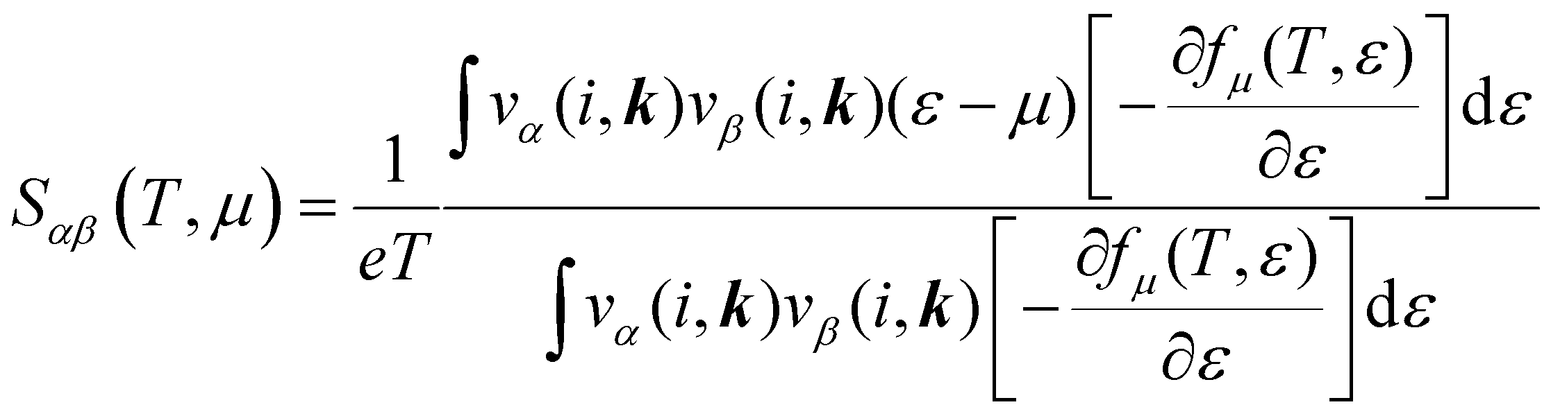 | (1) |
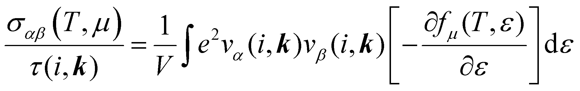 | (2) |
 | (3) |
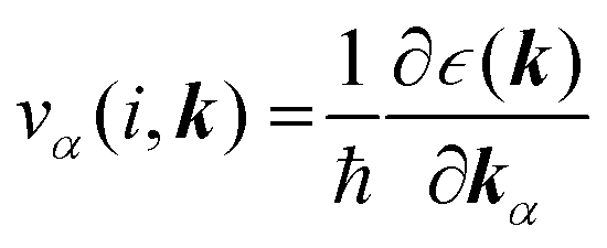 (α = x, y, z) is the group velocity;
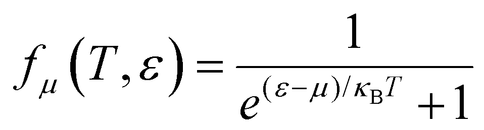 is the Fermi–Dirac distribution; and α and β denote the Cartesian components in the conventional unit cell.
Deformation potential (DP) theory45 was used to obtain the carrier relaxation time (τ). Based on DP theory, the τ value of a 2D material can be calculated using 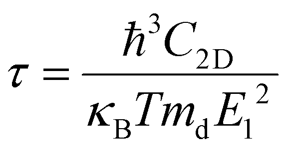 , where ħ, κB, and T are the Planck constant, Boltzmann constant, and absolute temperature, respectively;
 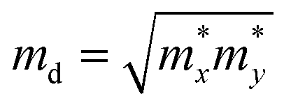 and is the average effective mass of the carrier effective mass along the x (
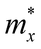 ) and y (
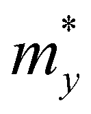 ) directions; E1 is the DP constant of the conduction-band maximum (CBM) for electrons or the valence-band minimum (VBM) for holes along the transport direction, which can be calculated via E1 = dEi/dδ, where Ei represents the energy change of the CBM or VBM under uniaxial strain δ.
 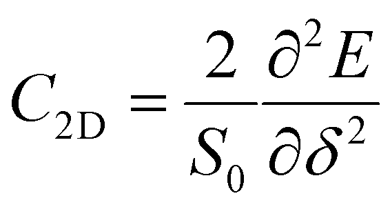 is the elastic modulus of the 2D material, where E is the total energy of the system, and S0 is the lattice area of the monolayer. In this work, δ values ranging from −2.0% to 2.0% are used to fit the values of C2D and E1.
Similarly, the lattice thermal conductivity (κl) was calculated by solving the phonon BTE using an iterative approach, as implemented in the ShengBTE code.46
 | (4) |
 is the phonon group velocity; α and β denote the Cartesian components in the conventional unit cell; and f0 is the Bose–Einstein distribution function. This code needs the second-order (harmonic) and third-order (anharmonic) interatomic force constants (IFCs) as inputs, which were all obtained using the real-space finite displacement difference method.47 The second-order IFCs and third-order IFCs were calculated on a 5 × 5 × 1 supercell with a Γ-centred 4 × 4 × 1 k-mesh using the Phonopy48 code and the thirdorder.py script as present in the ShengBTE code,46 respectively. The cut-off distances for the calculation of third-order IFCs were set to be 5.483, 5.527 and 5.612 Å for the ZrNCl, ZrNBr, and ZrNI monolayers, respectively. Using the convergence test, a dense 48 × 42 × 1 k-mesh was adopted when calculating the heat transport properties and the thermal conductivity.
From eqn (2)–(4), the electrical (σ/τ), electronic thermal (κe/τ), and lattice thermal (κl) conductivities depend on the volume of the unit cell. As a vacuum is considered to avoid spurious interactions between periodic images in the direction perpendicular to the monolayer, these obtained values from the code should be scaled. In this work, the calculated conductivities were normalized by multiplying c/d, where c is the cell length perpendicular to the monolayers, and d is the thickness of the layer. Here, the summation of the buckling distance and the van der Waals (vdW) radii of halogen atoms was taken as the thickness of the monolayer, which is 7.490, 7.938 and 8.515 Å for the ZrNCl, ZrNBr, and ZrNI monolayers, respectively.
3. Results and discussion
3.1 Structural and electronic properties
The ZrNX (X = Cl, Br, or I) monolayer shows an orthorhombic structure, which is similar to FeOCl. Each unit cell is composed of two Zr, two N and two halogen atoms. The side- and cross-sectional atomistic configurations of the ZrNX monolayer are shown in Fig. 1a. A buckling tetragonal Zr–N layer is sandwiched between halogen atomic layers in which the N atom is bonded to four neighbouring Zr atoms, each Zr atom is coordinated with four N atoms and two halogen atoms, and each halogen atom is bonded to two neighbouring Zr atoms. The optimized lattice constants are listed in Table 1 and agree well with the previously reported values.39,49 The lattice constant increases from 3.560 to 3.763 Å as the atomic radius of the X atom increases, while the lattice constant b shows a smaller change. The spin–orbit coupling (SOC) effect was not considered in this work as it has little effect on the band structures, as shown in Fig. S1 in the ESI.† The SOC effect negligibly affects the band structures of the ZrNCl and ZrNBr monolayers. The shape of the band structure is not affected by the SOC effect in the ZrNI monolayer, except for the 0.12 eV decrease in the bandgap. The small reduction in the bandgap is not expected to affect the main conclusion of this work. The band structures of the ZrNX monolayer are shown in Fig. 1b along a series of high symmetry points in the BZ. All ZrNX monolayers are semiconductors with direct bandgaps. The valence band maximum (VBM) and conduction band minimum (CBM) are located at Γ. The bandgaps of the ZrNCl, ZrNBr, and ZrNI monolayers are 1.75 eV, 1.72 eV and 1.28 eV, respectively. For the ZrNCl and ZrNBr monolayers, the hybridization of N 2p and Zr 4d orbitals dominantly contributes to the states near the Fermi level, and the Zr 4d and N 2p states contribute to the CBM and VBM, respectively. However, for the ZrNI monolayers, the CBM is mainly contributed by the Zr 4d orbital, and the VBM originates from the I 5p orbital. The effective masses of the electron and hole carriers ( and
and  , respectively) can be obtained by fitting the CBM and VBM. These calculated values are listed in Table 1. The value of
  along the x- and y-directions decreases with the increasing atomic mass of the halogen atom. However, the value of
  along the y-direction increases with the increasing atomic number of the halogen atom.
 | ||
| Fig. 1 (a) Top view and side view of the optimized ZrNX monolayers. (b) Band structure of the ZrNX monolayers. | ||
| a | b |
|
|
μ x | μ y | τ x | τ y | ||
|---|---|---|---|---|---|---|---|---|---|
| ZrNCl | e | 3.560 | 4.170 | 0.35 | 0.34 | 507 | 1343 | 98 | 258 |
| h | 0.31 | 0.71 | 216 | 2463 | 87 | 995 | |||
| ZrNBr | e | 3.635 | 4.164 | 0.30 | 0.32 | 571 | 1697 | 105 | 313 |
| h | 0.32 | 0.89 | 127 | 975 | 65 | 495 | |||
| ZrNI | e | 3.760 | 4.160 | 0.28 | 0.28 | 828 | 1765 | 133 | 284 |
| h | 0.19 | 1.10 | 72 | 880 | 45 | 550 |

3.2 Electronic transportation
The evolution of in-plane electronic transport coefficients (S, σ/τ, κe/τ, and S2σ/τ) with the hole and electron carrier concentrations can be obtained using the BoltzTraP2 code. The calculated electronic transport coefficients as a function of the carrier concentration are shown in Fig. 2. Here, the carrier concentration is changed from 5.0 × 10¹¹ to 5.0 × 1014 cm−2 at temperatures of 300, 500 and 700 K. As expected, the Seebeck coefficient decreases with the carrier concentration. For example, the Seebeck coefficient decreases from 460 to 44.2 μV K−1 as the hole concentration is increased from 5.0 × 10¹¹ to 5.0 × 1014 cm−2 at 700 K along the y-direction in the ZrNCl monolayer. Moreover, the Seebeck coefficient for the p-type carrier is slightly larger than that of the n-type carrier in the ZrNCl and ZrNBr monolayers, whereas the Seebeck coefficient for the p-type carrier is much larger than that of the n-type carrier in the ZrNI monolayer. The electrical conductivity (σ/τ) and electronic thermal conductivity (κe/τ) exhibit similar behaviour because they originate from the electronic band structure, which increases with the carrier concentration. σ and κe of the hole carrier show different behaviour in the transport direction in the ZrNX monolayer. They show less dependence on the transport direction in the ZrNCl monolayer, while they are much larger along the y-direction than along the x-direction in the ZrNBr and ZrNI monolayers. The large electrical transport coefficients along the zigzag direction may lead to high TE values along it. The difference arises because the CBM of the ZrNX monolayer is mainly contributed by the Zr 4d orbital, while the VBM is composed of states from different atoms in the ZrNCl, ZrNBr and ZrNI monolayers. Since the Seebeck coefficient shows opposite changes with electrical conductivity, the power factor with respect to the carrier concentration is shown in Fig. 2. The PF of p-type doping is visibly larger than that of n-type doping, especially in the ZrNI monolayer, which may be caused by the highest valence band being more flattened than the lowest conduction band. A high density of states is yielded at the flat portion, which induces a high S value and PF for p-type doping from the Mott relation.50 | ||
| Fig. 2 Calculated in-plane electronic transport coefficients (S, σ/τ, κe/τ, and S2σ/τ) as a function of the carrier concentration for p-type and n-type ZrNX monolayers at different temperatures. | ||
The carrier relaxation time (τ) calculated using deformation potential theory is presented in Table 1. The relaxation time depends on the carrier type and the crystalline direction. The relaxation times for electrons and holes are larger along the y-direction than along the x-direction. The relaxation time of electrons is larger than that of holes along the x-direction, but vice versa along the y-direction. For example, τx and τy are 98 and 258 fs, respectively, for electrons and 87 and 995 fs, respectively, for holes. The carrier mobility can also be estimated, using  . The carrier mobility along the x-direction is smaller than that along the y-direction, which reveals the mobility anisotropy. The electron mobilities are 507 and 1343 cm2 s−1 V−1 along the x- and y-directions, respectively. This result will lead to an anisotropic electronic contribution to the thermal conductivity.
3.3 Thermal transportation
Phonon dispersion is of great significance in the investigation of the lattice thermal conductivity. The calculated phonon dispersion along the high-symmetry k-point path in the first Brillouin zone and the phonon density of states (DOS) for the ZrNX monolayers are shown in Fig. 3. No imaginary frequency was found in the ZrNCl and ZrNBr monolayers, indicating the dynamic stability of the ZrNCl and ZrNBr monolayers. A negligible imaginary frequency (the largest imaginary frequency of approximately −7.94 cm−1) was observed in the ZrNI monolayer for the ZA and TA modes at the X-point (0.5, 0.0, 0.0). This sort of negative frequency is a common issue in first-principles calculations for 2D materials such as group-IV and III–V honeycomb monolayers51 and germanene.52 These imaginary branches originate from a computational artifact, which is not necessarily a sign of structural instability.53 These imaginary frequencies might be removed via more precise setups for the calculations, such as increasing the supercell size. Due to the substantial increase in the computational cost by increasing the supercell size for the VASP code, the PWmat code54 was used to calculate the phonon dispersion of the ZrNI monolayer. The imaginary frequency was observed for a 5 × 5 × 1 supercell; however, it disappears for a 6 × 5 × 1 supercell, as shown in Fig. S3 (ESI†). The dynamic stability of the ZrNI monolayer was also investigated using ab initio molecular dynamics by Zhang et al.,40 and the monolayer was not disrupted through 5 ps of MD simulation at 800 K, indicating that the ZrNI monolayer is dynamically stable. As can be seen from Fig. 3, the highest frequencies reach ∼746, ∼737, and ∼723 cm−1 for the ZrNCl, ZrNBr, and ZrNI monolayers, respectively. Detailed analysis of the phonon DOS shows that the phonon branches in the low-, medium-, and high-frequency regions are mainly contributed by halogen, Zr and N atoms, respectively. The phonon dispersion curves show that no phonon gap is present between the acoustic and optical branches, i.e., the lowest optical branches overlap with the acoustic branches, thus resulting in strong acoustic-optical interactions and the low lattice thermal conductivity of the ZrNX monolayers.55 The calculated lattice thermal conductivities of the ZrNX monolayers as a function of the temperature are shown in Fig. 4, and they decrease with increasing temperature. For example, κl decreases from 27 to 9 W m−1 K−1 along the x-direction as the temperature is increased from 300 to 900 K. The thermal conductivity is dominated by anharmonic phonon–phonon interactions56 since the thermal conductivity is inversely proportional to the temperature, as shown in Fig. 4. The thermal conductivity is larger along the x-direction than the y-direction, indicating a possible high thermoelectric performance along the y-direction. In addition, the thermal conductivity of the ZrNX monolayers decreases with the increasing atomic mass of the halogen atom at a given temperature. The small lattice thermal conductivity of the ZrNX monolayers could have a large value of ZT. The phonon velocity, Grüneisen parameter (γ) and phonon lifetime are calculated to further explore heat transport in the ZrNX monolayers, and are shown in Fig. 5. The group velocities near the Γ point are ∼6.7, ∼5.5 and ∼5.0 km s−1 for the ZrNCl and ZrNBr and ZrNI monolayers, respectively. The low phonon velocities can be attributed to the flat phonon dispersions, as shown in Fig. 3. These small phonon velocities and short relaxation times lead to low thermal conductivity in the ZrNX monolayers. The Grüneisen parameter γ can qualitatively describe the anharmonic interactions of crystal materials, and a large |γ| means that it might have strong phonon–phonon anharmonic scattering. From Fig. 5, |γ| increases with the increasing atomic mass of the halogen atom at low frequency, which agrees with the small thermal conductivity of the ZrNI monolayer. This phenomenon has been observed in KAgS and KAgSe monolayers.57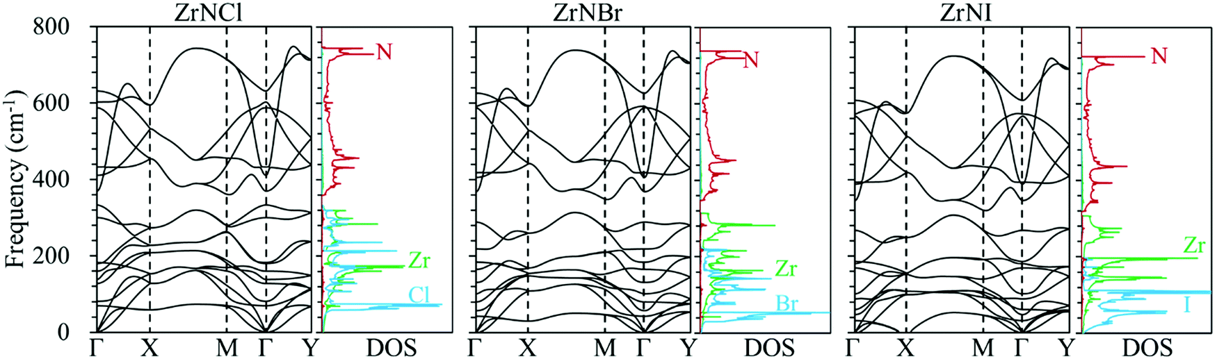 | ||
| Fig. 3 Phonon dispersion structure of the ZrNX monolayers along the highly symmetric k-point path in the first Brillouin zone and the corresponding atomic projected phonon density of states (DOS). | ||
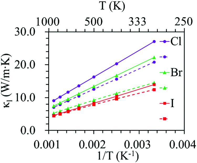 | ||
| Fig. 4 Lattice thermal conductivity of ZrNX monolayers as a function of temperature. The solid and dashed lines denote the thermal conductivity along the x- and y-directions, respectively. | ||
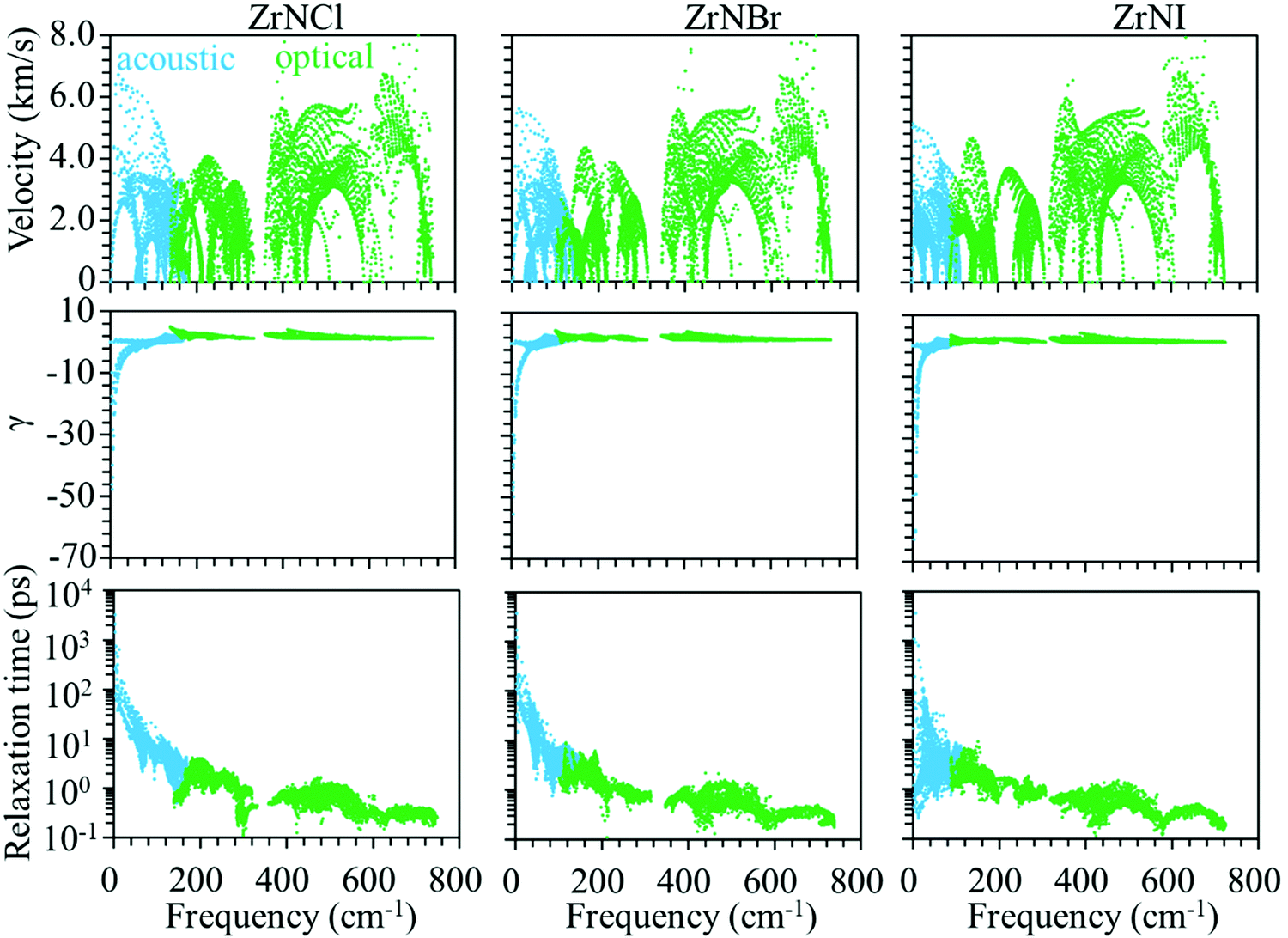 | ||
| Fig. 5 Group velocity, Grüneisen parameter (γ), and phonon lifetime of the ZrNX monolayers as a function of frequency. | ||
3.4 Figure of merit values
Based on the calculated lattice and electronic thermal conductivity and electronic transportation values, the ZT values with respect to the carrier concentration at 300, 500 and 700 K are shown in Fig. 6. The value of ZT increases with the carrier concentration to reach a maximum value and then decreases. The ZT is larger along the y-direction than along the x-direction for p-type and n-type doping. The ZT values increase with temperature, as the ZrNX monolayers have low thermal conductivities. The maximum ZT value for the hole carrier is larger than that for the electron carrier in the ZrNCl and ZrNI monolayers. The ZT values along the y-direction in the ZrNCl monolayer are 0.64, 1.64, and 2.48 for holes and 0.29, 0.78, and 1.27 for electrons at temperatures of 300, 500, and 700 K, respectively, with a carrier concentration of 2.0 × 1013 cm−2. The maximum ZT value for the hole carrier is close to that for the electron carrier in the ZrNBr monolayer. The maximum ZT values along the y-direction in the ZrNBr monolayer are 0.53, 1.24, and 1.91 for holes and 0.58, 1.16, and 1.77 for electrons at temperatures of 300, 500, and 700 K, respectively. Because of the low thermal conductivity in the ZrNI monolayer, it has a high thermoelectric performance. The maximum ZT values along the y-direction in the ZrNI monolayer are 0.73, 1.59, and 3.15 for holes and 0.49, 1.11, and 1.72 for electrons at temperatures of 300, 500, and 700 K, respectively. Our results indicate that n-type and p-type TE materials can be realized in ZrNX (X = Cl, Br, or I) monolayers for medium-temperature applications.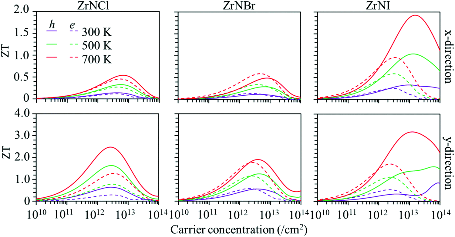 | ||
| Fig. 6 Figure of merit (ZT) of the ZrNX monolayers as a function of the carrier concentration at different temperatures along the x- and y-directions. | ||
4. Conclusion
In summary, the electronic, carrier and phonon transport and thermoelectric properties of ZrNX (X = Cl, Br, and I) monolayers were investigated using density functional theory and Boltzmann transport theory. All ZrNX monolayers are direct semiconductors with bandgaps of 1.75 eV, 1.72 eV and 1.28 eV for the ZrNCl, ZrNBr, and ZrNI monolayers, respectively. Electronic and phonon transport show anisotropic properties. The thermal conductivity along the x-direction is larger than that along the y-direction. The thermal conductivities are 20.8, 14.6 and 12.4 W m−1 K−1 at room temperature along the y-direction for the ZrNCl, ZrNBr, and ZrNI monolayers, respectively. Combining the low lattice thermal conductivity and the high power factor results in the excellent thermoelectric performance of the ZrNX monolayers. The thermoelectric figure of merit of the ZrNX monolayers can reach a magnitude of ∼0.49–3.15 at optimal hole and electron concentrations between 300 and 700 K. Since the 2D materials are atomically thin, rigid against mechanical strain and intrinsically flexible, they are suitable for practical flexible TE conversion devices. Abbas and Li58 proposed a thermoelectric generator structure based on monolayer MoS2. Oh et al.59 fabricated a TE generator with NbSe2 and WS2 nanosheets that uses the energy emitted by the human body, and this generator is flexible and durable and can be used as a glove-type wrist-band thermal sensor. The development of rigid and flexible thermoelectric generators for wearable and textile integration has been reviewed in ref. 60. The integration of 2D TE materials with other monolayers can generate multifunctionality, such as the integration of SnSe2 with graphene, producing superthermoelectric and mechanoelectric properties, which can be used as self-powered strain sensors that can continuously monitor the deformation of buildings and bridges to enhance safety.61 ZrNX monolayers with a high ZT for n- and p-type materials are thus promising novel candidates for 2D thermoelectric devices.Conflicts of interest
There are no conflicts of interest to declare.Acknowledgements
This work was financially supported by the open project of the State Key Laboratory of Environment-friendly Energy Materials (No. 19kfhg13).References
- J. Yang and T. Caillat, MRS Bull., 2011, 31, 224–229 CrossRef.
- F. J. DiSalvo, Science, 1999, 285, 703–706 CrossRef CAS PubMed.
- A. Cammarata, RSC Adv., 2019, 9, 37491–37496 RSC.
- A. Cammarata and T. Polcar, Phys. Rev. B, 2020, 102, 085409 CrossRef CAS.
- G. J. Snyder and E. S. Toberer, Nat. Mater., 2008, 7, 105–114 CrossRef CAS PubMed.
- L. D. Zhao, J. He, D. Berardan, Y. Lin, J. F. Li, C. W. Nan and N. Dragoe, Energy Environ. Sci., 2014, 7, 2900–2924 RSC.
- H. Ohta, S. Kim, Y. Mune, T. Mizoguchi, K. Nomura, S. Ohta, T. Nomura, Y. Nakanishi, Y. Ikuhara, M. Hirano, H. Hosono and K. Koumoto, Nat. Mater., 2007, 6, 129–134 CrossRef CAS PubMed.
- L. D. Zhao, S. H. Lo, Y. Zhang, H. Sun, G. Tan, C. Uher, C. Wolverton, V. P. Dravid and M. G. Kanatzidis, Nature, 2014, 508, 373–377 CrossRef CAS PubMed.
- W. D. Liu, L. Yang, Z. G. Chen and J. Zou, Adv. Mater., 2020, 32, 1905703 CrossRef CAS PubMed.
- J. P. Heremans, V. Jovovic, E. S. Toberer, A. Saramat, K. Kurosaki, A. Charoenphakdee, S. Yamanaka and G. J. Snyder, Science, 2008, 321, 554–557 CrossRef CAS PubMed.
- Y. Wu, B. Hou, C. Ma, J. Cao, Y. Chen, Z. Lu, H. Mei, H. Shao, Y. Xu, H. Zhu, Z. Fang, R. Zhang and H. Zhang, Mater. Horiz., 2021, 8, 1253–1263 RSC.
- X. Li, J. Liu, S. Li, J. Zhang, D. Li, R. Xu, Q. Zhang, X. Zhang, B. Xu, Y. Zhang, F. Xu and G. Tang, Nano Energy, 2020, 67, 104261 CrossRef CAS.
- E. Unsal, R. T. Senger and H. Sevinçli, Phys. Rev. B, 2021, 103, 014104 CrossRef CAS.
- Z. Ma, J. Wei, P. Song, M. Zhang, L. Yang, J. Ma, W. Liu, F. Yang and X. Wang, Mater. Sci. Semicond. Process., 2021, 121, 105303 CrossRef CAS.
- B. Jiang, Y. Yu, J. Cui, X. Liu, L. Xie, J. Liao, Q. Zhang, Y. Huang, S. Ning, B. Jia, B. Zhu, S. Bai, L. Chen, S. J. Pennycook and J. He, Science, 2021, 371, 830–834 CrossRef CAS PubMed.
- B. Jiang, Y. Yu, H. Chen, J. Cui, X. Liu, L. Xie and J. He, Nat. Commun., 2021, 12, 3234 CrossRef CAS PubMed.
- R. Liu, H. Chen, K. Zhao, Y. Qin, B. Jiang, T. Zhang, G. Sha, X. Shi, C. Uher, W. Zhang and L. Chen, Adv. Mater., 2017, 29, 1702712 CrossRef PubMed.
- Y. Luo, S. Hao, S. Cai, T. J. Slade, Z. Z. Luo, V. P. Dravid, C. Wolverton, Q. Yan and M. G. Kanatzidis, J. Am. Chem. Soc., 2020, 142, 15187–15198 CrossRef CAS PubMed.
- X. L. Shi, J. Zou and Z. G. Chen, Chem. Rev., 2020, 120, 7399–7515 CrossRef CAS PubMed.
- W. Huang, H. Da and G. Liang, J. Appl. Phys., 2013, 113, 104304 CrossRef.
- K. X. Chen, X. M. Wang, D. C. Mo and S. S. Lyu, J. Phys. Chem. C, 2015, 119, 26706–26711 CrossRef CAS.
- X. L. Zhu, C. H. Hou, P. Zhang, P. F. Liu, G. Xie and B. T. Wang, J. Phys. Chem. C, 2020, 124, 1812–1819 CrossRef CAS.
- X. L. Zhu, P. F. Liu, J. Zhang, P. Zhang, W. X. Zhou, G. Xie and B. T. Wang, Nanoscale, 2019, 11, 19923–19932 RSC.
- B. Marfoua and J. Hong, Nanotechnology, 2020, 32, 115702 CrossRef PubMed.
- S. Karmakar and T. Saha-Dasgupta, Phys. Rev. Mater., 2020, 4, 124007 CrossRef CAS.
- S. Huang, Z. Wang, R. Xiong, H. Yu and J. Shi, Nano Energy, 2019, 62, 212–219 CrossRef CAS.
- F. Q. Wang, S. Zhang, J. Yu and Q. Wang, Nanoscale, 2015, 7, 15962–15970 RSC.
- K. Kanahashi, J. Pu and T. Takenobu, Adv. Energy Mater., 2020, 10, 1902842 CrossRef CAS.
- D. Wang and J. Shi, Phys. Rev. B: Condens. Matter Mater. Phys., 2011, 83, 113403 CrossRef.
- S. G. Nam, D. K. Ki and H. J. Lee, Phys. Rev. B: Condens. Matter Mater. Phys., 2010, 82, 245416 CrossRef.
- J. Duan, X. Wang, X. Lai, G. Li, K. Watanabe, T. Taniguchi, M. Zebarjadi and E. Y. Andrei, Proc. Natl. Acad. Sci. U. S. A., 2016, 113, 14272–14276 CrossRef CAS PubMed.
- M. Yoshida, T. Iizuka, Y. Saito, M. Onga, R. Suzuki, Y. Zhang, Y. Iwasa and S. Shimizu, Nano Lett., 2016, 16, 2061–2065 CrossRef CAS PubMed.
- K. Hippalgaonkar, Y. Wang, Y. Ye, D. Y. Qiu, H. Zhu, Y. Wang, J. Moore, S. G. Louie and X. Zhang, Phys. Rev. B, 2017, 95, 115407 CrossRef.
- S. Chandra and K. Biswas, J. Am. Chem. Soc., 2019, 141, 6141–6145 CrossRef CAS PubMed.
- Y. Saito, T. Nojima and Y. Iwasa, Nat. Commun., 2018, 9, 778 CrossRef PubMed.
- X. Yu, H. Shao, X. Wang, Y. Zhu, D. Fang and J. Hong, J. Mater. Chem. A, 2020, 8, 3128–3134 RSC.
- W. S. Yun and J. D. Lee, Sci. Rep., 2017, 7, 17330 CrossRef PubMed.
- X. Liu, X. An, B. Xu, Q. Xia, G. Lu, G. Yu, J. Zhang, S. Ma, Y. Wang, J. Li, H. Dong and L. Yi, J. Solid State Chem., 2020, 290, 121500 CrossRef CAS.
- Q. D. Hao, Y. Luo, Z. Y. Zeng, X. R. Chen and Q. F. Chen, Solid State Commun., 2020, 322, 114049 CrossRef CAS.
- X. Zhang, Z. Zhang, X. Zhao, D. Wu, X. Zhang and Z. Zhou, J. Mater. Chem. A, 2017, 5, 2870–2875 RSC.
- J. Ran, J. Zhang, J. Yu, M. Jaroniec and S. Z. Qiao, Chem. Soc. Rev., 2014, 43, 7787–7812 RSC.
- J. P. Perdew, K. Burke and M. Ernzerhof, Phys. Rev. Lett., 1996, 77, 3865–3868 CrossRef CAS PubMed.
- G. Kresse and D. Joubert, Phys. Rev. B: Condens. Matter Mater. Phys., 1999, 59, 1758–1775 CrossRef CAS.
- G. K. H. Madsen, J. Carrete and M. J. Verstraete, Comput. Phys. Commun., 2018, 231, 140–145 CrossRef CAS.
- J. Bardeen and W. Shockley, Phys. Rev., 1950, 80, 72–80 CrossRef CAS.
- W. Li, J. Carrete, N. A. Katcho and N. Mingo, Comput. Phys. Commun., 2014, 185, 1747–1758 CrossRef CAS.
- K. Esfarjani and H. T. Stokes, Phys. Rev. B: Condens. Matter Mater. Phys., 2008, 77, 144112 CrossRef.
- A. Togo and I. Tanaka, Scr. Mater., 2015, 108, 1–5 CrossRef CAS.
- J. Liu, X. B. Li, D. Wang, H. Liu, P. Peng and L. M. Liu, J. Mater. Chem. A, 2014, 2, 6755–6761 RSC.
- M. Jonson and G. D. Mahan, Phys. Rev. B: Condens. Matter Mater. Phys., 1980, 21, 4223–4229 CrossRef CAS.
- H. Şahin, S. Cahangirov, M. Topsakal, E. Bekaroglu, E. Akturk, R. T. Senger and S. Ciraci, Phys. Rev. B: Condens. Matter Mater. Phys., 2009, 80, 155453 CrossRef.
- S. Cahangirov, M. Topsakal, E. Aktürk, H. Şahin and S. Ciraci, Phys. Rev. Lett., 2009, 102, 236804 CrossRef CAS PubMed.
- B. Mortazavi, I. S. Novikov, E. V. Podryabinkin, S. Roche, T. Rabczuk, A. V. Shapeev and X. Zhuang, Appl. Mater. Today, 2020, 20, 100685 CrossRef.
- W. Jia, Z. Cao, L. Wang, J. Fu, X. Chi, W. Gao and L.-W. Wang, Comput. Phys. Commun., 2013, 184, 9–18 CrossRef CAS.
- J. Gu, L. Huang and S. Liu, RSC Adv., 2019, 9, 36301–36307 RSC.
- J. M. Ziman, Electrons and phonons: the theory of transport phenomena in solids, Oxford university press, 2001 Search PubMed.
- X. L. Zhu, H. Yang, W. X. Zhou, B. Wang, N. Xu and G. Xie, ACS Appl. Mater. Interfaces, 2020, 12, 36102–36109 CrossRef CAS PubMed.
- A. Arab and Q. Li, Sci. Rep., 2015, 5, 13706 CrossRef PubMed.
- J. Y. Oh, J. H. Lee, S. W. Han, S. S. Chae, E. J. Bae, Y. H. Kang, W. J. Choi, S. Y. Cho, J.-O. Lee, H. K. Baik and T. I. Lee, Energy Environ. Sci., 2016, 9, 1696–1705 RSC.
- A. Nozariasbmarz, H. Collins, K. Dsouza, M. H. Polash, M. Hosseini, M. Hyland, J. Liu, A. Malhotra, F. M. Ortiz, F. Mohaddes, V. P. Ramesh, Y. Sargolzaeiaval, N. Snouwaert, M. C. Özturk and D. Vashaee, Appl. Energy, 2020, 258, 114069 CrossRef.
- Y. Y. Wang, D. R. Chen, J. K. Wu, T. H. Wang, C. Chuang, S. Y. Huang, W. P. Hsieh, M. Hofmann, Y. H. Chang and Y. P. Hsieh, Nano Lett., 2021, 21, 6990–6997 CrossRef CAS PubMed.
Footnote |
| † Electronic supplementary information (ESI) available. See DOI: 10.1039/d1cp01928g |
| This journal is © the Owner Societies 2022 |