
 Open Access Article
 This Open Access Article is licensed under a Creative Commons Attribution-Non Commercial 3.0 Unported Licence
Nanometer-scale patterning of hard and soft interfaces: from photolithography to molecular-scale design
Anamika
Singh
a,
Anni
Shi
a and
Shelley A.
Claridge
 *b
*b
aPurdue University, Chemistry, West Lafayette, Indiana, USA
bPurdue University, Chemistry and Biomedical Engineering, 560 Oval Drive, West Lafayette, Indiana, USA. E-mail: claridge@purdue.edu
First published on 14th November 2022
Abstract
Many areas of modern materials chemistry, from nanoscale electronics to regenerative medicine, require design of precisely-controlled chemical environments at near-molecular scales. Most work on high-resolution interface patterning to date has focused on hard surfaces, such as those for electronics. However, design of interfaces for biological environments increasingly requires precise control over interfaces of soft materials, which is in many cases complicated by nano-to-microscale heterogeneity in the substrate material. In this Feature Article, we describe historical approaches to nanoscale patterning on hard surfaces, challenges in extension to soft interfaces, and an approach to molecular-scale hard and soft interface design based on self-assembled molecular networks, which can be assembled noncovalently on hard surfaces to generate nanometer-scale patterns, then covalently transferred to soft materials including PDMS and hydrogels.
 Anamika Singh | Anamika Singh graduated from National Institute of Science Education and Research (NISER), India with a BS-MS degree in 2018. At NISER, she worked in the field of asymmetric catalysis, focused on enantioselective hydroboration of prochiral compounds with quaternary carbon centers. In the Claridge group, Anamika is synthesizing amphiphiles with carbohydrate head groups and incorporating such amphiphiles to create nanoscale patterns on 2D surfaces. |
 Anni Shi | Anni Shi graduated as an honor student with a BS in chemistry from Wuhan University, China in 2017. Her undergraduate research focused on the design of upconversion nanoparticle-based bioprobes in the bioanalytical laboratory of Prof. Zhihong Liu. In the Claridge group, Anni studied the reaction kinetics of different polydiactylene amphiphiles, developing a multi-scale view of the reactions of striped phases, as well as assembly at such interfaces. |
 Shelley A. Claridge | Graduating with undergraduate degrees in mathematics, biochemistry, and genetics from Texas A&M University, Shelley Claridge worked as a software engineer for six years. She obtained a PhD in chemistry from UC Berkeley in 2008, working with Paul Alivisatos and Jean Fréchet, subsequently working as a postdoctoral fellow at UCLA with Paul Weiss. Claridge joined the Purdue faculty in 2013 and was tenured in 2019; her work at Purdue has been recognized with the NSF CAREER Award, 3M Nontenured Faculty Award, DuPont Young Professor Award, DARPA Young Faculty Award and Director's Fellowship, and Schmidt Science Polymaths Award. |
Introduction
Hierarchical chemical patterning of materials at scales ranging from the molecular scale to the macroscale is important for a wide range of materials, from fabrication of integrated circuits1 to cell-instructive surfaces for biomedical applications.2 Despite unprecedented success of lithographic techniques in the mass production of semiconductors, electronics and integrated circuits, their use in high-resolution patterning of soft materials, such as those for biomedical applications, has been more limited. This is in part due to the high cost and complexity of operation, as well as the incompatibility of soft polymeric materials with harsh processing steps including high-intensity UV irradiation and the use of etchants. The heterogenous structures of many soft materials, which may include pores with diameters from <10 nm to >1000 nm,3–5 also contributes to challenges in chemical patterning. Overall, inexpensive, scalable methods for nanometer-resolution patterning of soft materials remain a significant challenge.Here, we briefly outline several of the commonly used methods for patterning of hard and soft surfaces to provide a broad context for existing capabilities in nanoscale surface patterning, contrasting typical feature resolutions achieved on hard and soft materials. In-depth discussions of specific techniques can be found in other previous reviews.1,6–11 We then describe surface patterning strategies based on noncovalent molecular network assembly on hard 2D materials, which can be used to produce nanometer-resolution chemical patterns, with a particular focus on striped phases of photopolymerizable functional alkanes. Recently, we have observed that chemical patterns embedded in these molecular layers can be transferred to the surfaces of soft materials including PDMS and hydrogels,12,13 so we additionally discuss the outcomes of transferring high-resolution functionality to pattern amorphous materials below the length scale of their structural heterogeneity, and applications of this approach.
Lithographic patterning of hard surfaces at sub-100 nm scales
Surface patterning, frequently referred to as lithography, is often performed using patterns generated by light or beams of charged particles, but can also be achieved using block copolymers, through localized deposition of a molecular ink, or in some cases through mechanical manipulation of the surface (e.g. by rastering a nanometer-scale probe across the substrate).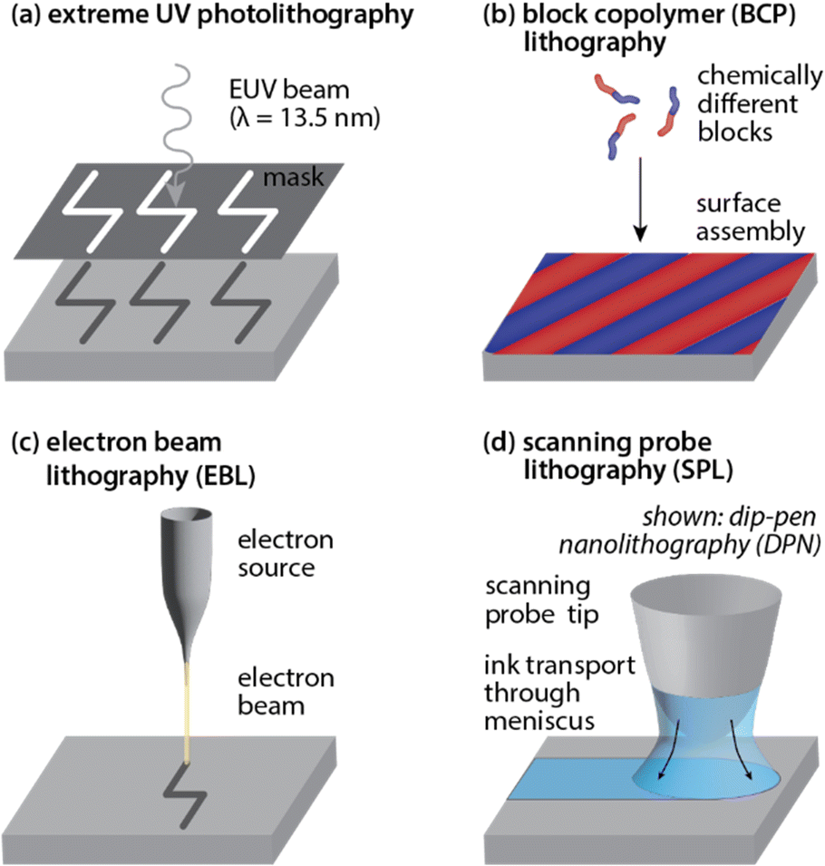 | ||
| Fig. 1 Overview of a selection of high-resolution interface patterning methods: (a) extreme UV photolithography, (b) block copolymer lithography, (c) electron-beam lithography, and (d) scanning probe lithography. | ||
![[thin space (1/6-em)]](https://www.rsc.org/images/entities/char_2009.gif) 000) for parallel printing.50 In even more highly parallelized approaches (in some cases >10 million tips) softer polymer tips are often utilized to allow for simultaneous contact with hard substrates that exhibit imperfect surface topographies.51
000) for parallel printing.50 In even more highly parallelized approaches (in some cases >10 million tips) softer polymer tips are often utilized to allow for simultaneous contact with hard substrates that exhibit imperfect surface topographies.51
Patterning of soft surfaces
Several of the methods discussed above have also been used to chemically pattern soft surfaces (e.g. hydrogels) including photo-immobilization, inkjet printing, microfluidics, and μCP;11 in some cases, physical patterning (e.g. based on wrinkling instabilities) is also possible.52,53 While techniques such as inkjet printing that operate in the 20–50 μm size regime can produce similar feature sizes for both hard and soft surfaces, for high-resolution techniques, typical feature sizes on soft substrates are substantially larger than for the same technique applied on flat crystalline surfaces. In part, this is due to topographical and chemical heterogeneity of the substrate. Many soft materials based on polymers (e.g. PDMS, hydrogels) have pores, which may range in size from less than 10 nm to greater than 1000 nm, depending on the material. Thus, patterning below the length scale of heterogeneity in the material is often challenging. | ||
| Fig. 2 Typical feature sizes on soft substrates (a) nanoscale patterns of maleimide–PEG and biotin–PEG. (b) ACRL–PEG–RGDS patterns on PEGDA hydrogels (c) fibronectin (20 μm in width) patterned on gelatin hydrogels. Adapted from ref. 54, 57, and 35, with permission. Copyright 2009 American Chemical Society, 2006 Elsevier, and 2011 Royal Society of Chemistry, respectively. | ||
Chemical patterning of hard materials with self-assembled molecular networks: 1 nm features with diverse chemistry
Most broadly utilized molecule-based patterning approaches for hard materials use standing phases of alkanethiols on gold or glass substrates; however, self-assembled molecular networks (common on 2D materials) represent an underutilized and potentially transformative means to generate useful sub-10 nm chemical patterns on both hard and soft materials. Molecular network assembly on highly oriented pyrolytic graphite (HOPG), and in some cases on other 2D materials (e.g. graphene, MoS2, WS2, black phosphorus), takes advantage of weaker molecule–substrate interactions and directional molecule–molecule interactions which allow for long-range molecular ordering based on the local flatness of the substrate.68,69 Together, these aspects of assembly enable diverse chemistries and symmetries to be designed into molecular patterns with 1 nm-resolution features, well below scales that can be easily achieved in conventional standing phase monolayer chemistries on gold. Here, we discuss this chemical patterning strategy, with a focus on patterning using striped phases of polymerizable alkyldiacetylenes, since this strategy has proven extensible to high-resolution patterning of soft surfaces.High-resolution chemical patterning based on molecular assembly on HOPG has its roots in early experimental observations in the lubrication community, which showed long-chain hydrocarbons have large enthalpies of adsorption on cast iron (containing as little as 1% carbon impurities), as well as on graphite, MoS2, and WS2.70,71 Models developed by 1970 suggested that, in the case of graphite, this might be in part due to lattice matching between the hexagonal graphite lattice (center-to-center distance 2.46 Å) and the zig-zag structure of the alkyl backbone (2.56 Å).72 With the development of scanning probe microscopy, Rabe73 and others74,75 began to observe that long-chain alkanes not only adsorbed with their chains parallel to the interface, but could form ordered linear patterns (also referred to as lamellar or striped phases) oriented in epitaxy with the HOPG lattice (Fig. 3).
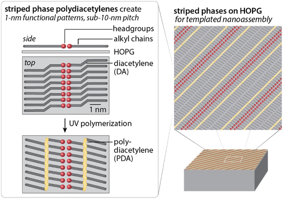 | ||
| Fig. 3 Schematic of striped-phase assembly on HOPG to generate 1 nm-resolution chemical patterns with sub-10 nm pitch, and PDA polymerization to set the chemical pattern. Adapted from ref. 121 with permission. Copyright 2021 John Wiley and Sons. | ||
Striped phase assembly of functional alkanes results in ordering of the functional headgroups into 1 nm-resolution patterns with a pitch (ca. 5–10 nm) determined by the length of the alkyl chain.74,75 Many types of functional headgroups can be embedded in such monolayers to act as nanometer-scale patterning elements, and can contribute to molecular ordering and pattern symmetry. For instance, H-bonding headgroups (e.g. carboxylic acids, amines, alcohols)74,75 can induce directional pairing at the lamellar periphery, reorienting alkyl chains relative to the lamellar axis. Conversely, molecules with functional headgroups that are wider than the alkyl backbone can locally alter lateral alkyl chain packing distances, in some cases leading to interdigitated alkyl chain structures that halve the lamellar width.
Pattern symmetry can be modified in a number of ways, including by appending functional moieties and/or alkyl chains to an aromatic core, diversifying the functional patterns that can be installed at the interface.68,76–80 Directional interactions can be achieved through H-bonding,81 halogen bonding,82,83 or dipole–dipole interactions,84,85 as well as metal coordination. Binary and in some cases higher-order molecular patterns can also be used to establish additional pattern complexity.81
Functional patterns established through self-assembled molecular networks are typically non-covalently adsorbed to the substrate. In some cases, pattern stability can be increased using reactions that introduce covalent bonds between pattern elements (e.g. polydiacetylene photopolymerization,86,87 thiophene polymerization,88 Ullman coupling,89,90 boronic acid polycondensation91–94). For instance, functional alkanes with embedded diacetylene groups can undergo topochemical photopolymerization to generate a conjugated polydiacetylene (PDA) backbone86 that links molecules over tens to hundreds of nanometers. Attractive aspects of this reaction include the photoactivation, which enables it to be carried out without the introduction of additional solvents or reactions following pattern formation. Additionally, the polymerization reactions have been well-studied in 3D crystals and in Langmuir films,95–100 with the result that a small range of appropriate monomers are commercially available. Of these, 10,12-diynoic acids such as 10,12-pentacosadiynoic acid (PCDA) have been the most broadly studied using scanning tunneling microscopy (STM), by the groups of Okawa and others.87,101–104 In the context of STM studies, polymerization can be carried out not only with UV irradiation, but also by using tunneling electrons from the STM tip, generating individual conjugated PDAs that have been studied with an interest in molecular electronics.
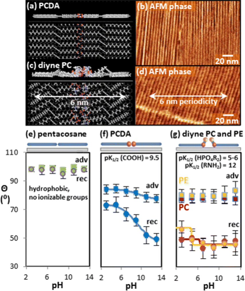 | ||
| Fig. 4 (a) Molecular model and (b) AFM image of PCDA/HOPG striped phase, and (c) model and (d) AFM image of diyne PC/HOPG striped phase. (e–g) Contact angle titrations for (e) pentacosane, (f) PCDA, and (g) diyne PC and diyne PE. Adapted from ref. 105 with permission. Copyright 2016 American Chemical Society. | ||
We have also found that it is possible to use microcontact printing (μCP) to generate microscale geometric patterns (e.g. squares, Fig. 5) comprised of nm-wide chemical stripes,112 including amphiphiles with complex headgroup chemistries (e.g., phosphoinositol, a phospholipid that incorporates an inositol carbohydrate in the headgroup). To generate additional chemical complexity, striped patterns of amphiphiles can also act as displaceable templates, controlling assembly of complex molecules (e.g., end-functionalized diphenylalanine (FF) peptides) by controlling access to the aromatic substrate on the scale of the assembling molecule footprint.113
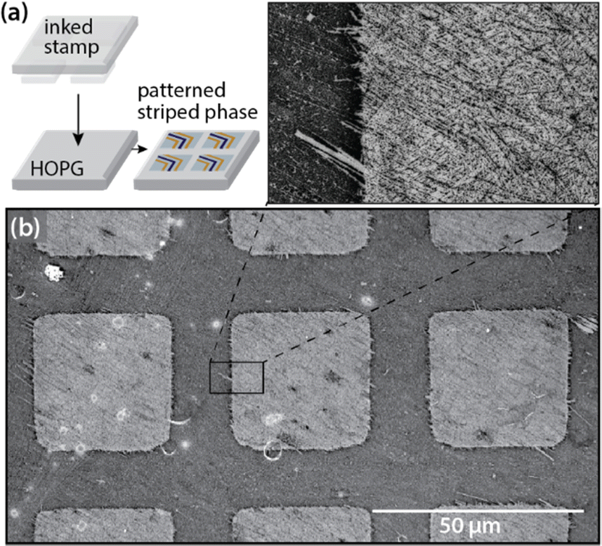 | ||
| Fig. 5 (a) Schematic of microcontact printing of striped phases on HOPG with geometric control. (b) SEM image of microcontact printed patterns of striped PDAs (sPDAs) on HOPG. Adapted from ref. 113 with permission. Copyright 2020 American Chemical Society. | ||
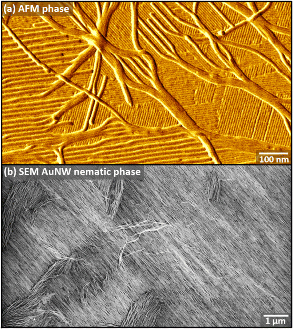 | ||
| Fig. 6 (a) AFM phase image of AuNWs adsorbed to a phospholipid sPDA with small domains, illustrating differences in wire assembly when misaligned vs. aligned with the sPDA lamellar axis. (b) SEM images of AuNWs assembled on dPE sPDA with long-range order. Adapted from ref. 116 with permission. Copyright 2019 Cell Press. | ||
We observed that striped molecular patterns with strong dipoles in the headgroups (e.g. phosphoethanolamine) were capable of orienting and ordering ultranarrow gold nanowires (AuNWs), pointing to the importance of specific chemistries embedded in these functional patterns.116 High-resolution AFM images illustrate that when wires are aligned with the striped template, they separate to distances up to 30 nm (Fig. 6a), with highly aligned arrays of AuNWs achieved over areas of many μm2 (Fig. 6b).117–119 Overall, these findings point to a potentially broad-impact design principle: polar functional groups common in biology can impact their environment over much greater distances in nonpolar solvents common in synthetic materials.
Chemical patterning of soft surfaces with lying-down monolayers
Most classical surface science approaches to achieving precise molecular order and functionalization rely on atomic order in the substrate lattice to achieve ordering of molecules that adsorb to the surface. However, many emerging materials applications, particularly those that interface with biology, utilize amorphous soft materials with heterogeneous surfaces. This raises significant challenges in precise control of surfaces for wearable electronics and cell culture, for example, to control ligand clustering for interactions with cells; as mentioned earlier, most patterning methods (e.g., EBL, photolithography) that are useful on hard surfaces provide decreased resolution on soft materials.Recently, we have found that it is possible to assemble molecular networks with embedded 1 nm-resolution functional patterns on HOPG, polymerize to set the functional pattern, then transfer polymerized striped phases from HOPG to other materials (Fig. 7), taking advantage of the sPDA backbone as a scaffold to stabilize the nm-scale chemical patterns during transfer.12,13 Transfer is achieved using reactions (e.g. hydrosilylation or acrylate radical-mediated polymerization) that form covalent links to the sPDA polymer backbones in the monolayer molecular network.
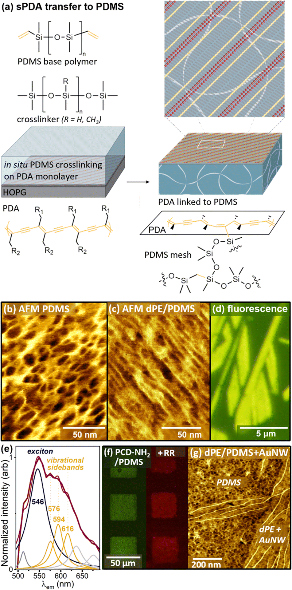 | ||
| Fig. 7 (a) Schematic of sPDA transfer from HOPG to PDMS. (b,c) AFM images of (b) unfunctionalized PDMS, and (c) PDMS with transferred dPE sPDA layer. (d) Fluorescence micrograph of dPE transferred to PDMS. (e) Fluorescence emission spectrum of dPE/PDMS. (f) Fluorescence micrographs of PCD-NH2 sPDAs on PDMS as-transferred (left) and after reaction with derivatized rhodamine red (right). (g) AuNWs adsorb only in sPDA-functionalized regions of PDMS, recapitulating assembly behavior on sPDAs on HOPG. Adapted from ref. 12 with permission. Copyright 2021 American Chemical Society. | ||
Transfer of sPDAs to PDMS (Fig. 7a), takes advantage of the PDMS crosslinking reaction, which is carried out in situ, with the liquid PDMS reaction mixture in contact with the sPDA. PDMS crosslinking typically involves covalent bond formation between Si–H groups in the PDMS crosslinker and vinyl groups in the PDMS base polymer, in the presence of a transition metal catalyst. When carried out in contact with an sPDA monolayer, crosslinks are also formed with the PDA backbone. After curing, exfoliation of the PDMS from the HOPG also removes sPDAs covalently linked to the PDMS surface. After transfer, the monolayer is visible at small scales in AFM images. Fig. 7b shows unfunctionalized SYLGARD 184 PDMS, with a mesh size of approximately 10 nm. Fig. 7c shows the same PDMS blend cured in contact with dPE/HOPG as shown in Fig. 7a; here, linear features are visible along the PDMS surface. At larger scales, transfer can be characterized based on fluorescence emission from the sPDA backbones (Fig. 7d and e). Following transfer, the monolayer headgroup chemistry can be utilized for post-functionalization or further assembly (e.g. with rhodamine derivatives, Fig. 7f, assembly of AuNWs, Fig. 7g, or controlled adsorption of oppositely-charged electrolytes).12,120
Characterizing chemistry at soft, porous interfaces is an ongoing challenge; however, the sPDA transfer approach benefits from the ability to readily extract information regarding nm-scale interface structure on HOPG prior to transfer, and correlate with interface properties on the soft material after transfer.121,122 For instance, individual polymerization events on HOPG can be characterized by AFM, based on Å-scale topographical protrusion of the sPDA backbone following polymerization. Correlating nanoscale extent of polymerization on HOPG (Fig. 8a, main images) with microscale sPDA transfer (quantified through sPDA fluorescence emission, Fig. 8a, insets) enables a multiscale view of the polymerization process. Already, this approach has allowed us to identify a large and previously unreported difference in polymerization efficiency between the two most common commercially available monomers for striped phases, PCDA (referred to here as PCD-COOH for clear comparison with PCD-NH2) and tricosadiynoic acid (TCD–COOH) (Fig. 8b, dotted grey lines), enabling design new high-efficiency monomers for polymerization and surface functionalization of PDMS.
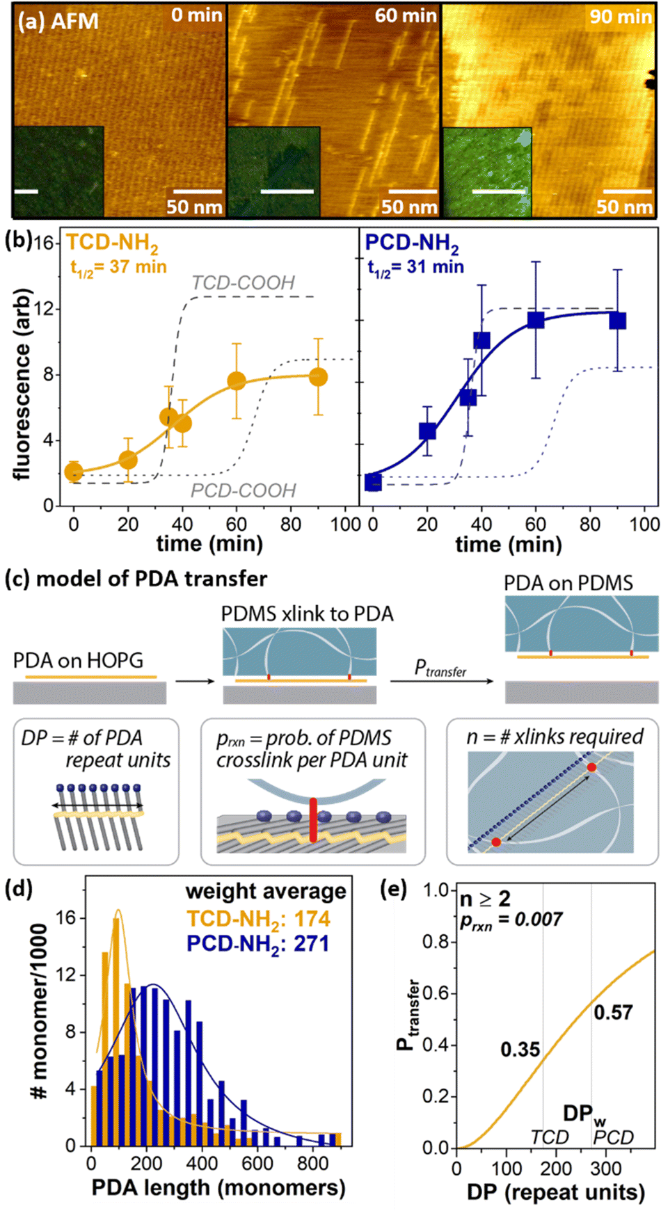 | ||
| Fig. 8 (a) AFM and fluorescence characterization of PCD–COOH polymerization at 0 min, 60 min, and 90 min, illustrating that fluorescence intensity of material transferred to PDMS increases with the extent of polymerization on HOPG. (b) Fluorescence of TCD-NH2 (left) and PCD-NH2 (right) transferred to PDMS after different periods of UV polymerization on HOPG. Dotted lines illustrate comparison with structurally analogous carboxylic acids. (c) Probabilistic model describing sPDA transfer to PDMS. (d) Histogram of weight average degree of polymerization for TCD-NH2 and PCD-NH2 on HOPG. (e) Calculated fractional transfer for TCD-NH2 and PCD-NH2, based on model and on experimentally observed populations of polymer lengths. Adapted from ref. 121 and 122 with permission. Copyright 2021 John Wiley and Sons, and 2022 American Chemical Society, respectively. | ||
More recently, we have extended this understanding to the transfer of molecules with different headgroup chemistries, such as amines (Fig. 8b, blue and gold lines). The ability to quantify lengths of large populations of individual polymers on HOPG has allowed us to develop models of sPDA transfer to PDMS that relate the degree of polymerization (DP), probability of crosslinking per PDA unit (prxn), and the number of crosslinks required for sPDA exfoliation (n), as illustrated in Fig. 8c. Overall, these models point to the likelihood that at least 2 crosslinks are required for PDA exfoliation, with prxn in the range of 1–3% per PDA unit (Fig. 8e).
While PDMS is broadly used for many applications including microfluidics, other classes of more hydrophilic polymers (e.g. hydrogels) are more commonly used in applications that require direct contact with biological environments. We have discovered that a similar in situ polymerization process enables sPDA transfer to acrylate hydrogels (Fig. 9a),13 with transfer dependent upon gel composition (Fig. 9b). The transferred PDA layer is also visible in cryoelectron microscopy, altering surface pore structure (Fig. 9c, main image) in comparison with unfunctionalized polyacrylamide (PAAm, Fig. 9c, inset). When amine PDA layers are transferred to the hydrogel surface, they template adsorption of charged electrolytes such as DNA (molecular model, Fig. 9d, experimental data, Fig. 9e and f). More broadly, these findings may point to utility of sPDA monolayers in structuring multivalent binding interactions with analytes in the environment.
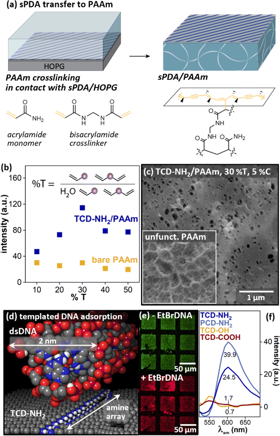 | ||
| Fig. 9 (a) Schematic of sPDA transfer from HOPG to PAAm. (b) sPDA fluorescence emission with varying PAAm composition. (c) Cryoelectron microscopy of functionalized and unfunctionalized PAAm, illustrating difference in pore structure. (d) Molecular model of dsDNA and TCD-NH2, illustrating relative size scales of functional patterns. (e) Microcontact patterned TCD-NH2/PAAm without (top) and with (bottom) exposure to EtBr-labeled dsDNA. (f) Fluorescence emission from amine, hydroxyl, and carboxylic-acid functionalized PAAm surfaces after exposure to EtBr–DNA, illustrating impact of amine functional group on dsDNA adsorption. Adapted from ref. 13 with permission. Copyright 2022 American Chemical Society. | ||
Outlook
While much of the work on high-resolution surface patterning to date has focused on hard, often crystalline, surfaces, there is a growing need for methods that enable scalable, high-resolution patterning of soft materials for interfaces with biology. A number of studies have illustrated that direct translation of methods that are effective in patterning hard materials produce much larger feature sizes in soft materials.We suggest that self-assembled molecular networks and other similar chemical patterning strategies represent a powerful and underutilized toolkit for high-resolution chemical control of soft interfaces. In particular, molecular networks that allow for on-surface reactivity enable patterns to be assembled on hard, crystalline materials, covalently locked, and then transferred to soft materials, as long as the polymerized pattern has total dimensions that exceed the scale of surface defects (e.g. pores) in the soft material. Here, we have focused on a class of chemical patterns based on polydiacetylenes, in which the polydiacetylene backbone itself acts as a structural integrity element, and as an optical readout of transfer. More broadly, given the resurgence of interest in on-surface reactions in relation to catalysis and other applications, there are likely to be a wide range of structural motifs that exhibit similar behavior.
We note that integration of high-resolution patterning strategies with soft materials creates a parallel need for high-resolution interfacial characterization strategies that work well at such material interfaces. Many high-resolution interfacial characterization methods to date depend on an intersection of material properties (e.g. conductivity) that exclude soft materials such as hydrogels. Techniques such as super-resolution optical microscopy that operate on soft materials typically require complex fluorescent labels, complicating interface design. Again, because on-surface molecular assembly and reaction pathways have often focused on materials that embed conjugated bond networks, for molecular electronics and other applications, there are likely to be many classes of materials that provide useful optical readouts of transfer.
Author contributions
A. S., A. S. and S. A. C. wrote the manuscript. S. A. C. edited the manuscript.Conflicts of interest
There are no conflicts to declare.Acknowledgements
S. A. C. Acknowledges support through an NSF grant, NSF-CHE-MSN 2108966.Notes and references
- Y. Q. Chen, Z. W. Shu, S. Zhang, P. Zeng, H. K. Liang, M. J. Zheng and H. G. Duan, Sub-10 nm Fabrication: Methods and Applications, Int. J. Extreme Manuf., 2021, 3, 032002 CrossRef CAS.
- S. V. Graeter, J. H. Huang, N. Perschmann, M. Lopez-Garcia, H. Kessler, J. D. Ding and J. P. Spatz, Mimicking Cellular Environments by Nanostructured Soft Interfaces, Nano Lett., 2007, 7, 1413–1418 CrossRef CAS.
- M. Kremer, E. Pothmann, T. Rossler, J. Baker, A. Yee, H. Blach and J. M. Prausnitz, Pore-Size Distributions of Cationic Polyacrylamide Hydrogels Varying in Initial Monomer Concentration and Cross-Linker/Monomer Ratio, Macromolecules, 1994, 27, 2965–2973 CrossRef CAS.
- N. Weiss and A. Silberberg, Inhomogeneity of Polyacrylamide Gel Structure from Permeability and Viscoelasticity, Br. Polym. J., 1977, 9, 144–150 CrossRef CAS.
- N. Annabi, J. W. Nichol, X. Zhong, C. Ji, S. Koshy, A. Khademhosseini and F. Dehghani, Controlling the Porosity and Microarchitecture of Hydrogels for Tissue Engineering, Tissue Eng., Part B, 2010, 16, 371–383 CrossRef CAS.
- L. Capodieci, From Optical Proximity Correction to Lithography-Driven Physical Design (1996–2006): 10 Years of Resolution Enhancement Technology and the Roadmap Enablers for the Next Decade. Proc. SPIE: Opt. Microlithog. XIX 2006, 6154, 615401.
- J. E. E. Baglin, Ion Beam Nanoscale Fabrication and Lithography—a Review, Appl. Surf. Sci., 2012, 258, 4103–4111 CrossRef CAS.
- F. S. Bates, M. A. Hillmyer, T. P. Lodge, C. M. Bates, K. T. Delaney and G. H. Fredrickson, Multiblock Polymers: Panacea or Pandora's Box?, Science, 2012, 336, 434–440 CrossRef CAS.
- A. Kumar, H. A. Biebuyck and G. M. Whitesides, Patterning Self-Assembled Monolayers: Applications in Materials Science, Langmuir, 1994, 10, 1498–1511 CrossRef CAS.
- S. A. Claridge, W.-S. Liao, J. C. Thomas, Y. Zhao, H. H. Cao, S. Cheunkar, A. C. Serino, A. M. Andrews and P. S. Weiss, From the Bottom Up: Dimensional Control and Characterization in Molecular Monolayers, Chem. Soc. Rev., 2013, 42, 2725–2745 RSC.
- B. G. Munoz-Robles, I. Kopyeva and C. A. DeForest, Surface Patterning of Hydrogel Biomaterials to Probe and Direct Cell-Matrix Interactions, Adv. Mater. Interfaces, 2020, 7, 2001198 CrossRef CAS.
- T. C. Davis, J. O. Bechtold, A. Shi, E. N. Lang, A. Singh and S. A. Claridge, One Nanometer Wide Functional Patterns with a Sub-10 Nanometer Pitch Transferred to an Amorphous Elastomeric Material, ACS Nano, 2021, 15, 1426–1435 CrossRef CAS PubMed.
- J. C. Arango, L. O. Williams, A. Shi, A. Singh, E. K. Nava, R. V. Fisher, J. A. Garfield and S. A. Claridge, Nanostructured Surface Functionalization of Polyacrylamide Hydrogels Below the Length Scale of Hydrogel Heterogeneity, ACS Appl. Mater. Interfaces, 2022, 14(38), 43937–43945 CrossRef CAS.
- C. G. Willson, R. R. Dammel and A. Reiser, Photoresist Materials: A Historical Perspective, Proc. SPIE: Adv. Resist Technol. Proc. XIV, 1997, 3049, 275826 Search PubMed.
- G. J. Leggett, Photolithography Beyond the Diffraction Limit, in Nanolithography and Patterning Techniques in Microelectronics, D. Bucknell ed. Elsevier, 2005, pp. 238–266 Search PubMed.
- D. Fan and Y. Ekinci, Photolithography Reaches 6 nm Half-Pitch Using EUV Light, Proc. SPIE, 2016, 9776, 97761V CrossRef.
- V. Bakshi, EUV Lithography, SPIE Press, 2009 Search PubMed.
- J. Garofalo, C. J. Biddick, R. L. Kostelak and S. Vaidya, Mask Assisted Off-Axis Illumination Technique for Random Logic, J. Vac. Sci. Technol., B, 1993, 11, 2651–2658 CrossRef.
- M. D. Levenson, N. S. Viswanathan and R. A. Simpson, Improving Resolution in Photolithography with a Phase-Shifting Mask, IEEE Trans. Electron. Devices, 1982, 29, 1828–1836 Search PubMed.
- V. R. Manfrinato, L. H. Zhang, D. Su, H. G. Duan, R. G. Hobbs, E. A. Stach and K. K. Berggren, Resolution Limits of Electron-Beam Lithography toward the Atomic Scale, Nano Lett., 2013, 13, 1555–1558 CrossRef CAS PubMed.
- A. E. Grigorescu and C. W. Hagen, Resists for Sub-20 nm Electron Beam Lithography with a Focus on HSQ: State of the Art, Nanotechnology, 2009, 20, 292001 CrossRef CAS PubMed.
- A. A. Tseng, K. Chen, C. D. Chen and K. J. Ma, Electron Beam Lithography in Nanoscale Fabrication: Recent Developments, IEEE Trans. Electron Devices, 2003, 26, 141–149 CAS.
- J. Orloff, Fundamental Limits to Imaging Resolution for Focused Ion Beams, J. Vac. Sci. Technol., B: Microelectron. Nanometer Struct.--Process., Meas., Phenom., 1996, 14, 3759–3763 CrossRef CAS.
- K. Li, J. Li, C. Reardon, C. S. Schuster, Y. Wang, G. J. Triggs, N. Damnik, J. Muenchenberger, X. Wang, E. R. Martins and T. F. Krauss, High Speed E-Beam Writing for Large Area Photonic Nanostructures - a Choice of Parameters, Sci. Rep., 2016, 6, 32945 CrossRef CAS.
- C. M. Bates, M. J. Maher, D. W. Janes, C. J. Ellison and C. G. Willson, Block Copolymer Lithography, Macromolecules, 2014, 47, 2–12 CrossRef CAS.
- W. J. Durand, G. Blachut, M. J. Maher, S. Sirard, S. Tein, M. C. Carlson, Y. Asano, S. X. Zhou, A. P. Lane, C. M. Bates, C. J. Ellison and C. G. Willson, Design of High-Chi Block Copolymers for Lithography, J. Polym. Sci., Part A: Polym. Chem., 2015, 53, 344–352 CrossRef CAS.
- C. M. Bates, T. Seshimo, M. J. Maher, W. J. Durand, J. D. Cushen, L. M. Dean, G. Blachut, C. J. Ellison and C. G. Willson, Polarity-Switching Top Coats Enable Orientation of Sub-10 nm Block Copolymer Domains, Science, 2012, 338, 775–779 CrossRef CAS.
- J. G. Kennemur, L. Yao, F. S. Bates and M. A. Hillmyer, Sub-5 nm Domains in Ordered Poly(Cyclohexylethylene)-Block-Poly(Methyl Methacrylate) Block Polymers for Lithography, Macromolecules, 2014, 47, 1411–1418 CrossRef CAS.
- G. G. Yang, H. J. Choi, K. H. Han, J. H. Kim, C. W. Lee, E. I. Jung, H. M. Jin and S. O. Kim, Block Copolymer Nanopatterning for Nonsemiconductor Device Applications, ACS Appl. Mater. Interface, 2022, 14, 12011–12037 CrossRef CAS PubMed.
- M. Park, C. Harrison, P. M. Chaikin, R. A. Register and D. H. Adamson, Block Copolymer Lithography: Periodic Arrays of ∼10^11 Holes in 1 Square Centimeter, Science, 1997, 276, 1401–1404 CrossRef CAS.
- M. P. Stoykovich, H. Kang, K. C. Daoulas, G. S. Liu, C. C. Liu, J. J. de Pablo, M. Muller and P. F. Nealey, Directed Self-Assembly of Block Copolymers for Nanolithography: Fabrication of Isolated Features and Essential Integrated Circuit Geometries, ACS Nano, 2007, 1, 168–175 CrossRef CAS.
- B. Stel, I. Gunkel, X. Gu, T. P. Russell, J. J. De Yoreo and M. Lingenfelder, Contrasting Chemistry of Block Copolymer Films Controls the Dynamics of Protein Self-Assembly at the Nanoscale, ACS Nano, 2019, 13, 4018–4027 CrossRef CAS PubMed.
- A. Kumar and G. M. Whitesides, Features of Gold Having Micrometer to Centimeter Dimensions Can Be Formed through a Combination of Stamping with an Elastomeric Stamp and an Alkanethiol Ink Followed by Chemical Etching, Appl. Phys. Lett., 1993, 63, 2002–2004 CrossRef CAS.
- A. Kumar, H. A. Biebuyck and G. M. Whitesides, Patterning Self-Assembled Monolayers - Applications in Materials Science, Langmuir, 1994, 10, 1498–1511 CrossRef CAS.
- A. G. Castaño, V. Hortiguela, A. Lagunas, C. Cortina, N. Montserrat, J. Samitier and E. Martinez, Protein Patterning on Hydrogels by Direct Microcontact Printing: Application to Cardiac Differentiation, RSC Adv., 2014, 4, 29120–29123 RSC.
- E. Delamarche, H. Schmid, A. Bietsch, N. B. Larsen, H. Rothuizen, B. Michel and H. Biebuyck, Transport Mechanisms of Alkanethiols During Microcontact Printing on Gold, J. Phys. Chem. B, 1998, 102, 3324–3334 CrossRef CAS.
- H.-W. Li, B. V. O. Muir, G. Fichet and W. T. S. Huck, Nanocontact Printing: A Route to Sub-50 nm-Scale Chemical and Biological Patterning, Langmuir, 2003, 19, 1963–1965 CrossRef CAS.
- W. S. Liao, S. Cheunkar, H. H. Cao, H. R. Bednar, P. S. Weiss and A. M. Andrews, Subtractive Patterning Via Chemical Lift-Off Lithography, Science, 2012, 337, 1517–1521 CrossRef CAS.
- C. Y. Chen, C. M. Wang and W. S. Liao, A Special Connection between Nanofabrication and Analytical Devices: Chemical Lift-Off Lithography, Bull. Chem. Soc. Jpn., 2019, 92, 600–607 CrossRef CAS.
- C. Y. Chen, C. M. Wang, H. H. Li, H. H. Chan and W. S. Liao, Wafer-Scale Bioactive Substrate Patterning by Chemical Lift-Off Lithography, Beilstein J. Nanotechnol., 2018, 9, 311–320 CrossRef CAS.
- S. Y. Chou, P. R. Krauss and P. J. Renstrom, Imprint Lithography with 25-Nanometer Resolution, Science, 1996, 272, 85–87 CrossRef CAS.
- G. Y. Liu, S. Xu and Y. L. Qian, Nanofabrication of Self-Assembled Monolayers Using Scanning Probe Lithography, Acc. Chem. Res., 2000, 33, 457–466 CrossRef CAS.
- R. Garcia, A. W. Knoll and E. Riedo, Advanced Scanning Probe Lithography, Nat. Nanotechnol., 2014, 9, 577–587 CrossRef CAS PubMed.
- G. Q. Liu, S. H. Petrosko, Z. J. Zheng and C. A. Mirkin, Evolution of Dip-Pen Nanolithography (DPN): From Molecular Patterning to Materials Discovery, Chem. Rev., 2020, 120, 6009–6047 CrossRef CAS PubMed.
- R. D. Piner, J. Zhu, F. Xu, S. H. Hong and C. A. Mirkin, “Dip-Pen” Nanolithography, Science, 1999, 283, 661–663 CrossRef CAS PubMed.
- A. Urtizberea, M. Hirtz and H. Fuchs, Ink Transport Modelling in Dip-Pen Nanolithography and Polymer Pen Lithography, Nanofabrication, 2016, 2, 43–53 Search PubMed.
- K. A. Brown, D. J. Eichelsdoerfer, X. Liao, S. He and C. A. Mirkin, Material Transport in Dip-Pen Nanolithography, Front. Phys., 2014, 9, 385–397 CrossRef.
- J. Jang, G. C. Schatz and M. A. Ratner, Capillary Force on a Nanoscale Tip in Dip-Pen Nanolithography, Phys. Rev. Lett., 2003, 90, 156104 CrossRef PubMed.
- A. B. Braunschweig, F. Huo and C. A. Mirkin, Molecular Printing, Nat. Chem., 2009, 1, 353–358 CrossRef CAS.
- K. Salaita, Y. Wang, J. Fragala, R. A. Vega, C. Liu and C. A. Mirkin, Massively Parallel Dip-Pen Nanolithography with 55000-Pen Two-Dimensional Arrays, Angew. Chem., 2006, 45, 7220–7223 CrossRef CAS PubMed.
- F. Huo, Z. Zheng, G. Zheng, L. R. Giam, H. Zhang and C. A. Mirkin, Polymer Pen Lithography, Science, 2008, 321, 1658–1660 CrossRef CAS PubMed.
- E. P. Chan and A. J. Crosby, Spontaneous Formation of Stable Aligned Wrinkling Patterns, Soft Matter, 2006, 2, 324–328 RSC.
- N. Bowden, S. Brittain, A. G. Evans, J. W. Hutchinson and G. M. Whitesides, Spontaneous Formation of Ordered Structures in Thin Films of Metals Supported on an Elastomeric Polymer, Nature, 1998, 393, 146–149 CrossRef CAS.
- C. M. Kolodziej and H. D. Maynard, Electron-Beam Lithography for Patterning Biomolecules at the Micron and Nanometer Scale, Chem. Mater., 2011, 24, 774–780 CrossRef.
- K. L. Christman, E. Schopf, R. M. Broyer, R. C. Li, Y. Chen and H. D. Maynard, Positioning Multiple Proteins at the Nanoscale with Electron Beam Cross-Linked Functional Polymers, J. Am. Chem. Soc., 2009, 131, 521–527 CrossRef CAS PubMed.
- V. R. Tirumala, R. Divan, L. E. Ocola and D. C. Mancini, Direct-Write E-Beam Patterning of Stimuli-Responsive Hydrogel Nanostructures, J. Vac. Sci. Technol., B: Microelectron. Nanometer Struct.--Process., Meas., Phenom., 2005, 23, 3124 CrossRef CAS.
- M. S. Hahn, J. S. Miller and J. L. West, Laser Scanning Lithography for Surface Micropatterning on Hydrogels, Adv. Mater., 2005, 17, 2939–2942 CrossRef CAS.
- M. S. Hahn, J. S. Miller and J. L. West, Three-Dimensional Biochemical and Biomechanical Patterning of Hydrogels for Guiding Cell Behavior, Adv. Mater., 2006, 18, 2679–2684 CrossRef CAS.
- M. S. Hahn, L. J. Taite, J. J. Moon, M. C. Rowland, K. A. Ruffino and J. L. West, Photolithographic Patterning of Poyethylene Glycol Hydrogels, Biomaterials, 2006, 27, 2519–2524 CrossRef CAS PubMed.
- I. Batalov, K. R. Stevens and C. A. DeForest, Photopatterned Biomolecule Immobilization to Guide Three-Dimensional Cell Fate in Natural Protein-Based Hydrogels, Proc. Natl. Acad. Sci. U. S. A., 2021, 118, e2014194118 CrossRef CAS PubMed.
- C. A. DeForest, B. D. Polizzotti and K. S. Anseth, Sequential Click Reactions for Synthesizing and Patterning Three-Dimensional Cell Microenvironments, Nat. Mater., 2009, 8, 659–664 CrossRef CAS PubMed.
- C. A. DeForest and K. S. Anseth, Cytocompatible Click-Based Hydrogels with Dynamically Tunable Properties through Orthogonal Photoconjugation and Photocleavage Reactions, Nat. Chem., 2011, 3, 925–931 CrossRef CAS PubMed.
- C. A. DeForest, E. A. Sims and K. S. Anseth, Peptide-Functionalized Click Hydrogels with Independently Tunable Mechanics and Chemical Functionality for 3D Cell Culture, Chem. Mater., 2010, 22, 4783–4790 CrossRef CAS PubMed.
- F. Guilak, D. M. Cohen, B. T. Estes, J. M. Gimble, W. Liedtke and C. S. Chen, Control of Stem Cell Fate by Physical Interactions with the Extracellular Matrix, Cell Stem Cell, 2009, 5, 17–26 CrossRef CAS PubMed.
- S. Raghavan and C. S. Chen, Micropatterned Environments in Cell Biology, Adv. Mater., 2004, 16, 1303–1313 CrossRef CAS.
- R. McBeath, D. M. Pirone, C. M. Nelson, K. Bhadriraju and C. S. Chen, Cell Shape, Cytoskeletal Tension, and RhoA Regulate Stem Cell Lineage Commitment, Dev. Cell, 2004, 6, 483–495 CrossRef CAS PubMed.
- M. R. Burnham, J. N. Turner, D. Szarowski and D. L. Martin, Biological Functionalization and Surface Micropatterning of Polyacrylamide Hydrogels, Biomaterials, 2006, 27, 5883–5891 CrossRef CAS PubMed.
- D. P. Goronzy, M. Ebrahimi, F. Rosei, Arramel, Y. Fang, S. De Feyter, S. L. Tait, C. Wang, P. H. Beton, A. T. S. Wee, P. S. Weiss and D. F. Perepichka, Supramolecular Assemblies on Surfaces: Nanopatterning, Functionality, and Reactivity, ACS Nano, 2018, 12, 7445–7481 CrossRef CAS PubMed.
- A. Shi and S. A. Claridge, Lipids: An Atomic Toolkit for the Endless Frontier, ACS Nano, 2021, 15, 15429–15445 CrossRef CAS PubMed.
- A. J. Groszek, Preferential Adsorption of Normal Hydrocarbons on Cast Iron, Nature, 1962, 196, 531–533 CrossRef CAS.
- A. J. Groszek, Preferential Adsorption of Long-Chain Normal Paraffins on MoS2, WS2 and Graphite from N-Heptane, Nature, 1964, 204, 680 CrossRef CAS.
- A. J. Groszek, Selective Adsorption at Graphite/Hydrocarbon Interfaces, Proc. R. Soc. London, Ser. A, 1970, 314, 473 Search PubMed.
- J. P. Rabe and S. Buchholz, Commensurability and Mobility in 2-Dimensional Molecular Patterns on Graphite, Science, 1991, 253, 424–427 CrossRef CAS PubMed.
- D. M. Cyr, B. Venkataraman and G. W. Flynn, STM Investigations of Organic Molecules Physisorbed at the Liquid-Solid Interface, Chem. Mater., 1996, 8, 1600–1615 CrossRef CAS.
- D. M. Cyr, B. Venkataraman, G. W. Flynn, A. Black and G. M. Whitesides, Functional Group Identification in Scanning Tunneling Microscopy of Molecular Adsorbates, J. Phys. Chem., 1996, 100, 13747–13759 CrossRef CAS.
- S. De Feyter and F. C. De Schryver, Self-Assembly at the Liquid/Solid Interface: STM Reveals, J. Phys. Chem. B, 2005, 109, 4290–4302 CrossRef CAS PubMed.
- J. M. MacLeod and F. Rosei, Molecular Self-Assembly on Graphene, Small, 2014, 10, 1038–1049 CrossRef CAS PubMed.
- J. A. Mann and W. R. Dichtel, Noncovalent Functionalization of Graphene by Molecular and Polymeric Adsorbates, J. Phys. Chem. Lett., 2013, 4, 2649–2657 CrossRef CAS.
- S. Furukawa, H. Uji-i, K. Tahara, T. Ichikawa, M. Sonoda, F. C. De Schryver, Y. Tobe and S. De Feyter, Molecular Geometry Directed Kagome and Honeycomb Networks: Toward Two-Dimensional Crystal Engineering, J. Am. Chem. Soc., 2006, 128, 3502–3503 CrossRef CAS PubMed.
- K. Tahara, S. Furukawa, H. Uji-I, T. Uchino, T. Ichikawa, J. Zhang, W. Mamdouh, M. Sonoda, F. C. De Schryver, S. De Feyter and Y. Tobe, Two-Dimensional Porous Molecular Networks of Dehydrobenzo[12]Annulene Derivatives Via Alkyl Chain Interdigitation, J. Am. Chem. Soc., 2006, 128, 16613–16625 CrossRef CAS PubMed.
- J. Liu, T. Chen, X. Deng, D. Wang, J. Pei and L.-J. Wan, Chiral Hierarchical Molecular Nanostructures on Two-Dimensional Surface by Controllable Trinary Self-Assembly, J. Am. Chem. Soc., 2011, 133, 21010–21015 CrossRef CAS PubMed.
- R. Gutzler, C. Fu, A. Dadvand, Y. Hua, J. M. MacLeod, F. Rosei and D. F. Perepichka, Halogen Bonds in 2D Supramolecular Self-Assembly of Organic Semiconductors, Nanoscale, 2012, 4, 5965–5971 RSC.
- Q.-N. Zheng, X.-H. Liu, T. Chen, H.-J. Yan, T. Cook, D. Wang, P. J. Stang and L.-J. Wan, Formation of Halogen Bond-Based 2D Supramolecular Assemblies by Electric Manipulation, J. Am. Chem. Soc., 2015, 137, 6128–6131 CrossRef CAS PubMed.
- Y. H. Wei, W. J. Tong and M. B. Zimmt, Self-Assembly of Patterned Monolayers with Nanometer Features: Molecular Selection Based on Dipole Interactions and Chain Length, J. Am. Chem. Soc., 2008, 130, 3399–3405 CrossRef CAS PubMed.
- Y. Wei, W. J. Tong, C. Wise, X. D. Wei, K. Armbrust and M. B. Zimmt, Dipolar Control of Monolayer Morphology: Spontaneous SAM Patterning, J. Am. Chem. Soc., 2006, 128, 13362–13363 CrossRef CAS PubMed.
- P. C. M. Grim, S. De Feyter, A. Gesquiere, P. Vanoppen, M. Rucker, S. Valiyaveettil, G. Moessner, K. Mullen and F. C. De Schryver, Submolecularly Resolved Polymerization of Diacetylene Molecules on the Graphite Surface Observed with Scanning Tunneling Microscopy, Angew. Chem., Int. Ed., 1997, 36, 2601–2603 CrossRef CAS.
- M. Akai-Kasaya, K. Shimizu, Y. Watanabe, A. Saito, M. Aono and Y. Kuwahara, Electronic Structure of a Polydiacetylene Nanowire Fabricated on Highly Ordered Pyrolytic Graphite, Phys. Rev. Lett., 2003, 91, 255501 CrossRef CAS PubMed.
- G. S. McCarty and P. S. Weiss, Formation and Manipulation of Protopolymer Chains, J. Am. Chem. Soc., 2004, 126, 16772–16776 CrossRef CAS PubMed.
- J. A. Lipton-Duffin, O. Ivasenko, D. F. Perepichka and F. Rosei, Synthesis of Polyphenylene Molecular Wires by Surface-Confined Polymerization, Small, 2009, 5, 592–597 CrossRef CAS PubMed.
- M. M. Blake, S. U. Nanayakkara, S. A. Claridge, L. C. Fernandez-Torres, E. C. H. Sykes and P. S. Weiss, Identifying Reactive Intermediates in the Ullmann Coupling Reaction by Scanning Tunneling Microscopy and Spectroscopy, J. Phys. Chem. A, 2009, 113, 13167–13172 CrossRef CAS PubMed.
- J. W. Colson and W. R. Dichtel, Rationally Synthesized Two-Dimensional Polymers, Nat. Chem., 2013, 5, 453–465 CrossRef CAS PubMed.
- N. A. A. Zwaneveld, R. Pawlak, M. Abel, D. Catalin, D. Gimes, D. Bertin and L. Porte, Organized Formation of 2D Extended Covalent Organic Frameworks at Surfaces, J. Am. Chem. Soc., 2008, 130, 6678–6679 CrossRef CAS PubMed.
- S. Spitzer, A. Rastgoo-Lahrood, K. Macknapp, V. Ritter, S. Sotier, W. M. Heckl and M. Lackinger, Solvent-Free on-Surface Synthesis of Boroxine COF Monolayers, Chem. Commun., 2017, 53, 5147–5150 RSC.
- J. W. Colson, A. R. Woll, A. Mukherjee, M. P. Levendorf, E. L. Spitler, V. B. Shields, M. G. Spencer, J. Park and W. R. Dichtel, Oriented 2D Covalent Organic Framework Thin Films on Single-Layer Graphene, Science, 2011, 332, 228–231 CrossRef CAS PubMed.
- C. Bubeck, B. Tieke and G. Wegner, Selfsensitization of the Photopolymerization of Diacetylenes Studied in Multilayers, Ber. Bunsen-Ges., 1982, 86, 495–498 CrossRef CAS.
- G. Wegner, Topochemical Reactions of Monomers with Conjugated Triple Bonds. I. Polymerization of 2.4-Hexadiyn-1.6-Diols Derivatives in Crystalline State, Z. Naturforsch., B: J. Chem. Sci., 1969, B 24, 824–826 CrossRef.
- G. Wegner, Topochemical Reactions of Monomers with Conjugated Triple Bonds. 3. Solid-State Reactivity of Derivatives of Diphenyldiacetylene, J. Polym. Sci., Part B: Polym. Lett., 1971, 9, 133–144 CrossRef CAS.
- G. Wegner, Topochemical Polymerization of Monomers with Conjugated Triple Bonds, Makromol. Chem., 1972, 154, 35–48 CrossRef CAS.
- B. Tieke, G. Wegner, D. Naegele and H. Ringsdorf, Polymerization of Tricosa-10,12-Diynoic Acid in Multilayers, Angew. Chem., Int. Ed. Engl., 1976, 15, 764–765 CrossRef.
- G. Lieser, B. Tieke and G. Wegner, Structure, Phase-Transitions and Polymerizability of Multilayers of Some Diacetylene Monocarboxylic Acids, Thin Solid Films, 1980, 68, 77–90 CrossRef CAS.
- Y. Okawa and M. Aono, Materials Science - Nanoscale Control of Chain Polymerization, Nature, 2001, 409, 683–684 CrossRef CAS PubMed.
- Y. Okawa and M. Aono, Linear Chain Polymerization Initiated by a Scanning Tunneling Microscope Tip at Designated Positions, J. Chem. Phys., 2001, 115, 2317–2322 CrossRef CAS.
- S. K. Mandal, Y. Okawa, T. Hasegawa and M. Aono, Rate-Determining Factors in the Chain Polymerization of Molecules Initiated by Local Single-Molecule Excitation, ACS Nano, 2011, 5, 2779–2786 CrossRef CAS PubMed.
- Y. Okawa, M. Akai-Kasaya, Y. Kuwahara, S. K. Mandal and M. Aono, Controlled Chain Polymerisation and Chemical Soldering for Single-Molecule Electronics, Nanoscale, 2012, 4, 3013–3028 RSC.
- J. J. Bang, K. K. Rupp, S. R. Russell, S. W. Choong and S. A. Claridge, Sitting Phases of Polymerizable Amphiphiles for Controlled Functionalization of Layered Materials, J. Am. Chem. Soc., 2016, 138, 4448–4457 CrossRef CAS PubMed.
- T. A. Villarreal, S. R. Russell, J. J. Bang, J. K. Patterson and S. A. Claridge, Modulating Wettability of Layered Materials by Controlling Ligand Polar Headgroup Dynamics, J. Am. Chem. Soc., 2017, 139, 11973–11979 CrossRef CAS PubMed.
- S. W. Choong, S. R. Russell, J. J. Bang, J. K. Patterson and S. A. Claridge, Sitting Phase Monolayers of Polymerizable Phospholipids Create Dimensional, Molecular-Scale Wetting Control for Scalable Solution Based Patterning of Layered Materials, ACS Appl. Mater. Interface, 2017, 9, 19326–19334 CrossRef CAS PubMed.
- T. R. Hayes, J. J. Bang, T. C. Davis, C. F. Peterson, D. G. McMillan and S. A. Claridge, Multimicrometer Noncovalent Monolayer Domains on Layered Materials through Thermally Controlled Langmuir-Schaefer Conversion for Noncovalent 2D Functionalization, ACS Appl. Mater. Interface, 2017, 9, 36409–36416 CrossRef CAS PubMed.
- J. J. Bang, A. G. Porter, T. C. Davis, T. R. Hayes and S. A. Claridge, Spatially Controlled Noncovalent Functionalization of 2D Materials Based on Molecular Architecture, Langmuir, 2018, 34, 5454–5463 CrossRef CAS PubMed.
- T. C. Davis, J. J. Bang, J. T. Brooks, D. G. McMillan and S. A. Claridge, Hierarchical Noncovalent Functionalization of 2D Materials by Controlled Langmuir–Schaefer Conversion, Langmuir, 2018, 34, 1353–1362 CrossRef CAS PubMed.
- T. R. Hayes, E. N. Lang, A. Shi and S. A. Claridge, Large-Scale Noncovalent Functionalization of 2D Materials through Thermally Controlled Rotary Langmuir-Schaefer Conversion, Langmuir, 2020, 36, 10577–10586 CrossRef CAS PubMed.
- T. C. Davis, J. O. Bechtold, T. R. Hayes, T. A. Villarreal and S. A. Claridge, Hierarchically Patterned Striped Phases of Phospholipids: Toward Controlled Presentation of Carbohydrates, Faraday Discuss., 2019, 219, 229–243 RSC.
- S. R. Russell, T. C. Davis, M. G. Clark, T. R. Hayes and S. A. Claridge, Displaceable Templates with Sub-10 nm Periodicity Activate and Direct Epitaxial Assembly of Complex Aromatic Molecules, Chem. Mater., 2020, 32, 2552–2560 CrossRef CAS.
- M. A. Mezour, I. I. Perepichka, J. Zhu, R. B. Lennox and D. F. Perepichka, Directing the Assembly of Gold Nanoparticles with Two-Dimensional Molecular Networks, ACS Nano, 2014, 8, 2214–2222 CrossRef CAS PubMed.
- S. Hoeppener, L. F. Chi and H. Fuchs, Formation of Au-55 Strands on a Molecular Template at the Solid–Liquid Interface, Nano Lett., 2002, 2, 459–463 CrossRef CAS.
- A. G. Porter, T. Ouyang, T. R. Hayes, J. Biechele-Speziale, S. R. Russell and S. A. Claridge, 1 nm-Wide Hydrated Dipole Arrays Regulate AuNW Assembly on Striped Monolayers in Nonpolar Solvent, Chem, 2019, 5, 2264–2275 CAS.
- E. N. Lang, A. G. Porter, T. Ouyang, A. Shi, T. R. Hayes, T. C. Davis and S. A. Claridge, Oleylamine Impurities Regulate Temperature-Dependent Hierarchical Assembly of Ultranarrow Gold Nanowires on Biotemplated Interfaces, ACS Nano, 2021, 15, 10275–10285 CrossRef PubMed.
- E. N. Lang, C. Pintro and S. A. Claridge, Trans and Saturated Alkyl Impurities in Technical-Grade Oleylamine: Limited Miscibility and Impacts on Nanocrystal Growth, Chem. Mater., 2022, 34, 5273–5282 CrossRef CAS.
- E. N. Lang and S. A. Claridge, Cow-to-Cow Variation in Nanocrystal Synthesis: Learning from Technical-Grade Oleylamine, Nanotechnology, 2022, 33, 082501 CrossRef CAS PubMed.
- J. O. Bechtold, J. C. Arango, A. Shi, A. Singh and S. A. Claridge, Striped Poly(Diacetylene) Monolayers Control Adsorption of Polyelectrolytes and Proteins on 2D Materials and Elastomers, ACS Appl. Nano Mater., 2021, 4, 7037–7046 CrossRef CAS.
- A. Shi, T. A. Villarreal, A. Singh, T. R. Hayes, T. C. Davis, J. T. Brooks and S. A. Claridge, Plenty of Room at the Top: A Multi-Scale Understanding of nm-Resolution Polymer Patterning on 2D Materials, Angew. Chem., Int. Ed., 2021, 60, 25436–25444 CrossRef CAS PubMed.
- A. Shi, A. Singh, L. O. Williams, J. C. Arango and S. A. Claridge, Nanometer-Scale Precision Polymer Patterning of PDMS: Multiscale Insights into Patterning Efficiency Using Alkyldiynamines, ACS Appl. Mater. Interfaces, 2022, 14, 22634–22642 CrossRef CAS PubMed.
| This journal is © The Royal Society of Chemistry 2022 |