
 Open Access Article
 This Open Access Article is licensed under a
 Creative Commons Attribution 3.0 Unported Licence
Atomic-level understanding of a formamidinium hybrid halide perovskite, FAPbBr3†
Chengmin
Li
 a,
Emilio J.
Juarez-Perez
bc and
Alvaro
Mayoral
*bda
a,
Emilio J.
Juarez-Perez
bc and
Alvaro
Mayoral
*bda
aSchool of Physical Science and Technology, ShanghaiTech University, Shanghai 201210, China
bInstituto de Nanociencia y Materiales de Aragón (INMA), CSIC-Universidad de Zaragoza, Zaragoza, 50009, Spain. E-mail: amayoral@unizar.es
cAragonese Foundation for Research and Development (ARAID). Government of Aragon, Zaragoza, 50018, Spain
dLaboratorio de Microscopias Avanzadas (LMA), Universidad de Zaragoza, Mariano Esquillor, S/N, Zaragoza 50018, Spain
First published on 30th September 2022
Abstract
Herein, we show how electron microscopy can provide atomic-level understanding of FAPbBr3, where electron diffraction and high-resolution imaging were combined allowing not only the characterization of the pristine material but also the identification of different intermediates upon its structural disintegration. Additionally, a minor tetragonal phase was also identified whose structure was also solved.
Halide and organic–inorganic hybrid perovskites (OIHPs) are a new group of advanced materials1 which are expected to help in the current global energy transformation. These materials have rapidly found applications as lasers,2 light emitting diodes,3 photodetectors4 and solar cells.5,6 The strong interest in HPs has resulted in a rapid development in terms of power conversion efficiency, going from the initial 3.8% in 2009 up to 25.7% in 2022.7 Their chemical formula can be generally described as ABX3, where A is a monovalent cation, methylammonium (CH3NH3+, MA) or formamidinium (HC(NH2)2+, FA); B is a bivalent cation, usually Pb2+, and X is the halide anion Cl− or B− or I−. An important aspect that needs to be addressed to further exploit the properties of OIHPs is the structural understanding at the atomic level, since the behavior of OIHPs is naturally dependent on the atomic distribution of the components as well as their composition and decomposition products.8–12
There are several approaches in structural characterization of OIHPs; however, electron microscopy (EM) is the only methodology to provide local structural information.10–13 EM combines different operating modes:14 electron diffraction (ED) that provides crystallographic information averaged over a small volume, imaging that allows the direct visualization of the local structure and spectroscopy that provides elemental information. The major complexity in applying EM to certain materials is the e-beam damage that can occur due to inelastic scattering when the electrons interact with the atoms of the sample.
Unlike for other highly beam sensitive inorganic materials such as zeolites or MOFs, where the e-beam damage leads to a complete amorphization of the material,15–18 for the case of hybrid perovskites, several structural transformations have been reported before the complete decomposition, such as the formation of PbI2.10 Such transformation was mainly followed by the analysis of the ED patterns (less restrictive in terms of electron dose conditions) assisted by scanning transmission electron microscope (STEM) imaging, which was performed only on PbI2. Interestingly, in this work, many of the measurements were carried out at 80 kV, despite lower voltages are detrimental to radiolytic damage. Because of the low stability of OIHPs under the electron beam, reports on imaging pristine OIHPs are scarce. Recently, low electron dose combined with a direct electron detection camera and cryo-conditions were applied in OIHP characterization, and most of the studies have been dedicated to MAPbX3 materials.11,19,20 To date, only in the recent work by Rothmann et al.12 FAPbI3 was studied using low dose STEM. For the case of the bromide form, cubic, tetragonal and orthorhombic phases have been described with data obtained from synchrotron powder X-ray diffraction.21 However, FAPbBr3, offering promising applications in LEDs,22 and being one of the most stable non-mixed OIHPs,23,24 has been seldom investigated by EM methods. In fact, we have not found any report dealing with this material.
In the present work, we have investigated the structure of FAPbBr3 by EM methods to investigate the possibility of acquiring high-resolution imaging in the STEM mode in combination with three-dimensional electron diffraction tomography (3D-EDT) in order to solve the structure and to investigate additional minor phases that could co-exist.
Synthesis and EM characterization methods can be found in the ESI.† The sample morphology was investigated by SEM, which showed the formation of as-synthesized FAPbBr3 crystallites with well-defined facets and wound edges, which are the main products. Another kind of crystallite with slab-like morphology could also be found in a relatively small proportion; see Fig. S1 (ESI†). Structural analysis was then performed by 3D-EDT. The advantages of 3D-EDT are that every particle analyzed can be considered as a single crystal, and hence different phases can be unambiguously identified and that it does not require a particular sample alignment to collect the data (as the crystal does not need to be in the zone axis) and thus e-beam interaction is minimized. Additionally, working in diffraction mode was also beneficial as the electron dose is significantly lower in comparison with imaging or spectroscopy conditions. A series of 3D-EDT datasets were collected from several crystals, which were firstly processed by reconstructing the 3D reciprocal space to confirm the unit cell parameters, find the symmetry and to identify the extinction conditions. A list of the best data obtained is displayed in Table S1 (ESI†), showing the existence of two different phases: cubic (main phase) a = 5.9 Å and tetragonal (minor phase) a = b = 8.4 Å, c = 14.5 Å. Fig. S2 and S3 (ESI†) show the projection views of the reconstructed 3D reciprocal intensity of these datasets.
To solve and refine the cubic phase, 1738 reflections obtained from the dataset by combining with 427 frames were employed, which suggested a space group of Pm![[3 with combining macron]](https://www.rsc.org/images/entities/char_0033_0304.gif) m and had a completeness of 99.14% at 0.65 Å resolution. Fig. 1a shows the projection view of the reconstructed reciprocal space along the [001] incidence. The structure solution obtained is presented in Fig. 1b, while a schematic representation of the supercell is shown in Fig. 1c. In the solved structure, the A site is the FA molecule with a disordered orientation, the B site is Pb and the X site is the Br in ABX3 perovskite formation. The elemental formula CN2PbBr3 is in agreement with the reported data.21 As a single FA molecule does not form the symmetry of the cubic system, and the atomic numbers of organic elements are significantly smaller than those of Pb and Br (giving lower contribution to the diffraction intensities), the atomic positions of C and N are identified as an average position with occupancy of C = 1/6 and N = 1/4. Table S2 (ESI†) shows the detailed structure solution and refinement information of the cubic phase. Note that hydrogen atoms were not detected in the ED data. Fig. S4 (ESI†) shows the projection view and the low magnification image of the crystal used for this dataset.
m and had a completeness of 99.14% at 0.65 Å resolution. Fig. 1a shows the projection view of the reconstructed reciprocal space along the [001] incidence. The structure solution obtained is presented in Fig. 1b, while a schematic representation of the supercell is shown in Fig. 1c. In the solved structure, the A site is the FA molecule with a disordered orientation, the B site is Pb and the X site is the Br in ABX3 perovskite formation. The elemental formula CN2PbBr3 is in agreement with the reported data.21 As a single FA molecule does not form the symmetry of the cubic system, and the atomic numbers of organic elements are significantly smaller than those of Pb and Br (giving lower contribution to the diffraction intensities), the atomic positions of C and N are identified as an average position with occupancy of C = 1/6 and N = 1/4. Table S2 (ESI†) shows the detailed structure solution and refinement information of the cubic phase. Note that hydrogen atoms were not detected in the ED data. Fig. S4 (ESI†) shows the projection view and the low magnification image of the crystal used for this dataset.
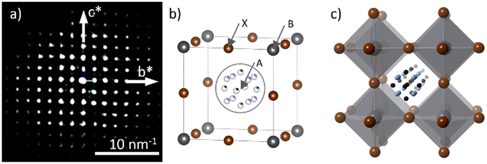 | ||
| Fig. 1 (a) ED projection along [001] used for the structure solution. (b) Schematic model of the unit cell solved by 3D-EDT, where the FA molecule is located at the centre of the cube, A site. (Because of cubic symmetry average, organic atoms have <1 occupancy.) Pb is located at the origin, B site, and Br is located at the middle of the edges, X site. This forms the ABX3 structure. (c) Polyhedral model of FAPbBr3, where the octahedral units are formed by Br in the corners and Pb in the center shown in grey, with the FA cations in the cavities. Color code: Pb – grey, Br – brown, N – blue, C – black. | ||
After obtaining the crystallographic information by 3D-EDT, we explored the possibility of imaging FAPbBr3 by spherical aberration corrected (Cs-corrected) STEM imaging using an annular dark field (ADF) detector (Fig. 2a). The selected area electron diffraction (SAED) pattern (inset) allows the identification of the pristine FAPbBr3. This result is quite significant as it allows tilting the crystal into the desired zone axis with less beam damage. In the image, small nanoparticles (NPs) of about 4 nm can be already identified (red arrow). These particles could be formed during preliminary observation as they were already there since the first scan, but they did not exhibit crystallinity as corroborated by the Fourier diffractogram (FD; shown in the inset), where only the diffraction planes indexed as (100) and (010) and separated by 5.94 Å, associated with the cubic phase of FAPbBr3, were observed, in agreement with the reported cubic form of FAPbBr3 at room temperature21,25 and in concordance with the ED analysis. A similar observation of the NPs has been reported during sample insertion at room temperature for MAPbI3,19 associated with the exposition of MAPbI3 nanowires to moisture. Here, we cannot either discard that the e-beam used for the current case, 156 e− Å−2, may cause a mild beam damage that still, however, allows the visualization of the pristine FAPbBr3. A closer visualization (green square) is displayed in the inset; the strongest signal in the corners of the cubic cell is associated with the columns where Pb alternates with Br. In between, there is a weaker signal that belongs to columns only formed by Br and finally, in the central part of the cubic cell, a weaker “rounded” signal that belongs to the FA cation composed by C, N and H was also detected. The schematic model was overlaid showing a good agreement with the experimental image, where Pb is shown in grey, Br in brown and C and N in black and light blue, respectively (for the sake of clarity, H is omitted due to its low contribution to the experimental image). The simulated data was superimposed on the right bottom of the magnified data in the green square showing a good match between the structural model obtained by 3D-EDT and the high-resolution images.
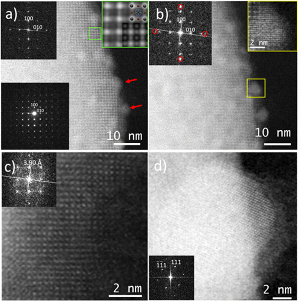 | ||
| Fig. 2 EM analysis of FAPbBr3. (a) Cs-corrected STEM-ADF image along [001] of the initial material; the ED pattern and FD are shown in the bottom and top left corner insets, which can be indexed as Pmm. Red arrows indicate small NPs which were present before imaging. The FAPbBr3 framework (green square) is magnified in the top right corner with the schematic model and simulated data overlaid. (b) Second scan showing the crystallization of Pb NPs (yellow square). Additional diffraction spots appear in the FD, indicated by red circles. (c) Further transformation of the FAPbBr3 structure into an intermediate where the Pb distance is significantly reduced. (d) Final image of the amorphized FAPbBr3 crystal with a Pb NP sitting on the [110] zone axis; the FD of the NP is shown in the inset. | ||
In the second scan, Fig. 2b, applying an electron dose of 310 e− Å−2, additional spots appeared in the FD (inset), associated with the crystallization of the NPs that were initially observed. A closer look at one of the NPs (yellow square) revealed the atomic distribution with the atomic columns separated by ≈2.4 Å, which was in agreement with the (200) of Pb. Interestingly, under this electron dose, besides the formation of crystalline Pb NPs, the FAPbBr3 unit cell suffered a contraction being a = 5.78 Å. In a subsequent scan, the FAPbBr3 suffered a deeper transformation (Fig. 2c), despite the symmetry of the crystal seemed to remain, the high resolution analysis and the FD (inset) showed that the distance between Pb atomic columns was significantly reduced to 3.90 Å. Fig. 2c presents the atomic-resolution micrograph of the partially damaged structure, which did not correspond to PbBr2, despite PbBr2 have been reported as the ultimate phase under electron beam irradiation.12 There are intermediate structures as a result of the organic and halide depletion.20,26,27 In the current situation, Fig. 2c is attributed to an intermediate phase prior to the full conversion into PbBr2. The FD in the inset does not show the {100} lattice planes observed for the pristine materials and the d-spacing measured in the new structure corresponded to the spots that were situated at ≈3.9 Å rather than at ≈5.94 Å, which would correspond to a value 1.5 times shorter than the distance from the initial Pb atomic columns and it is similar to the data reported20 for HA2(MA)n−1PbnI3n+1. Finally, the FAPbBr3 structure completely disappeared (Fig. 2d), leaving an amorphous material with the Pb NPs still present (in this case a Pb NP is shown along the [110] zone axis, as confirmed by the FD inset). Interestingly, under this condition no PbBr2 formation was observed. The EDS maps of the FAPbBr3 during electron illumination series were also collected. The result shows a shape transformation, organic element fading and also a slight increase in the Pb atom proportion (Fig. S5, ESI†).
A great advantage of EM over other characterization methods is that each particle can be fully characterized independently, which allowed the identification of a distinct phase.21
The unit cell parameters of the minor phase obtained from the 3D-EDT can be summarized as a = b = 8.4 Å, c = 14.5 Å and α = β = γ = 90°. The reflection condition was checked by the slice cut view of the reconstructed 3D reciprocal space from one of the datasets with 3904 reflections (510 unique reflections, completeness of 90.81% at 0.64 Å resolution), suggesting the I4/mcm space group (Fig. S6, ESI†). Table S3 (ESI†) shows the structure solution and refinement information. Fig. 3 shows the EDT slices along the three main crystallographic zone axes and the final structure solution along the 4-fold symmetry [001] direction. This structure is in agreement with an ammonium lead bromide reported in 1937.28 This space group, I4/mcm, has also been reported for MAPbBr3 at low temperature;29 however, there is no evidence for its existence at room temperature and for the case of FAPbBr3. Fig. S7 (ESI†) shows a view of the tetragonal structure along different orientations. It is worth noting that the weak electrostatic potential signal (Fig. S7d, ESI†) obtained was assigned to N; however, at this stage we cannot determine if that signal corresponds to N, C or both.
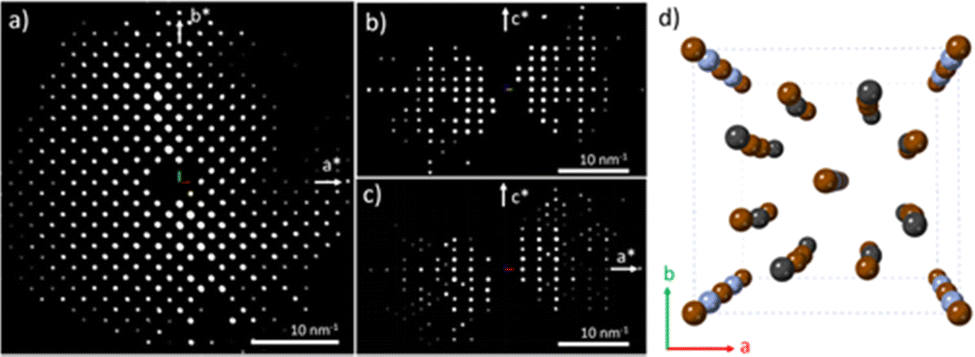 | ||
| Fig. 3 ED slices of the tetragonal minor phase extracted from the reconstructed 3D tomogram along three different zone axes: (a) [001], (b) [110] and (c) [010]. This tomogram shows a reflection condition of hkl = h + k + l; hk0 = h + k; 0kl = k,l; hhl = l; 00l = l; 0k0 = k, 4/mmm Laue class. (d) Structure results of 3D-EDT solution and refinement. Color code: Pb, grey; Br, brown; and N, blue. | ||
Fig. 4a presents the ED pattern along [001] in agreement with the data obtained by 3D-EDT, and the absence of extra spots corroborates the possibility of tilting the crystal without beam damage as no structural transformation took place. Fig. 4b depicts the Cs-corrected high-resolution STEM-ADF image, in the [001] direction, of the edge of a crystal, where the framework can be clearly observed. The surface of this particle contains already an amorphous phase probably owed to the sample preparation or due to contamination as the sample was exposed to the atmosphere. The FD, in the inset, is similar to the ED data recorded, which means that no structural transformation occurred under imaging. The atomic resolution data are shown in Fig. 4c with the structural model obtained from 3D-EDT superimposed. The simulated data is presented on the top right corner (yellow square). The tetragonal phase observed here was found to be more stable than the cubic one under e-beam irradiation, allowing the acquisition of several images of the same region under an electron dose of 500 e− Å−2.
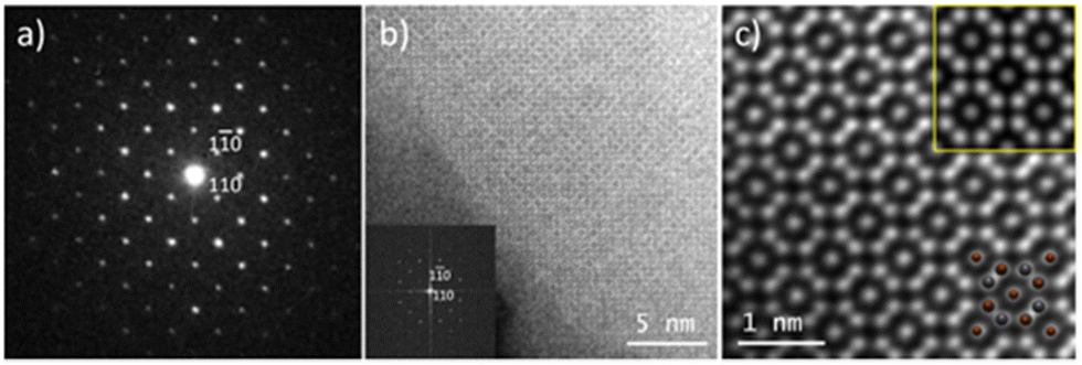 | ||
| Fig. 4 SAED pattern and Cs-corrected STEM-ADF image of the tetragonal minor phase taken along the [001]. (a) SAED pattern, (b) STEM-ADF with FD obtained from the image, (c) the magnified image where both the simulated image and the structure solution based on the 3D-EDT analyses (Pb in grey and Br in brown) are overlaid in the top right and bottom, respectively. | ||
Powder X-ray diffraction (PXRD) analysis was also used to investigate the crystal structures (Fig. S8 and S9, ESI†). The experimental PXRD data clearly indicate the existence of a highly crystalline cubic major phase. This was confirmed by Pawley refinement, resulting in a primitive cubic crystal lattice with a = 5.9928 Å. Considering that an additional minor phase was already solved by electron crystallography, we also simulated the PXRD pattern using the structure solution obtained, observing that some of the extra reflections not associated to the cubic one matched with this tetragonal phase. However, some other less intense peaks were observed which could indicate that the extra reflections would be due to background noise (probably a substrate effect). This observation highlights the benefits of TEM to study minor phases hardly detectable by XRD methods.
In summary, FAPbBr3 crystals have been investigated by different EM techniques to evaluate the possibility of analyzing this material at atomic resolution. 3D-EDT was used and the structure was, for the first time, solved by this method, opening up the possibility of obtaining crystallographic information when they are prepared in the nanoscale form. One of the advantages of EM is the possibility of treating individual particles as single crystals, which allows us to identify and solve a minor phase with tetragonal symmetry. Atomic-resolution imaging was performed on both structures (cubic and tetragonal) visualizing for the first time the structure of FAPbBr3 at the atomic level. In addition, the structural transformation that took place under e-beam irradiation has been also reported, displaying a shrinkage in the unit cell parameters most likely to be attributed to the loss of the organic and the halide. Finally, the tetragonal phase, which was solved by 3D-EDT, was also imaged at the atomic scale, resulting in a much more stable material under e-beam irradiation.
C. L.: data curation, investigation, writing – original draft; E. J. P.: investigation, resources; A. M.: conceptualization, investigation, project administration, supervision, writing – original draft, review & editing.
Funding support has been received from the MCIN (RYC2018-024561-I) and DGA (E13_20R), the European Union's Horizon 2020 research and innovation programme (823717 – ESTEEM3), the NFSC (21850410448 and 21835002) and The Centre for High-resolution Electron Microscopy (CħEM), ShanghaiTech University (EM 02161943). E. J. J.-P. acknowledges MCIN/AEI/10.13039/501100011033 and European Union Next Generation EU/PRTR (PID2019-107893RB-I00 and EIN2020-112315, respectively). The authors would like to thank Professor Osamu Terasaki for scientific discussion.
Conflicts of interest
The are no conflicts to declare.Notes and references
- A. Kojima, K. Teshima, Y. Shirai and T. Miyasaka, J. Am. Chem. Soc., 2009, 131, 6050–6051 CrossRef CAS PubMed.
- I. Suarez, E. J. Juarez-Perez, J. Bisquert, I. Mora-Serp and J. P. Martinez-Pastor, Adv. Mater., 2015, 27, 6157–6162 CrossRef CAS PubMed.
- M. R. Leyden, L. Meng, Y. Jiang, L. K. Ono, L. Qiu, E. J. Juarez-Perez, C. Qin, C. Adachi and Y. Qi, J. Phys. Chem. Lett., 2017, 8, 3193–3198 CrossRef CAS PubMed.
- M. Ahmadi, T. Wu and B. Hu, Adv. Mater., 2017, 29, 1605242 CrossRef PubMed.
- M. M. Lee, J. Teuscher, T. Miyasaka, T. N. Murakami and H. J. Snaith, Science, 2012, 338, 643–647 CrossRef CAS PubMed.
- Q. Jiang, Y. Zhao, X. Zhang, X. Yang, Y. Chen, Z. Chu, Q. Ye, X. Li, Z. Yin and J. You, Nat. Photonics, 2019, 13, 460–466 CrossRef CAS.
- Best NREL Research-Cell Efficiency Chart, https://www.nrel.gov/pv/cell-efficiency.html).
- L. K. Ono, E. J. Juarez-Perez and Y. Qi, ACS Appl. Mater. Interfaces, 2017, 9, 30197–30246 CrossRef CAS PubMed.
- I. Ciria-Ramos, N. Navascues, F. Diaw, C. Furgeaud, R. Arenal, A. Anson-Casaos, M. Haro and E. J. Juarez-Perez, Carbon, 2022, 196, 1035–1046 CrossRef CAS.
- S. Chen, X. Zhang, J. Zhao, Y. Zhang, G. Kong, Q. Li, N. Li, Y. Yu, N. Xu, J. Zhang, K. Liu, Q. Zhao, J. Cao, J. Feng, X. Li, J. Qi, D. Yu, J. Li and P. Gao, Nat. Commun., 2018, 9, 4807 CrossRef PubMed.
- D. Zhang, Y. Zhu, L. Liu, X. Ying, C. E. Hsiung, R. Sougrat, K. Li and Y. Han, Science, 2018, 359, 675–679 CrossRef CAS PubMed.
- M. U. Rothmann, J. S. Kim, J. Borchert, K. B. Lohmann, C. M. O’Leary, A. A. Sheader, L. Clark, H. J. Snaith, M. B. Johnston, P. D. Nellist and L. M. Herz, Science, 2020, 370, 6514 CrossRef PubMed.
- S. Chen and P. Gao, J. Appl. Phys., 2020, 128, 010901 CrossRef CAS.
- F. L. Deepak, A. Mayoral and R. Arenal, Advanced Transmission Electron Microscopy: Applications to Nanomaterials, Springer International Publishing, 2015 Search PubMed.
- A. Mayoral, M. Sanchez-Sanchez, A. Alfayate, J. Perez-Pariente and I. Diaz, ChemCatChem, 2015, 7, 3719–3724 CrossRef CAS.
- A. Mayoral, R. M. Hall, R. Jackowska and J. E. Readman, Angew. Chem., Int. Ed., 2016, 55, 16127–16131 CrossRef CAS PubMed.
- A. Mayoral, Y. Ma and O. Terasaki, Isr. J. Chem., 2018, 58, 1157–1163 CrossRef CAS.
- C. Li, Q. Zhang and A. Mayoral, ChemCatChem, 2020, 12, 1248–1269 CrossRef CAS.
- Y. Li, W. Zhou, Y. Li, W. Huang, Z. Zhang, G. Chen, H. Wang, G. H. Wu, N. Rolston, R. Vila, W. Chiu and Y. Cui, Joule, 2019, 3, 2854–2866 CrossRef CAS PubMed.
- K. Song, L. Liu, D. Zhang, M. P. Hautzinger, S. Jin and Y. Han, Adv. Energy Mater., 2020, 10, 1904006 CrossRef CAS.
- E. C. Schueller, G. Laurita, D. H. Fabini, C. C. Stoumpos, M. G. Kanatzidis and R. Seshadri, Inorg. Chem., 2018, 57, 695–701 CrossRef CAS PubMed.
- R. Chulia-Jordan and E. J. Juarez-Perez, J. Phys. Chem. C, 2022, 126, 3466–3474 CrossRef CAS PubMed.
- E. J. Juarez-Perez, L. K. Ono and Y. Qi, J. Mater. Chem. A, 2019, 7, 16912–16919 RSC.
- A. García-Fernández, E. J. Juarez-Perez, S. Castro-García, M. Sánchez-Andújar, L. K. Ono, Y. Jiang and Y. Qi, Small Methods, 2018, 2, 1800242 CrossRef.
- G. Laurita, D. H. Fabini, C. C. Stoumpos, M. G. Kanatzidis and R. Seshadri, Chem. Sci., 2017, 8, 5628–5635 RSC.
- A. R. Milosavljevic, W. Huang, S. Sadhu and S. Ptasinska, Angew. Chem., Int. Ed., 2016, 55, 10083–10087 CrossRef CAS PubMed.
- M. U. Rothmann, W. Li, Y. Zhu, A. Liu, Z. Ku, U. Bach, J. Etheridge and Y.-B. Cheng, Adv. Mater., 2018, 30, 1800629 CrossRef PubMed.
- H. Powell and H. Tasker, J. Chem. Soc., 1937, 119–123 RSC.
- M. Mączka and M. Ptak, Solids, 2022, 3, 111–121 CrossRef.
Footnote |
| † Electronic supplementary information (ESI) available: Details of synthesis, structure solution by 3D-EDT SEM and PXRD analysis. CCDC 2189650 and 2189651. For ESI and crystallographic data in CIF or other electronic format see DOI: https://doi.org/10.1039/d2cc04124c |
| This journal is © The Royal Society of Chemistry 2022 |