
 Open Access Article
 This Open Access Article is licensed under a Creative Commons Attribution-Non Commercial 3.0 Unported Licence
Two-photon polymerization lithography enabling the fabrication of PEDOT:PSS 3D structures for bioelectronic applications†
Amedeo
Ruggiero‡
 abc,
Valeria
Criscuolo
*a,
Sara
Grasselli
a,
Ugo
Bruno
ad,
Chiara
Ausilio
a,
Claudia Latte
Bovio
ad,
Ottavia
Bettucci
a and
Francesca
Santoro
*abc
abc,
Valeria
Criscuolo
*a,
Sara
Grasselli
a,
Ugo
Bruno
ad,
Chiara
Ausilio
a,
Claudia Latte
Bovio
ad,
Ottavia
Bettucci
a and
Francesca
Santoro
*abc
aTissue Electronics, Istituto Italiano di Tecnologia, 80125 Naples, Italy. E-mail: valeria.criscuolo@iit.it
bFaculty of Electrical Engineering and IT, RWTH Aachen, 52074, Germany
cInstitute for Biological Information Processing-Bioelectronics, Forschungszentrum Juelich, 52428, Germany. E-mail: f.santoro@fz-juelich.de
dDipartimento di Chimica, Materiali e Produzione Industriale, Università di Napoli Federico II, 80125 Naples, Italy
First published on 3rd August 2022
Abstract
Conductive 3D platforms have gained increasing attention in bioelectronics thanks to the improvement in the cell-chip coupling. PEDOT:PSS is nowadays widely employed in bioelectronic applications thanks to its electrical and mechanical properties. In this work, an innovative fabrication method for the realization of PEDOT:PSS-based conductive micropillars and 3D cage-like structures is presented, combining two-photon lithography and electrodeposition techniques.
Bioelectronic devices are electronic platforms that directly interact with biological systems, such as cells, tissues, or living systems, in order to monitor cellular electrical activity1 or modulate cellular behavior2 through the application of an external electrical field.3 Here, a crucial role is played by the interface between cells and electrodes that determines the effectiveness of the electrical coupling. In particular, the presence of a cleft between the membrane and the electrode represents a major limitation in the transduction of electrical signals.4 Several strategies have been developed to reduce the cleft at the interface, including the fabrication of protruding bioinspired microstructured electrodes featuring holes,5 grooves6 and pillars.7 The topography-mediated rearrangement of the cell membrane and cytoskeletal machinery, promoting the engulfment of the electrode, have been shown to improve the cell-chip coupling.8
Interestingly, organic conductive materials have been widely employed in bioelectronic devices thanks to their physical–chemical properties compared to inorganic materials, ranging from a higher versatility in synthesis and functionalization to fabrication and processability.9 Nowadays, poly(3,4-ethylenedioxythiophene) polystyrene sulfonate (PEDOT:PSS) is one of the most widely used conjugated polymers in several bioelectronic applications.10 It displays mechanical properties close to biological systems11 and shows a mixed ionic/electronic conduction mechanism,10 with hole conductivity above 1000 S cm−1,12 which is fundamental for an efficient cell-chip communication.13
Combining the beneficial effects of 3D microelectrodes in reducing the cleft and improving cellular adhesion with the properties of PEDOT:PSS can provide a step forward in the development of next generation bioelectronic and biomedical devices. Indeed, recently 3D PEDOT:PSS-based microstructures have been successfully developed by means of inkjet printing,14 3D printing,15 direct writing,16 replica molding17 and nanosphere lithography,18 and with the support of photocurable hydrogels.19 An interesting approach for the fabrication of 3D microelectrodes involves the fabrication of gold mushroom-like microstructures (with 1 μm in diameter) coated via electrodeposition of PEDOT:PSS precursors.20 However, as the 3D processing of PEDOT:PSS remains challenging, there is still a need to develop versatile patterning procedures that allow the integration of the material with microscale devices adapting to different geometries.
In recent years, two-photon polymerization (2PP) lithography has emerged as an effective method for the fabrication of 3D microstructures for numerous cell-material interfacing applications21 thanks to its high resolution (down to 100 nm)21 and design flexibility that enables the fabrication of complex 3D architectures without any geometrical constraint.22
In this work, we propose an innovative approach for the fabrication of conductive micropillars and 3D cage-like scaffolds exploiting 2PP and electrodeposition of PEDOT:PSS via cyclic voltammetry (CV). The proposed technique allows for the fabrication of PEDOT:PSS-coated micropillars as well as complex 3D structures that can fulfill any geometrical requirement, paving the way towards the development of 3D organic-based electrodes that can be tightly interfaced with biological systems and therefore can find a variety of applications in biosensing and cellular recording/stimulation.
The proposed fabrication process is schematically shown in Fig. 1A (see also Experimental section, ESI†). In this work, non-conductive micropillar arrays were fabricated by means of 2PP, employing the commercially available Ip-Dip negative photoresist: in particular, the micropillar diameter was 1 μm, while micropillars of different heights (from 1 μm to 5 μm) and pitches (from 1 μm to 10 μm) were fabricated. A layer of gold was then deposited via sputtering onto the micropillars and PEDOT:PSS was subsequently electrodeposited via a 3-electrode CV procedure (Fig. S1, ESI†).23 During the deposition process, the position of the working electrode (WE) can influence the film growth and assembly; here we first characterized PEDOT:PSS planar films obtained with a vertical and horizontal setting of the WE to determine the optimal conditions for the following functionalization of the micropillars (Fig. S2, ESI†).
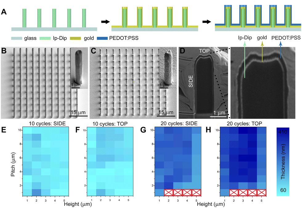 | ||
| Fig. 1 PEDOT:PSS micropillar array fabrication and thickness analysis. (A) Schematics of fabrication of micropillars via 2PP, coating with gold, and electrodeposition of PEDOT:PSS. (B) Scanning electron micrographs of a representative array (height 5 μm, pitch 4 μm) before and (C) after PEDOT:PSS electrodeposition. (D) Scanning electron micrograph of a PEDOT:PSS-coated micropillar cross-section. The thickness of the PEDOT:PSS film electrodeposited on different micropillar arrays is reported as a function of height and pitch: (E) 10 CV cycles measured on the side surface, (F) 10 CV cycles measured on the top surface, (G) 20 CV cycles measured on the side surface, and (H) 20 CV cycles measured on the top surface. | ||
By locating the WE above the electrolytic solution (Fig. S2E, ESI†), the electrodeposited PEDOT:PSS films displayed a uniform morphology (Fig. S2F, ESI†) and an average thickness of 72 ± 3 nm and 105 ± 5 nm when 10 and 20 CV iterations were performed, respectively (Fig. S3, ESI†). The latter configuration was then exploited to achieve a conformal PEDOT:PSS coating on micropillars arrays, preserving the initial geometry for both 10 and 20 applied CV deposition cycles (Fig. 1B and C, details in Fig. S4 and S5, ESI†). However, arrays with 1 μm pitch and micropillar heights from 2 to 5 μm showed a significant delamination from the substrate when 20 CV cycles were applied, probably due to an overgrowth of PEDOT:PSS that incorporates the arrays (Fig. S5, ESI†).
As the electrochemical properties of conjugated polymer films and electrodes strongly depend on their thickness and volume,24 the obtained 3D PEDOT:PSS micropillar geometry was further characterized by focused ion beam (FIB) cross sectioning and SEM imaging (Fig. 1D, Experimental section, ESI†). In particular, the film thickness was evaluated at the side and top surfaces of the micropillars and the resulting measurements are reported in Fig. 1E–H as a function of height and pitch. The micropillars obtained with 10 applied CV cycles exhibit an average thickness of ∼60 nm to ∼200 nm and the highest PEDOT:PSS thickness was found on the top of the micropillars in arrays with increasing pitch from 5 to 10 μm. The thickness was homogeneous on the micropillar side across arrays with a height from 4 to 5 μm and was higher in arrays with a height from 1 to 2 μm. In addition, micropillars obtained with 20 applied CV cycles displayed an average PEDOT:PSS film thickness ranging from ∼180 nm to ∼410 nm. In particular, the highest thickness (up to 410 nm) was found on the top surface of micropillars of height from 2 to 4 μm and pitch from 3 to 10 μm. Conversely, the film thickness on the side of the micropillars reached a maximum height of 330 nm. Interestingly, the overall PEDOT:PSS film thickness of the arrays with micropillars of 5 μm in height is lower, reaching a maximum of 290 nm. The overall higher PEDOT:PSS thickness observed on micropillar arrays (compared to the planar surface) can be ascribed to the larger electroactive surface area.25 In turn, the thickness difference found at the top and side of the micropillars may derive from the higher electric field induced by the tip effect.26
Then, the electrochemical impedance of the PEDOT:PSS-coated micropillars was investigated by means of EIS (Experimental section, ESI†). Bode plots measured for planar gold films (black trace) and PEDOT:PSS films electrodeposited with 10 and 20 applied CV cycles (red and blue trace, respectively) are reported in Fig. 2A and Fig. S6A (ESI†): here, at low frequencies a capacitive-dominated behavior emerges, as the modulus of the impedance decreases linearly with the frequency. In particular, the Bode modulus decreases faster when the capacitance of the substrate is higher. At higher frequencies, the modulus of the spectra is constant, suggesting a transition towards a more resistive-dominated behavior.27 It is worth noting that the PEDOT:PSS coating induces a shift of the capacitive-dominated behavior towards lower frequencies. In addition, larger shifts are induced by thicker polymeric layers (Fig. 2A, red and blue traces), due to the increase of the capacitance with the film thickness.27
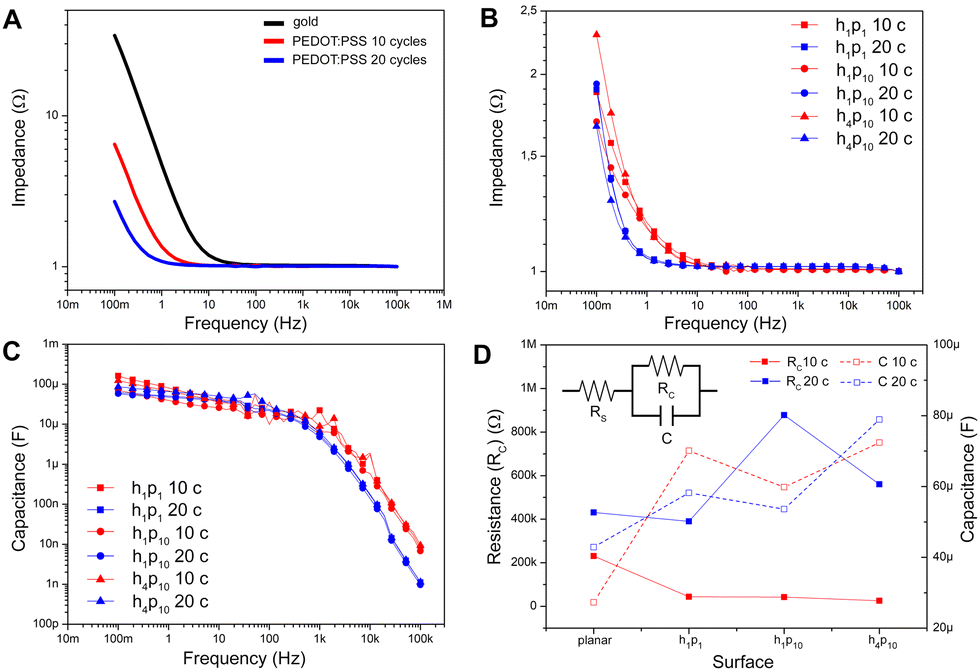 | ||
| Fig. 2 Electrochemical impedance spectroscopy characterization of PEDOT:PSS-coated pillar arrays. (A) Bode plots of planar gold film (black trace) and PEDOT:PSS films electrodeposited with 10 (red trace) and 20 (blue trace) CV cycles. (B) Bode plots of micropillar arrays coated with PEDOT:PSS films electrodeposited with 10 (red traces) and 20 (blue traces) CV cycles: h1p1 (squares); h1p10 (circles); h4p10 (triangles). (C) Capacitance plots of pillar arrays coated with gold PEDOT:PSS films electrodeposited with 10 (red traces) and 20 (blue traces) CV cycles: h1p1 (squares); h1p10 (circles); h4p10 (triangles). (D) Variation of the resistance Rc and capacitance C as a function of coated surfaces. The inset shows the equivalent circuit model used in this study. | ||
Furthermore, EIS measurements were performed on gold-coated and PEDOT:PSS-coated micropillar arrays of different height (1 and 4 μm) and pitch (1 and 10 μm) referred to as h1p1, h1p10, and h4p10. Representative impedance spectra are shown in Fig. 2B (more details in Fig. S6B, ESI†). Here, in contrast to the planar case, where the film thickness has also an effect on the impedance (Fig. 2A, red and blue traces), the Bode moduli corresponding to the micropillar arrays are similar regardless of the thickness of the polymeric film (Fig. 2B, red and blue traces), probably due to comparable values of capacitance as also shown in Fig. 2C.
Taken together, these findings suggest that the capacitance of microstructured electrodes is not linearly related to the thickness of the PEDOT:PSS film, whereas this linear relationship is maintained on planar substrates. In order to further confirm this hypothesis, EIS measurements were fitted with an electrical equivalent circuit shown in Fig. 2D (inset): here, the resistance RS models the electrolyte resistance and other parasite contributions, while the parallel between RC and C models the charge transfer resistance and the polymeric layer capacitance in PEDOT:PSS-coated micropillars.24 The ideal capacitance is replaced by a constant phase element (CPE) that includes the non-idealities of conducting polymeric thin films.28 Numerical data fitting extracted from planar electrodes (Table S1, ESI†) confirms that the equivalent PEDOT:PSS layer capacitance increases with the thickness.27 The dependency of RC and C on the shape of the micropillar arrays and PEDOT:PSS film thickness is shown in Fig. 2D (solid and dashed traces, respectively). In particular, PEDOT:PSS-coated micropillars are characterized by low values of resistance regardless of the height, density and number of CV applied cycles during the electrochemical deposition. Interestingly, the capacitance values of different micropillar arrays are comparable, showing no significant differences among electrodes with different PEDOT:PSS layer thickness, aspect ratios and spacings (h1p1, h1p10, h4p10). Moreover, the electrochemical properties of the electrodeposited PEDOT:PSS films were also assessed by means of CV acquired in the range between −1.0 to 1.0 V, using PBS as an electrolytic solution (Fig. S7, ESI†). The voltammograms showed the typical oxidation and reduction potentials of PEDOT:PSS, correlated to the PEDOT doped and de-doped state, and a reduction peak at + 0.6 V, in agreement with previous results.29
In conclusion, the electrochemical characterization supports the potential use of PEDOT:PSS-coated micropillars in bioelectronic devices for both in vitro sensing and stimulation. Indeed, the impedance is lower than 20 kΩ in the frequency range between 1 Hz and 5 kHz, which is usually considered the most relevant for extracellular neural electrophysiology.20 Moreover, the electrodeposited PEDOT:PSS films do not show redox activity in the ranges of potential typically employed for stimulation of electrogenic cells.10
Furthermore, in order to evaluate the biocompatibility of PEDOT:PSS-coated micropillars, a live/dead assay was performed after 1 day in vitro (DIV 1, Experimental section, ESI†) on both HT-22 cells (Fig. 3A, B and Fig. S8, ESI†) and primary cortical neurons (Fig. S9A and B, ESI†). Here, live and dead cells were labelled with Calcein-AM (green fluorescence signal) and a Dead Cell Stain Kit (blue fluorescence signal), respectively. In agreement with previous works,30 the PEDOT:PSS-coated micropillar arrays displayed high biocompatibility, with high percentages of live cells on both micropillars and flat regions (∼98%, Fig. 3C and Fig. S9C, ESI†). Scanning electron micrographs showed that PEDOT:PSS-coated micropillars promote cellular adhesion and elongation of neurites (Fig. 3D–F), which suggests that different aspect ratios of micropillars might support the cell-chip coupling and eventually act as topographical guidance. As the native cellular environment is elaborate and cells organize in a three-dimensional manner, preliminary studies were performed fabricating more complex conductive 3D cage-like scaffolds featuring microtowers, channels and micropillars with dimensions and topographical arrangement similar to previous works31 (details in the Experimental section and Fig. S10, ESI†). PEDOT:PSS was deposited applying 20 CV cycles to ensure a uniform and conformal coating. The scanning electron micrographs showed that, similar to what has been observed on micropillars, the PEDOT:PSS coating is conformal to the structure and the electrodeposition process did not affect the overall morphology of the designed structures (Fig. 4A). In addition, we investigated the thickness of the PEDOT:PSS film revealing the cross-section of the towers and the channels of the 3D cage-like structures via FIB cross sectioning (Fig. 4B and C). Interestingly, the overall PEDOT:PSS thickness reached a maximum of 160 nm, a value lower than the film thickness obtained on micropillar arrays (Fig. 4D). In particular, the towers featured with micropillars displayed a higher film thickness than the flat towers, with an average thickness of 134 ± 6 nm and 95 ± 9, nm respectively. Conversely, the PEDOT:PSS film thickness on the flat channels was higher than the thickness on channels with pillars, with an average thickness of 144 ± 8 nm and 127 ± 17 nm, respectively. In addition, the high standard deviation indicates the lower reproducibility of the PEDOT:PSS deposition on such narrow elements, compared to the other substrate regions (Fig. 4D). Furthermore, the biocompatibility of the PEDOT:PSS-coated 3D cage-like structures was assessed (details in the Experimental section, ESI†). As expected, cell survival was high both for HT-22 cells and primary cortical neurons (Fig. S11A and B, respectively, ESI†), which suggests that the spatial arrangement and morphology of the substrate have no effect on cell viability. Finally, cellular adhesion and interaction with the 3D structures was investigated via SEM imaging (Fig. 4E and F). The substrates support cellular adhesion, confining and guiding neurite outgrowth throughout the entire scaffold. Moreover, the presence of micropillars provides anchorage points for the elongation and growth of neuronal processes, allowing for a close cell-chip coupling, fundamental for an effective bioelectronic device.
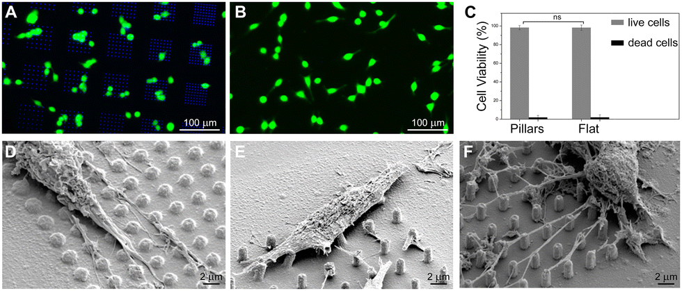 | ||
| Fig. 3 HT-22 cells cultured on PEDOT:PSS-coated micropillars. Fluorescence images of HT-22 cells showing live (green) and dead (blue) cells on (A) pillar arrays and (B) flat regions. (C) Percentage of live and dead cells reported as mean ± SD (n = 3). Scanning electron micrographs of HT22 cells on pillar arrays, coated with 10 applied CV cycles of PEDOT:PSS: (D) 1 μm high and 2 μm pitch, (E) 4 μm high and 6 μm pitch, and (F) 4 μm high and 3 μm pitch. | ||
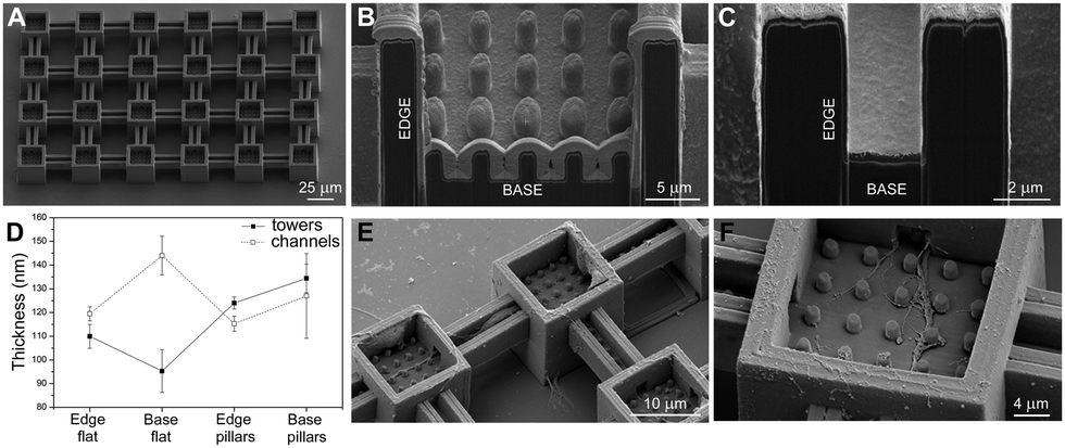 | ||
| Fig. 4 PEDOT:PSS-coated cage-like scaffold fabrication outcome, thickness analysis and cell-scaffold interaction. (A) Scanning electron micrograph of the 3D cage-like structures coated with 20 applied CV cycles. Scanning electron micrographs of cross-sections performed on different scaffold regions: (B) tower with pillars and (C) flat channel. (D) PEDOT:PSS thickness analysis on 3D structures: each graph shows the mean values and standard deviations depending on the cross-sectioned scaffold region. (E) Scanning electron micrograph of primary neurons cultured on 3D coated scaffolds and (F) close-up of a neurite wrapping around a pillar. | ||
In conclusion, in this work, an innovative and versatile fabrication method for 3D PEDOT:PSS-coated microstructures combining 2PP and electrodeposition techniques is reported. This method was employed for the fabrication of conductive micropillar arrays with various aspect ratios and pitches as well as complex 3D cage-like structures to demonstrate the versatility of the proposed technique. First, the resulting thickness of PEDOT:PSS according to the applied CV cycles on the micropillars was characterized by means of FIB cross-sectioning and SEM imaging. Subsequently, the electrochemical properties of the coated micropillars were investigated by means of EIS revealing that the presence of the 3D structures mediates the capacitance of the PEDOT:PSS film and is not dependent on the thickness. These findings demonstrate that the PEDOT:PSS-coated micropillars are suitable as electrodes to be implemented in bioelectronic devices for both sensing and stimulation of neuronal tissues. Additionally, we assessed the cell viability of HT22 cells confirming the biocompatible nature of PEDOT:PSS. Furthermore, it was observed that micropillar arrays can act as topographical guidance and that cage-like scaffolds were able to confine and guide neurite outgrowth. The results show that this fabrication method is suitable for the realization of conductive 3D structures of any kind of geometry, overcoming the limits of 2D cell cultures.
Francesca Santoro acknowledges the support of the European Research Council starting Grant BRAIN-ACT No. 949478. The authors acknowledge Dr Paschalis Gkoupidenis and Prof Roberto Centore for the scientific discussion corroborating the work.
Conflicts of interest
There are no conflicts to declare.References
- P. Mehrotra, J Oral Biol. Craniofacial Res., 2016, 6, 153–159 CrossRef PubMed.
- C. Chen, X. Bai, Y. Ding and I.-S. Lee, Biomater. Res., 2019, 23, 25 CrossRef PubMed.
- M. Rolandi, A. Noy, S. Inal and J. Rivnay, APL Mater., 2021, 9, 070402 CrossRef CAS.
- A. Zhang and C. M. Lieber, Chem. Rev., 2016, 116, 215–257 CrossRef CAS PubMed.
- T. J. J. Hondrich, B. Lenyk, P. Shokoohimehr, D. Kireev, V. Maybeck, D. Mayer and A. Offenhäusser, ACS Appl. Mater. Interfaces, 2019, 11, 46451–46461 CrossRef CAS PubMed.
- P. Wijdenes, H. Ali, R. Armstrong, W. Zaidi, C. Dalton and N. I. Syed, Sci. Rep., 2016, 6, 34553 CrossRef CAS PubMed.
- Micha E. Spira and Aviad Hai, Nat. Nanotechnol., 2013, 8, 83–94 CrossRef CAS PubMed.
- A. Mariano, C. Lubrano, U. Bruno, C. Ausilio, N. B. Dinger and F. Santoro, Chem. Rev., 2022, 122, 4552–4580 CrossRef CAS PubMed.
- D. Ohayon and S. Inal, Adv. Mater., 2020, 32, 2001439 CrossRef CAS PubMed.
- Y. Liang, A. Offenhäusser, S. Ingebrandt and D. Mayer, Adv. Healthcare Mater., 2021, 10, 2100061 CrossRef CAS PubMed.
- L. V. Kayser and D. J. Lipomi, Adv. Mater., 2019, 31, 1806133 CrossRef PubMed.
- J. Rivnay, S. Inal, B. A. Collins, M. Sessolo, E. Stavrinidou, X. Strakosas, C. Tassone, D. M. Delongchamp and G. G. Malliaras, Nat. Commun., 2016, 7, 11287 CrossRef PubMed.
- P. Zhang and J. Travas-Sejdic, J. Mater. Chem. C, 2021, 9, 9730–9760 RSC.
- I. Basak, G. Nowicki, B. Ruttens, D. Desta, J. Prooth, M. Jose, S. Nagels, H.-G. Boyen, J. D’Haen, M. Buntinx and W. Deferme, Polymers, 2020, 12, 2915 CrossRef CAS PubMed.
- H. Yuk, B. Lu, S. Lin, K. Qu, J. Xu, J. Luo and X. Zhao, Nat. Commun., 2020, 11, 1604 CrossRef CAS PubMed.
- P. Zhang, N. Aydemir, M. Alkaisi, D. E. Williams and J. Travas-Sejdic, ACS Appl. Mater. Interfaces, 2018, 10(14), 11888–11895 CrossRef CAS PubMed.
- Y.-S. Hsiao, B.-C. Ho, H.-X. Yan, C.-W. Kuo, D.-Y. Chueh, H. Yu and P. Chen, J. Mater. Chem. B, 2015, 3, 5103–5110 RSC.
- S. So, H. W. M. Fung, K. Kartub, A. M. Maley and R. M. Corn, J. Phys. Chem. Lett., 2017, 8, 576–579 CrossRef CAS PubMed.
- D. N. Heo, S.-J. Lee, R. Timsina, X. Qiu, N. J. Castro and L. G. Zhang, Mater. Sci. Eng., 2019, 99, 582–590 CrossRef CAS PubMed.
- P. D. Jones, A. Moskalyuk, C. Barthold, K. Gutöhrlein, G. Heusel, B. Schröppel, R. Samba and M. Giugliano, Front. Neurosci., 2020, 14, 405 CrossRef PubMed.
- C. Liao, A. Wuethrich and M. Trau, Appl. Mater. Today, 2020, 19, 100635 CrossRef.
- J. Harberts, C. Fendler, J. Teuber, M. Siegmund, A. Silva, N. Rieck, M. Wolpert, R. Zierold and R. H. Blick, ACS Nano, 2020, 14, 13091–13102 CrossRef CAS PubMed.
- X. Strakosas, B. Wei, D. C. Martin and R. M. Owens, J. Mater. Chem. B, 2016, 4, 4952–4968 RSC.
- G. Dijk, H. J. Ruigrok and R. P. O’Connor, Adv. Mater. Interfaces, 2020, 7, 2000675 CrossRef CAS.
- B. Rezaei, S. Saghir, J. Y. Pan, R. S. Davidsen and S. S. Keller, Micromachines, 2022, 13, 371 CrossRef PubMed.
- J. Wang, J. Zhang, X. Pei, S. Liu, F. Ning, Y. Li and C. Wang, CrystEngComm, 2020, 22, 2361–2370 RSC.
- D. A. Koutsouras, F. Torricelli, P. Gkoupidenis and P. W. M. Blom, Adv. Mater. Technol., 2021, 6, 2100732 CrossRef CAS.
- G. Inzelt and G. G. Láng, Electropolymerization, John Wiley & Sons, Ltd, 2010, pp. 51–76 Search PubMed.
- M. Marzocchi, I. Gualandi, M. Calienni, I. Zironi, E. Scavetta, G. Castellani and B. Fraboni, ACS Appl. Mater. Interfaces, 2015, 7, 17993–18003 CrossRef CAS PubMed.
- H. He, L. Zhang, X. Guan, H. Cheng, X. Liu, S. Yu, J. Wei and J. Ouyang, ACS Appl. Mater. Interfaces, 2019, 11, 26185–26193 CrossRef CAS PubMed.
- C. Fendler, C. Denker, J. Harberts, P. Bayat, R. Zierold, G. Loers, M. Münzenberg and R. H. Blick, Adv. Biosys., 2019, 3, 1800329 CrossRef PubMed.
Footnotes |
| † Electronic supplementary information (ESI) available: Experimental details and methods. See DOI: https://doi.org/10.1039/d2cc03152c |
| ‡ These authors contributed equally to this work. |
| This journal is © The Royal Society of Chemistry 2022 |