
 Open Access Article
 This Open Access Article is licensed under a
 Creative Commons Attribution 3.0 Unported Licence
A pyrrolopyridazinedione-based copolymer for fullerene-free organic solar cells†
Astrid-Caroline
Knall
 *ab,
Samuel
Rabensteiner
a,
Sebastian Franz
Hoefler
a,
Matiss
Reinfelds
a,
Mathias
Hobisch
c,
Heike M. A.
Ehmann
b,
Nadiia
Pastukhova
d,
Egon
Pavlica
d,
Gvido
Bratina
d,
Ilie
Hanzu
a,
Shuguang
Wen
e,
Renqiang
Yang
e,
Gregor
Trimmel
a and
Thomas
Rath
*a
*ab,
Samuel
Rabensteiner
a,
Sebastian Franz
Hoefler
a,
Matiss
Reinfelds
a,
Mathias
Hobisch
c,
Heike M. A.
Ehmann
b,
Nadiia
Pastukhova
d,
Egon
Pavlica
d,
Gvido
Bratina
d,
Ilie
Hanzu
a,
Shuguang
Wen
e,
Renqiang
Yang
e,
Gregor
Trimmel
a and
Thomas
Rath
*a
aInstitute for Chemistry and Technology of Materials (ICTM), NAWI Graz, Graz University of Technology, Stremayrgasse 9, 8010 Graz, Austria. E-mail: astrid.knall@anton-paar.com; thomas.rath@tugraz.at
bAnton Paar GmbH, Anton Paar Straße 20, 8054 Graz, Austria
cInstitute of Paper, Pulp and Fibre Technology, Graz University of Technology, Inffeldgasse 23, 8010 Graz, Austria
dLaboratory of Organic Matter Physics, University of Nova Gorica, Vipavska 11c, 5270 Ajdovščina, Slovenia
eCAS Key Laboratory of Bio-based Materials, Qingdao Institute of Bioenergy and Bioprocess Technology, Chinese Academy of Sciences, Qingdao 266101, China
First published on 24th December 2020
Abstract
The recent success of non-fullerene acceptors in organic photovoltaics also entails a change in the requirements to the polymer donor in terms of optical and morphological properties leading to a demand for novel conjugated polymers. Herein, we report on the synthesis of a 1,4-bis-(thiophene-2-yl)-pyrrolopyridazinedione based copolymer with 2-ethylhexyl substituents on the pyrrolopyridazinedione moiety. A 2D conjugated benzodithiophene (BDT) was chosen as comonomer. The resulting copolymer T-EHPPD-T-EHBDT showed a molecular weight of 10.2 kDa, an optical band gap of 1.79 eV, a hole mobility of 1.8 × 10⁻⁴ cm2 V−1 s−1 and a preferred face-on orientation with regard to the substrate. The comparably wide band gap as well as the determined energy levels (HOMO: −5.47 eV, LUMO: −3.68 eV) match well with the narrow band gap non-fullerene acceptor ITIC-F, which was used as the acceptor phase in the bulk heterojunction absorber layers in the investigated solar cells. The solar cells, prepared in inverted architecture, revealed power conversion efficiencies up to 7.4% using a donor:acceptor ratio of 1![[thin space (1/6-em)]](https://www.rsc.org/images/entities/char_2009.gif) :1 in the absorber layer.
:1 in the absorber layer.
Introduction
Non-fullerene acceptors (NFAs) have truly revolutionized organic photovoltaics by providing a step change in power conversion efficiencies (PCEs).1–3 Very recent studies have reported devices with PCEs up to 18%.4–7 Moreover, a simulation study revealed that efficiencies up to 20% can be achieved for single-junction devices and 25% for tandem solar cells.8 This requires balanced electron and hole mobilities together with low non-geminate recombination rate constants. These prerequisites, in addition to well-matched energy levels, drive the demand for novel materials, not only on the acceptor, but also on the donor side. In particular, wide bandgap materials have captivated researchers due to their complementary absorption properties to high-performance NFAs resulting in an improved utilization of the solar spectrum.9,10Tetrazine containing copolymers have recently gained interest as potential candidates to be combined with NFAs. Already some years ago, the strong electron-deficient character of tetrazines has motivated several groups to incorporate these monomers in conjugated copolymers, however, initially with moderate efficiencies for polymer:fullerene solar cells.11–16 Notably, the most efficient polymer:fullerene based devices emerged from polymers with 2D-conjugated benzodithiophene (BDT) as comonomer,17,18 a structural motif present in several highly efficient wide bandgap p-type polymers.10,19–22 In a very recent approach using NFAs, a PCE of 13% could be obtained with a tetrazine containing conjugated polymer (PSFTZ, 4,8-bis(5-((2-butyloctyl)thio)-4-fluorothiophen-2-yl)benzo[1,2-b:4,5-b′]dithiophene-alt-3,6-bis(4-octylthiophen-2-yl)-1,2,4,5-tetrazine) in combination with the NFA Y6.7 This already high performance could be even further pushed by adding Pt(Ph)2(DMSO)2 to reach 16.35%, which was claimed to be due to morphology improvements.
Therefore, these nitrogen-containing monomers hold a strong promise, also because they can be straightforwardly obtained from the corresponding nitriles, however, there are some drawbacks as well, which call for further research effort. The poor solubility of bis(aryl)tetrazines, such as the frequently used 3,6-bis(5-bromothiophen-2-yl)-1,2,4,5-tetrazine, requires comonomers with large solubilising alkyl chains to warrant adequate solubility and processability. Attaching suitable alkyl chains to the flanking aromatic rings of the tetrazine unit improves the overall polymer solubility and thus increases the chain length of the polymer. This allows for tuning the polymer properties, but at the cost of more synthetic effort for obtaining the required nitriles. Recently, we followed the approach of incorporating large branched alkyl side chains into the tetrazine based monomer and attempted to combine the necessity of the large alkyl chains with the benefit of an improved phase separation and domain purity in the absorber layer as exemplified by Liu et al.23,24 Combination of this tetrazine-quaterthiophene copolymer with the NFA ITIC-F (3,9-bis(2-methylene-(3-(1,1-dicyanomethylene)-6-fluoro-indanone))-5,5,11,11-tetrakis(4-hexylphenyl)-dithieno[2,3-d:2′,3′-d′]-s-indaceno[1,2-b:5,6-b′]dithiophene) led to an efficiency of 2.6%.24 A similar polymer with a fluorine-substituted quaterthiophene sequence gave 5.1% efficiency which could be further improved to 7.9% by replacing the quaterthiophene sequence with a suitably substituted sexithiophene.25 Nevertheless, tetrazine-containing polymers suffer from limited thermal stability, as demonstrated by us and others. Thermogravimetric analysis of the tetrazine-containing polymers revealed a decomposition step with an onset of 288 °C. The corresponding mass loss of 3% can be assigned to the loss of one equivalent of nitrogen per repeating unit.24 Li et al. reported a 90% yield for this reaction which was in line with our observation.12
Compared to tetrazines, pyrrolopyridazine (PPD) monomers have an increased electron-deficient character and are furthermore more thermally stable than the respective tetrazines.26 PPD monomers can be obtained from an inverse-electron demand Diels–Alder reaction (iEDDA)27 between maleimides and the corresponding tetrazines. First investigations of this new monomer class have been carried out towards an application in electrochromic materials.26 Polymers containing this monomer unit are hardly investigated in photovoltaic devices. In a previous study, we copolymerized a pyrrolopyridazinedione (PPD) with BDT (benzodithiophene) and evaluated its performance in polymer:fullerene bulk heterojunction solar cells.28 The solar cells with PC70BM as acceptor showed a high VOC of 0.9 V and a good fill factor of 0.66, but the PCE remained moderate (4.5%). The same polymer in combination with PC61BM as acceptor gave a PCE of 3.66%.29 Moreover, pyridazines are expected to have a much higher thermal stability compared to tetrazines, as they do not undergo a nitrogen elimination reaction. Therefore, it was also possible to successfully apply this polymer for the in situ synthesis of copper indium sulfide nanocrystals directly in the polymer films at temperatures up to 195 °C leading to polymer/nanocrystal absorber layers for hybrid solar cells. The corresponding devices exhibited PCEs of up to 2.5%.28,30 The limiting factor in these devices was the low short circuit current. One potential reason for this can be the bulky alkyl side chains (decyl-tetradecyl) on the PPD unit within this polymer. In a previous investigation by Duan et al., longer alkyl chains were found to lead to non-ideal bulk heterojunction morphology, deteriorated charge transport characteristics, significant bimolecular recombination and lower short circuit currents.31 Therefore, we synthesized a T-EHPPD-T-EHBDT copolymer using 2-ethylhexyl substituents on the pyrrolopyridazinedione moiety and in addition to a thorough characterisation in terms of optical, morphological and electronic properties, the conjugated polymer was applied in non-fullerene organic solar cells in combination with the NFA ITIC-F.
Experimental
Monomer and polymer synthesis
3,6-Bis(5-bromothiophen-2-yl)-1,2,4,5-tetrazine32 and N-(2-ethylhexyl)-maleimide33 were synthesised according to literature procedures. [4,8-Bis[5-(2-ethylhexyl)-thiophen-2-yl]benzo[1,2-b:4,5-b′]dithiophene-2,6-diyl]bis(trimethylstannane) (BDT monomer, purity: 97%) and all other chemicals were purchased from commercial sources (Sigma-Aldrich, Alfa Aesar) and used as received.1,4-Bis(5-bromothiophen-2-yl)-6-(2-ethylhexyl)-5H-pyrrolo[3,4-d]pyridazine-5,7(6H)-dione (T-EHPPD-T monomer)
3,6-Bis(5-bromothiophen-2-yl)-1,2,4,5-tetrazine (0.521 g, 1.29 mmol, 1 eq.) and 1-(2-ethylhexyl)-1H-pyrrole-2,5-dione (0.403 g, 1.93 mmol, 1.5 eq.) were dissolved in 10 mL of ortho-dichlorobenzene in a 50 mL Schlenk tube under inert atmosphere. This solution was heated to 160 °C for 10 h. After full conversion of the starting material, which had been detected by thin layer chromatography, the solution was added to 50 mL of cold methanol and the resulting precipitate was filtered off and purified by column chromatography (cyclohexane/chloroform volume ratio: 3/1). 0.305 g (0.522 mmol, 40%) of the title compound were obtained as a yellow powder. The 1H NMR spectrum of this monomer is shown in Fig. S1 (ESI†).1H NMR (300 MHz, CDCl3, ppm): δ 8.62 (d, 2H, J = 4.2 Hz), 7.19 (d, 2H, J = 4.2 Hz), 3.67 (d, 2H, J = 7.2 Hz), 1.92–1.76 (m, 1H), 1.42–1.25 (m, 8H), 0.96–0.90 (m, 6H).
13C NMR (75 MHz, CDCl3, ppm): δ 167.5, 148.1, 139.5, 134.1, 131.8, 122.3, 121.2, 43.2, 38.4, 30.7, 28.6, 24.0, 23.1, 14.2, 10.5.
MS (APCI): m/z = 581.9 [M + H, 2x79Br]+, 583.9 [M + H, 79Br + 81Br]+, 585.9 [M + H, 2x81Br]+.
IR νmax/cm−1 (ATR-FTIR): 3104 (ν(![[double bond, length as m-dash]](https://www.rsc.org/images/entities/char_e001.gif) CH)), 2959 (ν(C–H)alkyl), 2920 (ν(C–H)alkyl), 2850 (ν(C–H)alkyl), 1710 (ν(CO)imide), 1558 (ν(CC)PPD), 1420 (ν(CC)thiophene), 1395 (ν(CC)thiophene), 1354 (ν(CC)thiophene), 1229 (ν(CC)thiophene).
CH)), 2959 (ν(C–H)alkyl), 2920 (ν(C–H)alkyl), 2850 (ν(C–H)alkyl), 1710 (ν(CO)imide), 1558 (ν(CC)PPD), 1420 (ν(CC)thiophene), 1395 (ν(CC)thiophene), 1354 (ν(CC)thiophene), 1229 (ν(CC)thiophene).
Copolymerization towards T-EHPPD-T-EHBDT
[4,8-Bis[5-(2-ethylhexyl)-thiophen-2-yl]benzo[1,2-b:4,5-b′]dithiophene-2,6-diyl]bis(trimethylstannane) (212.40 mg, 0.2348 mmol), 1,4-bis(5-bromothiophen-2-yl)-6-(2-ethylhexyl)-5H-pyrrolo[3,4-d]pyridazine-5,7(6H)-dione (136.98 mg, 0.2348 mmol), tris(dibenzylideneacetone)dipalladium(0) (Pd2(dba)3, 6.82 mg, 7.44 × 10⁻³ mmol), tri(o-tolyl)phosphine ((o-tol)3P, 10.88 mg, 35.7 × 10⁻³ mmol), and 5 mL anhydrous, degassed chlorobenzene were placed inside a 10 mL glass tube. The tube was sealed and degassed with nitrogen for another 20 min. Then, the sealed tube was placed into a conventionally heated sealed tube reactor (Monowave 50, Anton Paar, Graz, Austria) and subjected to the following temperature program: ramp to 180 °C for 10 min, hold at 180 °C for 30 min.From the resulting dark purple solution, the crude product was recovered by precipitation into cold methanol. The precipitate was directly filtered into an extraction thimble followed by subsequent Soxhlet extractions with acetone, cyclohexane, and chloroform. The majority of the polymer was dissolved in the chloroform fraction which was concentrated to 2 mL and precipitated into methanol. This precipitation was repeated twice to obtain the purified polymer. Yield: 169.1 mg (0.169 mmol, 72%).
1H NMR (500 MHz, CDCl3, ppm): δ 8.77–7.99 (br m, 2H), 7.67–6.50 (br m, 8H), 4.03–3.39 (br m, 1H), 3.39–2.62 (br m, 2H), 2.45–0.18 (br m, 48H).
GPC (1,2,4-trichlorobenzene, 150 °C): Mn = 10200 g mol−1, Mw = 16900 g mol−1, ĐM =1.65.
IR νmax cm−1 (ATR-FTIR): 3117 (ν(CH)), 3068 (ν(CH)), 2958 (ν(C–H)alkyl), 2870 (ν(C–H)alkyl), 1767, 1710 (ν(CO)imide), 1557 (ν(CC)PPD), 1485 (ν(CC)thiophene), 1449 (ν(CC)thiophene), 1400 (ν(CC)thiophene), 1367 (ν(CC)thiophene), 1316 (ν(CC)thiophene), 1224 (ν(CC)thiophene).
Thin film and solar cell preparation
Pre-patterned ITO-coated glass substrates (Lumtec Luminescence Technology Corp., 15 × 15 mm, 15 Ω sq−1) were cleaned by sonication in 2-propanol (40–50 °C, 60 min) and oxygen plasma treatment (FEMTO, Diener Electronic, 3 min). ZnO thin films were prepared via a sol–gel reaction of a zinc oxide precursor solution consisting of zinc acetate dihydrate (0.5 g, 2.3 mmol) in 2-methoxyethanol (5 mL) using ethanolamine (150 mL, 2.5 mmol) as the stabilizer.34 The zinc oxide precursor solution was stirred overnight under ambient conditions for the hydrolysis reaction, followed by filtration through a 0.45 μm polytetrafluoroethylene (PTFE) syringe filter before spin coating (4000 rpm, 30 s). The ZnO films were annealed under ambient conditions (150 °C, 15 min) and layers with thickness between 30 and 40 nm were obtained. The polymer was dissolved in chlorobenzene (5 mg mL−1), blended with ITIC-F9 in donor:acceptor ratios of 1:1 and 1:1.5 by weight and spin coated onto the substrates, respectively. A molybdenum(VI) oxide anode interfacial layer (10 nm, deposition rate: 0.1 Å s−1) and a silver anode (100 nm, 1.0 Å s−1) were deposited by thermal evaporation under reduced pressure (ca. 10−5 mbar) through a shadow mask (9 mm2).
Characterization techniques
Absorption spectra were recorded on the UV-Vis spectrophotometer UV-1800 (Shimadzu) in the range of 380–900 nm. Surface profilometry measurements were performed on a DektakXT stylus profiling system (Bruker) equipped with a 12.5 μm-radius stylus tip in order to determine the layer thickness and surface roughness of thin film samples. Line scans were recorded over a length of 1000 μm, with a stylus force of 3 mg, and a resolution of 0.33 μm per pt. Layer thickness and surface roughness values were derived from surface profiles using the Vision 64 software (Bruker).
Cyclic voltammetry measurements were carried out on a SP-50 potentiostat/galvanostat (BioLogic) in acetonitrile using a three-electrode setup consisting of a platinum mesh counter electrode, a laboratory made Ag/Ag+ (0.01 M AgNO3 in acetonitrile) reference electrode36 with a Vycor glass frit and an indium tin oxide (ITO) coated glass substrate (15 × 15 mm, 15 Ω sq−1, Kintec) coated with a thin film of T-EHPPD-T-EHBDT as working electrode. The reference electrode was calibrated against a ferrocene/ferrocenium solution (Fc/Fc+) in deoxygenated and anhydrous acetonitrile using tetrabutylammonium hexafluorophosphate (Bu4NPF6, 0.1 M) as supporting electrolyte. The measurements were done in inert atmosphere (N2) at a scan rate of 50 mV s−1. The ionisation potential (IP) and the electron affinity (EEA) were calculated from the onset of the oxidation and the reduction potential (Eox, Ered) of the polymer considering the energy level of Fc/Fc+ to be −4.8 eV below the vacuum level via
 | (1) |
 | (2) |
2D-GIWAXS measurements of polymer thin films spin coated on silicon substrates were performed on an Anton Paar SAXSpoint 2.0 system equipped with a Dectris 2D EIGER R 1M hybrid photon counting detector with 75 μm2 pixel size and using Cu Kα radiation at 50 kV and 1 mA, which was point collimated using automated scatterless slits. The incidence angle was set to 0.12° and the exposure time was 10 × 120 s. A spin coated silver behenate film was used for the angular calibration.
Atomic force microscopy (AFM) measurements were performed on an Anton Paar Tosca™ 400 atomic force microscope in tapping mode using Al-coated cantilevers (ARROW-NCR, NanoWorld AG) with a resonance frequency of 285 kHz and a force constant of 42 N m−1. All measurements were acquired at room temperature under ambient conditions. All calculations and image processing were done with Tosca™ analysis software (V7.4.8341, Anton Paar).
For the determination of the charge carrier mobility, organic field-effect transistors with a bottom-contact bottom-gate configuration (IPMS, Fraunhofer Institute) were used consisting of n++-Si substrates with 230 nm of thermally grown SiO2 as the gate dielectric (15 nF capacitance Ci) and pre-patterned pairs of gold electrodes with interdigitated geometry as the source and drain. The channel length and width were 20 μm and 10 mm, respectively. T-EHPPD-T-EHBDT thin films were spin-coated from chlorobenzene (layer thicknesses: 60 nm). All solutions, samples and devices were prepared and measured in an N2-filled glovebox with H2O and O2 levels below 10 ppm to avoid oxidative doping of the materials and ensure reproducibility of the experiments. The device characteristics were measured by contacting the source, drain and gate electrodes and applying different voltages to obtain transconductance (IDS–VGS) graphs. All measurements were performed using a Keithley 2400 source meter and a Keithley 6487 picoammeter. Each IDS–VGS graph (transfer curve) was constructed by sweeping the gate voltage from +40 V to −40 V and back to +40 V, with one measurement every 2 V. The drain voltage was either −5 V (linear regime) or −40 V (saturation regime). Transfer curves were used to extract the value of the ION/IOFF ratio by dividing the value of the observed current in the saturation regime when the transistor is on (VGS = −40 V) by the value of the current when the transistor is off (VGS = +20 V). Experimental data were analyzed using the standard field-effect transistor model.
Results and discussion
1,4-Bis(5-bromothiophen-2-yl)-6-(2-ethylhexyl)-5H-pyrrolo[3,4-d]pyridazine-5,7(6H)-dione (T-EHPPD-T) was prepared from 3,6-bis(5-bromothiophen-2-yl)-1,2,4,5-tetrazine (1) and N-(2-ethylhexyl)-maleimide (2), see Scheme 1. For the Diels–Alder reaction with inverse electron demand (iEDDA), elevated temperatures (160 °C) and long reaction times were needed due to the strong electron-deficient character of both the diene and the dienophile. Due to the limited thermal stability of the parent tetrazine, this reaction could be completed with only moderate yield of 40%. | ||
| Scheme 1 Synthesis of T-EHPPD-T. | ||
T-EHPPD-T was then converted into an alternating donor–acceptor copolymer using Stille cross-coupling polymerization with the 2D-conjugated BDT (4,8-bis(5-(2-ethylhexyl)-thiophen-2-yl)benzo[1,2-b:4,5-b′]dithiophene-2,6-diyl)bis(trimethylstannane) comonomer (Scheme 2).18 The resulting copolymer (T-EHPPD-T-EHBDT, 4,8-bis(5-(2-ethylhexyl)-thiophen-2-yl)benzo[1,2-b:4,5-b′]dithiophene-2,6-diyl]-alt-1,4-bis(thiophen-2-yl)-6-(2-ethylhexyl)-5H-pyrrolo[3,4-d]pyridazine-5,7(6H)-dione-5,5′-diyl), obtained in 72% yield, showed a molecular weight of 10.2 kDa, a narrow dispersity ĐM of 1.6, good solubility in chlorobenzene and good film forming properties (see also Table 1 and Fig. S2, ESI†). In the device fabrication, good wetting behaviour of the ZnO layers was observed and smooth films were formed as proven by AFM measurements (see Fig. 3C). The thermogravimetric analysis performed in helium atmosphere (see Fig. S3, ESI†) proves good thermal stability, with a decomposition temperature Td (5% mass loss) of 415 °C.
 | ||
| Scheme 2 Synthesis of T-EHPPD-T-EHBDT. | ||
| M n (kDa) | M w (kDa) | Dispersity ĐM | T d (°C) |
|---|---|---|---|
| 10.2 | 16.9 | 1.65 | 415 |
The UV-vis spectrum of a thin T-EHPPD-T-EHBDT film prepared via spin coating from a solution in chlorobenzene on a glass substrate is depicted in Fig. 1A and shows an absorption onset at 691 nm. This corresponds to a comparably wide optical band gap of 1.79 eV. Moreover, a weak shoulder at approx. 610 nm can be observed in the spectrum and the absorption maximum is situated at 549 nm. This makes T-EHPPD-T-EHBDT a good candidate for combination with narrow-bandgap NFAs since the most intense region of the solar spectrum can be efficiently absorbed by this polymer.9
 | ||
| Fig. 1 (A) UV-vis spectrum and (B) cyclic voltammetry data of T-EHPPD-T-EHBDT thin films (reference electrode: Ag/Ag+, solvent: acetonitrile). | ||
The positions of the energy levels were studied by cyclic voltammetry using an Ag/Ag+ reference electrode and Fc/Fc+ as a calibration standard. The cyclic voltammograms are shown in Fig. 1B. From the onset of the oxidation peak, an ionisation potential (EIP) of −5.47 eV was determined, which can be correlated to the HOMO of the polymer, if minor solvent effects are neglected. The electron affinity (EEA) obtained based on the onset of the reduction peak is −3.72 eV. This results in an electrochemical band gap of 1.75 eV, which is in accordance with the optical one. Using the optical band gap for the calculation of the LUMO energy level, a value of −3.68 eV is obtained. The respective values are summarized in Table 2.
The hole mobility of the synthesized polymer was investigated using organic field effect transistors (OFETs). Representative transfer characteristics of bottom-contact bottom-gate OFETs are shown in Fig. 2A. The hole mobilities (derived from four devices) and other OFET parameters were determined from the VGS sweep as explained in the experimental section and show an average hole mobility of 1.8 ± 0.1 × 10⁻⁴ cm2 V−1 s−1 (see Table 3), which is comparable to related conjugated polymers comprising BDT as a comonomer unit.17,38,39Table 3 summarizes also other OFET parameters including threshold voltage (VTH) and on/off ratio for increasing and decreasing VGS sweep. In Fig. 2B, we compare the measured transconductance (symbols) and the standard transistor model (dashed line), which was used to estimate the OFET parameters. The perfect match between the two curves comes from the fact that subthreshold conductivity is negligible. The subthreshold current is the IDS current for VGS values, which are higher than VTH. We note that VTH is negative and in addition it exhibits a negative shift after the VGS sweep. This indicates that the dielectric/polymer interface contains charging sites, which trap mobile carriers. In fact, substrate treatment and polymer deposition were not optimized in terms of OFET performances. Nevertheless, the transconductance exhibits relatively high on–off ratio and almost zero subthreshold current (Fig. 2B), which is ideal for electronic applications.
 | ||
| Fig. 2 (A) Typical transconductance characteristics (IDS–VGS) measured at a drain voltage of −40 V. (B) Comparison of typical transconductance characteristics with the standard transistor model (dashed line). | ||
2D-GIWAXS measurements revealed the molecular packing of the polymer in thin films (Fig. 3A and B). The GIWAXS pattern in Fig. 3A shows a lamellar diffraction peak at q = 3 nm−1 (corresponding to an interlamellar distance of 2.1 nm) in the in-plane direction which has a circular extension towards the out-of-plane direction. This indicates that the polymer film is not highly oriented and face-on and edge-on orientations coexist. However, the higher intensity of this diffraction feature in the in-plane direction suggests a slightly preferred face-on orientation with respect to the substrate. The broad ring-like feature at q = 16.5 nm−1 corresponds to a d-spacing of 0.39 nm, which is indicative of π–π stacking. Furthermore, the feature is more pronounced in the out-of-plane direction, which also indicates a slightly preferred face-on orientation of the polymer chains.
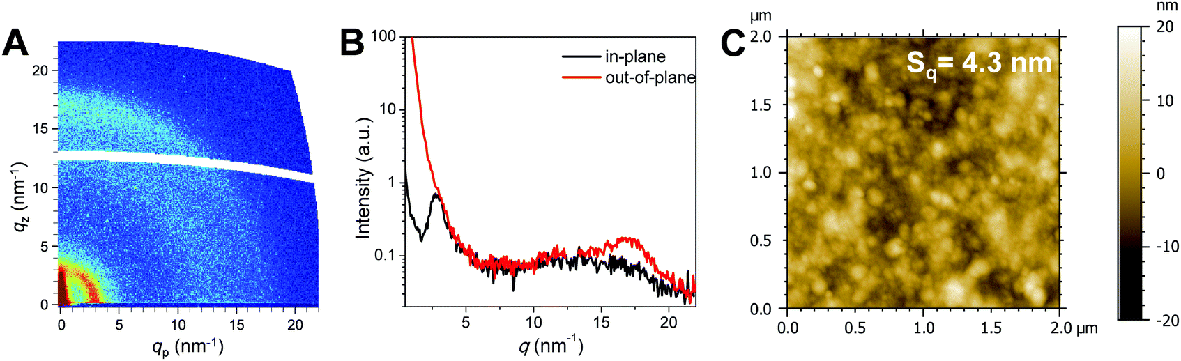 | ||
| Fig. 3 (A) 2D-GIWAXS pattern, (B) 1D-line cuts in the in-plane and out-of-plane directions and (C) AFM topography image of a T-EHPPD-T-EHBDT thin film. | ||
The AFM image shown in Fig. 3C reveals that the polymer films are very smooth and homogeneous with a surface roughness (Sq) of 4.3 nm.
For studying the performance of the polymer in non-fullerene organic solar cells, we aimed for a low band gap NFA with complementary absorption. NFAs like O-IDTBR,40,41 Y6,7,42 or ITIC and its fluorinated derivatives9,43,44 were found to fulfil this criterion. In addition, the matching of the energy levels with the synthesized copolymer (see Table 2) was considered which resulted in the selection of ITIC-F (HOMO: −5.69 eV, LUMO: −4.14 eV)9 as the acceptor component in the bulk heterojunction absorber layers. The corresponding energy level diagram is presented in Fig. 4A. In addition, as can be seen in Fig. S4 (ESI†), the absorption properties of these materials are complementary, which leads to a good coverage of the solar spectrum from 400 to 800 nm. Moreover, due to the similar hole mobility of T-EHPPD-T-EHBDT (1.8 × 10⁻⁴cm2 V−1 s−1) and electron mobility of ITIC-F (2.5 × 10⁻⁴cm2 V−1 s−1)43,45 a balanced charge transport in the bulk heterojunction can be expected.
 | ||
| Fig. 4 (A) Energy level diagram of the prepared T-EHPPD-T-EHBDT:ITIC-F solar cells and (B) the corresponding device architecture. | ||
The solar cells were prepared in an inverted device architecture using ZnO as electron transport and MoO3 as hole transport layer (see Fig. 4B). To optimize the photovoltaic performance of the T-EHPPD-T-EHBDT/ITIC-F solar cells, devices with absorber layer thicknesses from 50 to 140 nm were prepared with the two donor:acceptor weight ratios 1:1 and 1:1.5, respectively.
The AFM topography images of the blend films with T-EHPPD-T-EHBDT:ITIC-F weight ratios of 1:1 and 1:1.5 (Fig. 5A and B) reveal that the surface roughness is slightly increased for films with a higher acceptor content. The 1:1 film has a surface roughness (Sq) of 8.9 nm, for the 1:1.5 sample, this value is 9.6 nm. The corresponding phase images of these samples, depicted in Fig. 5C and D, reveal a very low phase contrast as expected due to the very similar chemical nature of the donor and acceptor phase in the blend films.
 | ||
| Fig. 5 (A and B) Topography and (C and D) phase AFM images of T-EHPPD-T-EHBDT:ITIC-F blend films with weight ratios of 1:1 and 1:1.5, respectively. | ||
The performance of the solar cells is significantly influenced by the absorber layer thickness as shown in Table S1 (ESI†). The highest PCEs were obtained with absorber layers with a thickness of 60 nm for both donor:acceptor ratios. With increasing thickness, mainly the FF is dropping, which can be ascribed to the comparably low charge carrier mobilities of both the donor and the acceptor leading to severer bimolecular recombination of charge carriers before they reach the respective electrodes.
The J–V curves (dark and illuminated) of the devices with 60 nm absorber layer thickness are depicted in Fig. 6A, the characteristic device parameters are summarized in Table 4. The highest PCEs of up to 7.4% were obtained with solar cells with a donor:acceptor ratio of 1:1. The J–V curves of this solar cell were additionally measured with a shadow mask, which leads to a reduction of the JSC of approx. 12% due to the elimination of the collection of charge carriers generated slightly outside the active area defined by the area of the Ag electrode, while the photovoltage and the fill factor stay constant, resulting in a PCE of 6.7%. On average (best 4–6 devices), these solar cells showed VOC values between 770 and 780 mV, photocurrent densities of 16.1 mA cm−2, fill factors of 0.58 and PCEs of 7.2%. As it is disclosed by the EQE spectra in Fig. 6B, the photocurrent generation is based on a contribution of both donor and acceptor. The EQE spectrum of the solar cell with the donor:acceptor ratio of 1:1 shows efficient current generation between 430 and 730 nm, whereby the current generation above 650 nm is mainly contributed by the acceptor ITIC-F. This is also reflected in the comparison of this solar cell with the one with higher amount of ITIC-F (1:1.5). Here, the higher amount of ITIC-F leads to an increased current generation in this wavelength range, while the photoresponse in the wavelength range of the polymer absorption is slightly reduced due to the comparably lower amount of T-EHPPD-T-EHBDT in the absorber layer blend. The highest PCEs obtained with the 1:1.5 blends were around 6.0%. Moreover, light intensity-dependent measurements of the JSC were performed and fitting of the data to the power law JSC ∝ Pαin (Pin: light intensity) led to values of the exponent α of 0.94 for the 1:1 ratio and 0.85 for the 1:1.5 ratio, see Fig. S5 (ESI†). This indicates a build-up of space charge in the solar cells prepared with the 1:1.5 ratio due to the higher ITIC-F content,46 which originates most presumably from a too high acceptor content negatively influencing a balanced charge carrier transport. This is also reflected in a significantly reduced FF as well as a slightly lower photovoltage of the solar cells prepared with a weight ratio of 1:1.5.
 | ||
| Fig. 6 (A) J–V characteristics of the solar cells with the highest PCE prepared with a T-EHPPD-T-EHBDT:ITIC-F weight ratio of 1:1 and 1:1.5 measured in the dark and under 100 mW cm−2 illumination and (B) the EQE spectra of these devices. | ||
| D:A ratio |
V OC (V) | J SC (mA cm−2) | FF | PCE (%) | R S (Ω cm2) | R SH (Ω cm2) | |
|---|---|---|---|---|---|---|---|
| a The average values and standard deviations are calculated from the best four devices. b The values in parenthesis represent data measured with a shadow mask (0.07 cm2). c R S and RSH values are determined as the inverse of the slope of the respective linear fit of the illuminated J–V curve at open circuit or short circuit conditions, respectively. | |||||||
| 1:1 |
Averagea | 0.778 ± 0.009 | 16.1 ± 0.8 | 0.58 ± 0.03 | 7.21 ± 0.12 | – | – |
| Best cellb | 0.773 (0.773) | 17.2 (15.1) | 0.56 (0.56) | 7.39 (6.71) | 7.1 | 459 | |
| 1:1.5 |
Averagea | 0.739 ± 0.009 | 15.1 ± 0.6 | 0.49 ± 0.01 | 5.52 ± 0.37 | – | – |
| Best cell | 0.754 | 15.6 | 0.50 | 5.96 | 8.6 | 460 | |
Moreover, the space-charge-limited current (SCLC) mobility of the blends was determined, as described in the ESI,† to be in the order of 10−5 cm2 V−1 s−1. Compared to the OFET hole mobility of the pure polymer, the SCLC mobility of the blend layers is approximately an order of magnitude lower, which is an expected result due to structural disorder introduced by the acceptor molecules.
Conclusion
The selected synthesis route towards the conjugated polymer T-EHPPD-T-EHBDT led to a polymer with a molecular weight of 10.2 kDa and a dispersity of 1.65. The synthesized polymer has an optical band gap of 1.79 eV and GIWAXS measurements disclosed a face-on orientation with regard to the substrate. The electronic properties were investigated via OFET-devices to obtain the hole mobility (1.8 × 10⁻⁴ cm2 V−1 s−1) and cyclic voltammetry to determine the energy levels (HOMO: −5.47 eV, LUMO: −3.68 eV). AFM measurements revealed the formation of smooth films with low surface roughness by the chosen spin coating conditions. The photovoltaic performance of the polymer T-EHPPD-T-EHBDT was evaluated in bulk heterojunction organic solar cells in inverted architecture. ITIC-F was selected as NFA due to its well matching optical and electronic properties. Using a donor:acceptor weight ratio of 1:1, PCEs of up to 7.4% were obtained and typical devices with this setup showed photovoltages between 770 and 780 mV, photocurrent densities of 16.1 mA cm−2 and fill factors around 0.58. External quantum efficiency spectra evidence the contribution of the conjugated polymer and the NFA to the photocurrent generation. Using donor:acceptor weight ratios of 1:1.5 in the absorber layer led to lower PCEs up to 6%. This is mainly due to the fact that the significantly higher amount of ITIC-F results in unbalanced charge transport and a build-up of space charge in the devices. Generally, the highest device performances were obtained with absorber layer thicknesses of 60 nm and even though only short solubilizing alkyl side chains have been applied, the polymer shows good solubility and processability.
Conflicts of interest
There are no conflicts of interest to declare.Acknowledgements
The authors thank Josefine Hobisch and Petra Kaschnitz for experimental support. A.-C. K. gratefully acknowledges financial support from the Austrian Science Fund (FWF) via Grant T578-N19. Furthermore, financial support by the OEAD S&T Cooperation program (project number CN 01/2016), the Ministry of Science and Technology of China (2016YFE0115000), the Austrian “Climate and Energy Fund” within the program Energy Emission Austria (project: Solabat, FFG No. 853 627), the Slovenian Research Agency (research core funding no. P1-0055) and the project RETINA, which is implemented and co-financed from the European Union – European Regional Development Fund in the frame of the Cooperation Programme Interreg V-A Slovenia-Austria in the programme period 2014-2020, is acknowledged.References
- A. Wadsworth, M. Moser, A. Marks, M. S. Little, N. Gasparini, C. J. Brabec, D. Baran and I. McCulloch, Chem. Soc. Rev., 2019, 48, 1596–1625 RSC.
- R. S. Gurney, D. G. Lidzey and T. Wang, Rep. Prog. Phys., 2019, 82, 036601 CrossRef CAS.
- P. Cheng, G. Li, X. Zhan and Y. Yang, Nat. Photonics, 2018, 12, 131–142 CrossRef CAS.
- M. A. Green, E. D. Dunlop, J. Hohl-Ebinger, M. Yoshita, N. Kopidakis and A. W. Y. Ho-Baillie, Prog. Photovolt. Res. Appl., 2020, 28, 3–15 CrossRef.
- Q. Liu, Y. Jiang, K. Jin, J. Qin, J. Xu, W. Li, J. Xiong, J. Liu, Z. Xiao, K. Sun, S. Yang, X. Zhang and L. Ding, Sci. Bull., 2020, 65, 272–275 CrossRef CAS.
- Y. Cui, H. Yao, J. Zhang, T. Zhang, Y. Wang, L. Hong, K. Xian, B. Xu, S. Zhang, J. Peng, Z. Wei, F. Gao and J. Hou, Nat. Commun., 2019, 10, 2515 CrossRef.
- X. Xu, K. Feng, Z. Bi, W. Ma, G. Zhang and Q. Peng, Adv. Mater., 2019, 31, 1901872 CrossRef.
- Y. Firdaus, V. M. Le Corre, J. I. Khan, Z. Kan, F. Laquai, P. M. Beaujuge and T. D. Anthopoulos, Adv. Sci., 2019, 6, 1802028 CrossRef.
- S. Wen, Y. Li, T. Rath, Y. Li, Y. Wu, X. Bao, L. Han, H. Ehmann, G. Trimmel, Y. Zhang and R. Yang, Chem. Mater., 2019, 31, 919–926 CrossRef CAS.
- H. Fu, Z. Wang and Y. Sun, Angew. Chem., Int. Ed., 2019, 58, 4442–4453 CrossRef CAS.
- Z. Li, J. Ding, N. Song, X. Du, J. Zhou, J. Lu and Y. Tao, Chem. Mater., 2011, 23, 1977–1984 CrossRef CAS.
- Z. Li and J. Ding, Macromol. Chem. Phys., 2011, 212, 2260–2267 CrossRef CAS.
- Z. Li, J. Ding, N. Song, J. Lu and Y. Tao, J. Am. Chem. Soc., 2010, 132, 13160–13161 CrossRef CAS.
- M.-J. Baek, W. Jang, S.-H. Lee and Y.-S. Lee, Synth. Met., 2012, 161, 2785–2791 CrossRef.
- J. Ding, N. Song and Z. Li, Chem. Commun., 2010, 46, 8668–8670 RSC.
- W. Cheng, Z. Wu, S. Wen, B. Xu, H. Li, F. Zhu and W. Tian, Org. Electron., 2013, 14, 2124–2131 CrossRef CAS.
- X. Guo, M. Zhang, L. Huo, F. Xu, Y. Wu and J. Hou, J. Mater. Chem., 2012, 22, 21024–21031 RSC.
- L. Ye, S. Zhang, L. Huo, M. Zhang and J. Hou, Acc. Chem. Res., 2014, 47, 1595–1603 CrossRef CAS.
- P. Zhu, B. Fan, L. Ying, F. Huang and Y. Cao, Chem. Asian J., 2019, 14, 3109–3118 CrossRef CAS.
- Y. Ma, Z. Kang and Q. Zheng, J. Mater. Chem. A, 2017, 5, 1860–1872 RSC.
- C. Gao, L. Wang, X. Li and H. Wang, Polym. Chem., 2014, 5, 5200–5210 RSC.
- Q. Wang, M. Li, Y. Sui, Z. Wang, Z. Liang and Y. Geng, J. Mater. Chem. C, 2019, 7, 9581–9590 RSC.
- Y. Liu, J. Zhao, Z. Li, C. Mu, W. Ma, H. Hu, K. Jiang, H. Lin, H. Ade and H. Yan, Nat. Commun., 2014, 5, 5293 CrossRef CAS.
- A.-C. Knall, S. F. Hoefler, M. Hollauf, F. Thaler, S. Noesberger, I. Hanzu, H. Ehmann, M. Hobisch, S. Spirk, S. Wen, R. Yang, T. Rath and G. Trimmel, J. Mater. Sci., 2019, 54, 10065–10076 CrossRef CAS.
- L. Peng, Y. Yu, J. Lu, P. He, G. Wang, M. Huang, B. Zhao, Y. Pei and S. Tan, Dyes Pigm., 2019, 171, 107717 CrossRef CAS.
- Q. Ye, W. T. Neo, C. M. Cho, S. W. Yang, T. Lin, H. Zhou, H. Yan, X. Lu, C. Chi and J. Xu, Org. Lett., 2014, 16, 6386–6389 CrossRef CAS.
- A.-C. Knall and C. Slugovc, Chem. Soc. Rev., 2013, 42, 5131–5142 RSC.
- A.-C. Knall, A. O. F. Jones, B. Kunert, R. Resel, D. Reishofer, P. W. Zach, M. Kirkus, I. McCulloch and T. Rath, Monatsh. Chem., 2017, 148, 855–862 CrossRef CAS.
- G. Zhang, J. Zhang, G. Ding, J. Guo, H. Lu, L. Qiu and W. Ma, Polymer, 2016, 93, 213–220 CrossRef CAS.
- T. Rath, D. Scheunemann, R. Canteri, H. Amenitsch, J. Handl, K. Wewerka, G. Kothleitner, S. Leimgruber, A.-C. Knall and S. A. Haque, J. Mater. Chem. C, 2019, 7, 943–952 RSC.
- C. Duan, R. E. M. Willems, J. J. van Franeker, B. J. Bruijnaers, M. M. Wienk and R. A. J. Janssen, J. Mater. Chem. A, 2016, 4, 1855–1866 RSC.
- D. K. Hwang, R. R. Dasari, M. Fenoll, V. Alain-Rizzo, A. Dindar, J. W. Shim, N. Deb, C. Fuentes-Hernandez, S. Barlow, D. G. Bucknall, P. Audebert, S. R. Marder and B. Kippelen, Adv. Mater., 2012, 24, 4445–4450 CrossRef CAS.
- J. Li, Y. Xiong, Q. Wu, S. Wang, X. Gao and H. Li, Eur. J. Org. Chem., 2012, 6136–6139 CrossRef CAS.
- Y. Sun, J. H. Seo, C. J. Takacs, J. Seifter and A. J. Heeger, Adv. Mater., 2011, 23, 1679–1683 CrossRef CAS.
- G. R. Fulmer, A. J. M. Miller, N. H. Sherden, H. E. Gottlieb, A. Nudelman, B. M. Stoltz, J. E. Bercaw and K. I. Goldberg, Organometallics, 2010, 29, 2176–2179 CrossRef CAS.
- G. Gritzner, Pure Appl. Chem., 1990, 62, 1839–1858 CAS.
- C. Liu, K. Wang, X. Hu, Y. Yang, C.-H. Hsu, W. Zhang, S. Xiao, X. Gong and Y. Cao, ACS Appl. Mater. Interfaces, 2013, 5, 12163–12167 CrossRef CAS.
- R. Duan, L. Ye, X. Guo, Y. Huang, P. Wang, S. Zhang, J. Zhang, L. Huo and J. Hou, Macromolecules, 2012, 45, 3032–3038 CrossRef CAS.
- L. Huo, S. Zhang, X. Guo, F. Xu, Y. Li and J. Hou, Angew. Chemie Int. Ed., 2011, 50, 9697–9702 CrossRef CAS.
- S. Holliday, R. S. Ashraf, A. Wadsworth, D. Baran, S. A. Yousaf, C. B. Nielsen, C.-H. Tan, S. D. Dimitrov, Z. Shang, N. Gasparini, M. Alamoudi, F. Laquai, C. J. Brabec, A. Salleo, J. R. Durrant and I. McCulloch, Nat. Commun., 2016, 7, 11585 CrossRef CAS.
- S. F. Hoefler, T. Rath, N. Pastukhova, E. Pavlica, D. Scheunemann, S. Wilken, B. Kunert, R. Resel, M. Hobisch, S. Xiao, G. Bratina and G. Trimmel, J. Mater. Chem. A, 2018, 6, 9506–9516 RSC.
- J. Yuan, Y. Zhang, L. Zhou, G. Zhang, H.-L. Yip, T.-K. Lau, X. Lu, C. Zhu, H. Peng, P. A. Johnson, M. Leclerc, Y. Cao, J. Ulanski, Y. Li and Y. Zou, Joule, 2019, 3, 1140–1151 CrossRef CAS.
- W. Zhao, S. Li, H. Yao, S. Zhang, Y. Zhang, B. Yang and J. Hou, J. Am. Chem. Soc., 2017, 139, 7148–7151 CrossRef CAS.
- N. Y. Doumon, F. V. Houard, J. Dong, H. Yao, G. Portale, J. Hou and L. J. A. Koster, Org. Electron., 2019, 69, 255–262 CrossRef CAS.
- Y. Lin, J. Wang, Z.-G. Zhang, H. Bai, Y. Li, D. Zhu and X. Zhan, Adv. Mater., 2015, 27, 1170–1174 CrossRef CAS.
- L. J. A. Koster, V. D. Mihailetchi, H. Xie and P. W. M. Blom, Appl. Phys. Lett., 2005, 87, 203502 CrossRef.
Footnote |
| † Electronic supplementary information (ESI) available: Additional characterization data and information about the determination of the SCLC charge carrier mobility. See DOI: 10.1039/d0nj04573j |
| This journal is © The Royal Society of Chemistry and the Centre National de la Recherche Scientifique 2021 |