
 Open Access Article
 This Open Access Article is licensed under a Creative Commons Attribution-Non Commercial 3.0 Unported Licence
2D material hybrid heterostructures: achievements and challenges towards high throughput fabrication
Laura
Maggini
 * and
Rúben R.
Ferreira
* and
Rúben R.
Ferreira
Institut für Organische Chemie, Universität Wien, 38 Währinger Strasse, A-1090 Wien, Austria. E-mail: laura.maggini@univie.ac.at
First published on 11th October 2021
Abstract
2D materials have attracted tremendous attention since the discovery of graphene, because of their unique optical/electronic/mechanical properties, and their manipulable bidimensional morphology. Since forthcoming technologies require a stringent yet faceted portfolio of features, hardly feasible using a single pristine material, the demand for property tuning and multifunctionality has led to the development of hybrid 2D material heterostructures to modulate and exploit the synergy between two or more materials and achieve novel properties. Because of their straightforwardness in implementation and rich variety of possible combinations, these hybrid architectures, held together mostly by non-covalent interactions, virtually allow the fabrication of any kind of assembly offering a unique opportunity for fine-tuning the properties of materials. However, reproducibility, scale-up, assembly into ordered structures and processability are the challenges yet to be addressed to technologically harness their full potential, and enable their integration into mass produced commercial devices. In this perspective article we analyse the recent developments in the automatised production of hybrid solution processed 2D material heterostructures, especially emphasising on the technologies that are currently closer to achieving low-cost, high-throughput standardised production, namely spray coating, inkjet printing and 3D printing, to sense the direction this research field is taking in pursuit of the development of commercialisable products.
 Laura Maggini | Laura Maggini obtained her master's degree in Chemistry at the University of Rome – Sapienza in 2006. She then joined the group of Prof. Bonifazi at the University of Namur as a PhD candidate, to pioneer the supramolecular functionalisation of CNTs with luminophores. Funded by two consecutive MSCA Individual Fellowships she then joined the group of Prof. De Cola at I.S.I.S., University of Strasbourg, to develop “breakable” hybrid silica NPs, and then that of Dr. De Volder at the Institute for Manufacturing (IfM), University of Cambridge, to study the functional assembly of nanomaterials exploiting manufacturing technologies. In 2020 she joined the University of Vienna as a Senior Researcher. Her research focuses on the development of high-throughput bottom-up production and manufacturing processes for hybrid organic materials, their processing and large area assembly for device integration. Her ambition is to develop innovative chemical methodologies to intimately engineer materials via a combined chemical and manufacturing approach, equally at the molecular, material (nano/micro-engineering) and architectural (macro-engineering) scales, to avoid deleterious interference and gain new tailorable properties/functions in the bulk. |
 Rúben R. Ferreira | Rúben R. Ferreira obtained his master's degree in Bioorganic Chemistry from the NOVA University of Lisbon in 2016. During his studies, Rúben worked in several projects with the Photochemistry and Supramolecular Chemistry Group. After completing his master's degree, Ruben joined the company Ynvisible – Lisbon, as a Researcher working on the development and characterization of electrochromic displays. During his work, Rúben worked in several European projects and collaborated with many companies, research institutes and universities. Later on, he assumed the position of Project Development Specialist and moved to Freiburg – Germany, where he helped set up the company's new R&D lab and managed internal and external development projects. In April of 2020, Rúben joined the group of Prof. Bonifazi at the University of Vienna as a PhD candidate, to develop new multi-functional electrochromic materials and devices based on covalent organic frameworks. |
1. Introduction
Since the discovery of graphene,1 the realm of 2D materials (2DMs) has flourished into a speckled range of chemical compositions including most elements of the periodic table, displaying a rich variety of unique mechanical and electronic properties:2–8 graphene, the most renowned, is a zero gap semiconducting,1 transparent, extremely strong (i.e., Young's modulus ∼1 TPa)9 yet flexible material;10 transition metal dichalcogenides (TMDs) are almost as thin, transparent and flexible as graphene (i.e., elastic moduli ∼a third of graphene),11 but as monolayers these are direct bandgap semiconductors (i.e., 1–2 eV; in the bulk their band gap is indirect);12,13 hexagonal boron nitride (h-BN) is a wide bandgap insulator (5.97 eV, optimal dielectric substrate),14–16 with high thermal and chemical stability, and thickness-independent mechanical strength comparable to graphene;17 black phosphorous (BP) is characterised by high mobility and thickness-dependent band gap18 (0.3–2 eV from bulk to monolayers);19 transition metal carbides and nitrides (MXenes) are mostly metallic (i.e., few systems expected to be semiconductors),20 with functionalization-dependent work functions (e.g., from 1.6 eV for Sc2C(OH)2 to 8.0 eV for Cr2CO2)21,22 and the highest effective Young's modulus upon indentation for solution-processed 2DMs (including graphene oxide).23 Additionally, the 2DM bidimensional geometry possesses excellent compatibility with currently exploited industrial manufacturing platforms, facilitating direct integration into industrial production processes (e.g., Si production line).24,252DMs have thus gained great thrust for implementation both in microscopic (e.g., (opto)electronics, photonic devices, sensing, energy storage, etc.) and macroscopic (e.g., composites, catalysis, water remediation, etc.) applications.26–28 However, forthcoming technologies based on advanced materials require a stringent yet faceted portfolio of properties (e.g., charge mobility, bandgap, optical transparency, flexibility, etc.), hardly feasible by a single 2DM. The example of graphene is compelling: despite its mechanical strength and flexibility, high charge carrier mobility, and optical transparency,29 the lack of a band gap in its electronic structure1 clearly prevented its effective implementation, for example, in (opto)electronic applications. To overcome the intrinsic limitations of individual 2DMs, physical and chemical methods to modulate their properties (e.g., structural, composition and external field tuning) have been promptly developed.30 Nonetheless, despite being effective, these approaches suffer severe reproducibility and scale-up issues, making them incompatible with the requirements for high-throughput product manufacturing.
With the aim of finding accessible, reproducible and non-destructive property-tuning methodologies, the paradigm shifted towards the hybridisation (i.e., vertical or lateral hierarchised stacking) of 2DMs with complementary materials of similar or other dimensionality (2D/0–1–2–3D)31 without chemical bonding, exclusively exploiting van der Waals interactions. This enabled the straightforward prototyping of a kaleidoscopic variety of heterostructures, macro-ordered architectures possessing bespoke composition-dependent physical and mechanical properties (Fig. 1).31,32
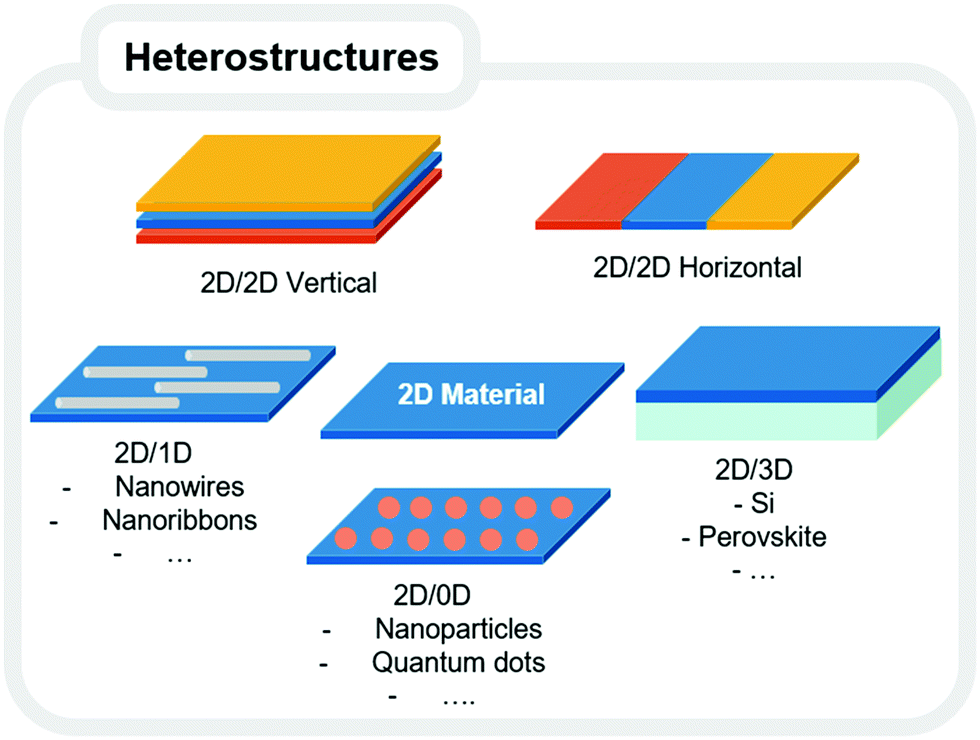 | ||
| Fig. 1 Schematic representation of the possible 2D material-based van der Waals heterostructures. Reproduced with permission.31 | ||
Specifically, by definition a heterostructure is a hybrid system presenting an interface between two materials.31,32 When these heterostructures are composed of two semiconductors with dissimilar band gaps, presenting a coupled interface in which these generate a band alignment or rectify a contact after the equilibration of the Fermi levels (or work functions), they are also defined as “heterojunctions”.33 These terms have often been used interchangeably and have sometimes generated confusion in the definition of more sophisticated bulk heterostructures (e.g., several heterojunctions, different dimensionality etc.) than the 2D/2D heterostructures composed of two atomic thin layers for which the terms heterostructure and heterojunction overlap. For the sake of clarity, we will only use the term heterostructure in this manuscript to address the reported hybrid architectures, independently of whether they also comply with the definition of the heterojunction.
The heterostructure approach, which could virtually lead to any desired combination, thus offers a unique synergistic opportunity to overcome the inherent limitations of each of its components and build tailored architectures at the limit of atomic resolution presenting improved or even unprecedented properties when compared to their constituting elements. The landmark production of graphene field effect transistors (FETs) supported by h-BN by Hone and coworkers in 201014 demonstrated that h-BN can serve as a perfect dielectric substrate effectively enabling graphene-based electronics, by reporting charge transport measurements up to 60![[thin space (1/6-em)]](https://www.rsc.org/images/entities/char_2009.gif) 000 cm2 V−1 s−1. Few years later the same group reported the production of FETs with a molybdenum disulfide (MoS2) channel, graphene gate and h-BN dielectric on flexible substrates,34 presenting mobility (27 cm2 V−1 s−1) comparable to that attainable on a rigid SiO2 substrate (45 cm2 V−1 s−1). Since then a profusion of heterostructures characterised by enhanced synergistic performance were produced, advancing their applicability in fields such as (opto)electronics, sensing, energy storage, catalysis, etc.30–32,35–41
000 cm2 V−1 s−1. Few years later the same group reported the production of FETs with a molybdenum disulfide (MoS2) channel, graphene gate and h-BN dielectric on flexible substrates,34 presenting mobility (27 cm2 V−1 s−1) comparable to that attainable on a rigid SiO2 substrate (45 cm2 V−1 s−1). Since then a profusion of heterostructures characterised by enhanced synergistic performance were produced, advancing their applicability in fields such as (opto)electronics, sensing, energy storage, catalysis, etc.30–32,35–41
The pioneering processes for the prototyping and fundamental investigations of 2DM heterostructures were the top-down mechanical exfoliation and the bottom-up chemical vapour deposition (CVD) techniques.30–32 Although producing the highest quality 2DMs, these technologies either lack scalability or remain costly and complex in their execution concerning heterostructure production.30–32 For instance, the exfoliation and restacking approach offers great design flexibility, but remains intrinsically not scalable in both size (i.e., μm range) and quantity of 2DM heterostructures produced.30–32 CVD, which requires high temperatures and high vacuum, is hindered by the sensitive growth conditions specific for each 2DM. Such restrictions hamper design flexibility and the growth of quality 2DMs onto prior layers without damage. Moreover, the mandatory requirement of a final transfer step from the growth substrate onto a target substrate might degrade the properties of the heterostructure either by damaging its structure (i.e., introducing defects, wrinkles, etc.), or by contaminating the hybrid's surface (i.e., residuals of polymeric carrier in wet transfer processes).32
To nonetheless harness the high quality of CVD produced 2DMs in heterostructures, researchers started to employ this process in combination with other manufacturing technologies (i.e., inkjet printing; vide infra Section 2.2), averting the growth condition incompatibility issue of different 2DMs. Quellmalz, Niklaus and coworkers recently reported a versatile approach for the transfer (i.e., monolayer graphene from copper foils to 10 cm Si wafers) and stacking of 2DMs into heterostructures (i.e., graphene/h-BN heterostructures; semiconducting double-layer graphene) by a resin-mediated “gluing” process (i.e., adhesive bonding), employing solely commercially available wafer bonding equipment.42 Specifically, a resin is initially spin coated onto the target substrate (2.5 μm), then the CVD grown monolayer of interest (i.e., on the Cu foil) is placed on top of the target wafer and bonded in a wafer bonder in an inert atmosphere (i.e., for graphene 190 °C, 20 min, 3 kN). Follow-up etching (i.e., FeCl3 to remove Cu foil) and rinsing steps provide the transferred material; to produce heterostructures the process is adapted (i.e., etching step depending on growth substrates) and repeated as many times as the required layers. The proposed methodology definitely represents a substantial advancement in the production of wafer size heterostructures through a process compatible with the high-volume production lines of the semiconductor industry. However, this process remains inherently elaborate, costly in its execution and limited in design flexibility (e.g., expensive masks for design; rigid substrates; etc.).
Accessible solution-processed heterostructures started to be produced via layer-by-layer assembly performed with nonautomated methodologies, such as drop casting, filtration, spin coating, etc.,43,44 exploiting single or few-layer 2DM suspensions obtained by ultrasonication and intercalation.45 Despite the straightforward implementation, the performance of these solution-processed heterostructures was negatively impacted by the lack of exact reproducibility, fine-tuning of their structural parameters (e.g., number of layers, thickness, roughness, etc.) and technical limitations (e.g., vacuum filtration: device-dependent size of the assembly, lengthy process, required transfer procedure, not scalable; spin coating: limited thickness to 50 nm, loss of homogeneity upon scaling up of the coated area, high wastage, not compatible with diluted solutions and flexible substrates) hindering scale up of production.45 Satisfactory and reliable performance among large scale productions is an essential requirement for the deployment of 2DMs in commercialisable products.24
The formulation of solution processable 2D materials into inks44,46–49 has eventually enabled the controlled (i.e., thickness, dimension, roughness, etc.) “functional” deposition (i.e., structure able to perform a function) of 2DMs, exploiting established printing and coating technologies. This transition towards automatised, low-cost and large-scale manufacturing technologies is foreseen capable of facilitating mass-market adoption of 2DMs,50 and is now starting to prove its disruptive advantages for the standardised fabrication of heterostructures, removing the need for developing new manufacturing technologies for these hybrids. Indeed, industrial-scale printing facilities have developed to satisfy the tight cost control of high volume manufacturing industries (e.g., packaging, newspapers, etc.) and are thus optimised for minimal operating costs (e.g., environmental temperature and pressure), swift mass-production (i.e., printing speeds >100 m min−1) and compatibility with flexible materials (i.e., paper, plastic, and textiles optimal for flexible and wearable electronics).50
Several reviews have been published on 2D material heterostructures26,30–32,38–41,51–61 focusing on material synthesis and characterisation of their chemical, physical, and optoelectronic properties. For state-of-the-art fabrication of 2D/3D heterostructures, we refer the readers to the critical survey by Kim et al. on the production of 2D materials onto bulk materials and vice versa.62 The scope of this perspective article is instead that of highlighting the recent advances in heterostructure fabrication exploiting industry-friendly solution-processing technologies (i.e., spray coating, inkjet printing and 3D printing) that are currently being explored for the preparation of heterostructures, paving the way to their automatised, reliable, large-scale production, hinting at their awaited integration in commercial products (Fig. 2).
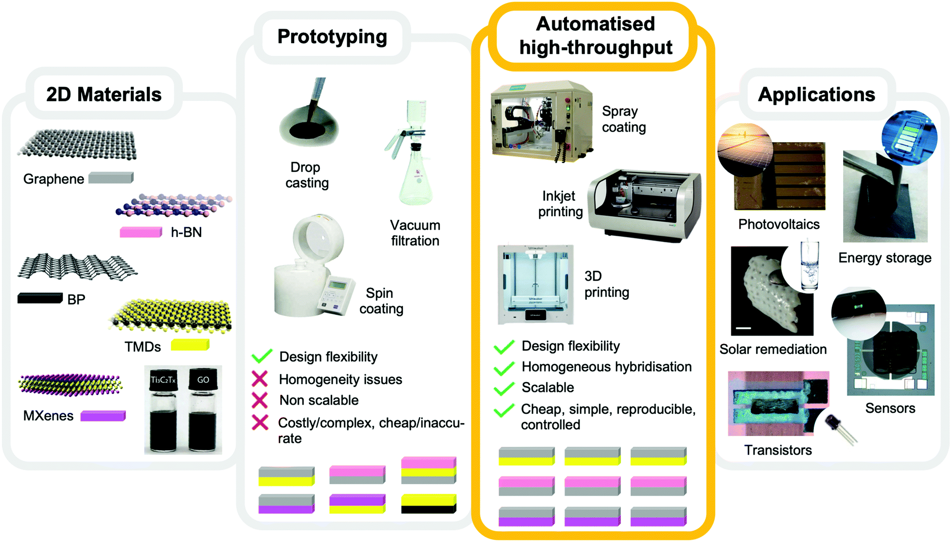 | ||
| Fig. 2 Schematic representation of the 2D material solution-processed heterostructure roadmap, from left to right: the exfoliation and solution processing of the 2DMs, the pioneering attempts of dry and wet heterostructure assembly which led to the fast prototyping of a kaleidoscopic variety of hybrid hierarchised architectures, the high throughput assembly processes reviewed in this Perspective Article today applied for their large scale standardised manufacturing leading to their integration into mass produced applications. Reproduced with permission.63–69 | ||
We herein review the latest scientific breakthroughs reported in the literature concerning the solution processed fabrication of 2DM heterostructures with coating and printing manufacturing technologies. Upon a thorough bibliographic research we specifically identified mainly three technologies currently thoroughly investigated for the achievement of the ambitious goal of optimising and standardising the manufacturing of 2D material heterostructure-based products, namely spray casting, inkjet printing and 3D printing. After a brief introduction on the machines, their technological improvements towards the delivery of bespoke heterostructures will be discussed as well as the specifics of the deposition strategy and device design/integration, providing a holistic overview on this research field from a combined engineering/manufacturing, materials science and chemical perspective. The examples reported have been selected not only for the performance improvement detected for the produced heterostructures, but most importantly on the merit of production homogeneity and performance reliability. Where possible, considering the limited amount of currently available literature for this cutting-edge research topic, the focus will be kept on the production of heterostructures tailored for integration into applications within the scope of this journal (e.g., transistors, photovoltaics, sensors, etc.).
2. Coating and printing technology-based heterostructure fabrication
The emergence of solution processed 2D materials and ink formulation43,44,46,48,49,70–72 has enabled their value-added harnessing into established coating and printing technologies, offering the promise of their automatised (i.e., consistent), scalable manufacturing and device integration (e.g., (opto)electronics, photonics, energy storage, sensing, etc.).44,73 Coating and printing technologies, including spray coating,74 inkjet printing,75 and extrusion-based 3D printing,76 have evolved to implement 2DM-based device manufacturing with high homogeneity and resolution, by adapting their printing components and processes to 2DM inks.46 In parallel, since the first example of inkjet-printed graphene-based flexible electronics reported in 2011,77 sustainable progress (e.g., shift to non-toxic, volatile solvents, conscious choice, use of additives and binders, etc.) in functional ink formulation enabled optimisation of the 2DM inks’ fluidic characteristics to match the printing requirements of the manufacturing platforms (e.g., viscosity, volatility, wettability, viscoelasticity, etc.) facilitating effective deposition, as well as improvement of the drying/adhesion (i.e., resolution) of the printed features.46In this section we will outline the recent achievements in the employment of these technologies for the large-area, high-volume production of functional 2D material heterostructures (e.g., both layer-by-layer and randomly assembled) and their implementation in the state-of-the-art devices characterised by property consistency advantages.
2.1 Spray coating
Spray coating is a versatile and cost-effective deposition technique suitable for the large-area coating of rigid and flexible substrates.78,79 A carrier gas (i.e., N2) pushes the liquid ink (viscosity: 1–1000 mPa s; 2D material loading: 0.1–10 w%) through a small nozzle towards the substrate.79 Once the droplets hit a surface they coalesce into a uniform wet film (resolution: 2–200 μm), which later solidifies upon evaporation of the solvent. Due to its divergent automatised spraying, a uniform and continuous film can be reproducibly achieved even in substrates with a highly rough surface. Furthermore, this technique allows fine tuning over film thickness and morphology by adjusting carrier gas pressure (size and speed of the droplets), the distance between the nozzle and the substrate, and substrate temperature.79In 2007 Kaner et al. demonstrated the potential of spray casting in the fabrication of highly uniform and semiconducting graphene sheets (i.e., with tailored size, thickness) obtained via the initial deposition of a graphene oxide aqueous dispersion followed by reduction.80 The combination of droplet size control and rapid evaporation (i.e., avoidance of the coffee ring effect and evaporation driven concentration), led to homogeneous reproducible films in nearly 100% yield within hours. This technology has only recently started to be exploited for the controlled production of 2D material heterostructures. In 2019 Gogotsi and coworkers reported the use of an airbrush for the scalable manufacturing of 2D MXene/graphene heterostructured free standing films by spray-assisted layer-by-layer assembly (Fig. 3).63 Specifically, by spraying alternating thin layers of Ti3C2Tx MXene and reduced graphene oxide (rGO), the authors obtained a hybrid flexible film with a thickness of 2–3 μm, combining the energy storage capability of MXenes with the electrical conductivity of graphene. Interestingly, the authors were able to produce 22 × 28 cm films within 30 min, indicating the possibility of high throughput fabrication. Moreover, when compared to their individual building blocks, the hybrid structure displayed improved electrochemical performance when used as an anode for Na-ion storage (4:1 ratio achieved a reversible capacity of 600 mA h g−1 at 0.25 °C > pristine Ti3C2Tx MXene 180 mA h g−1 and rGO films 45 mA h g−1).
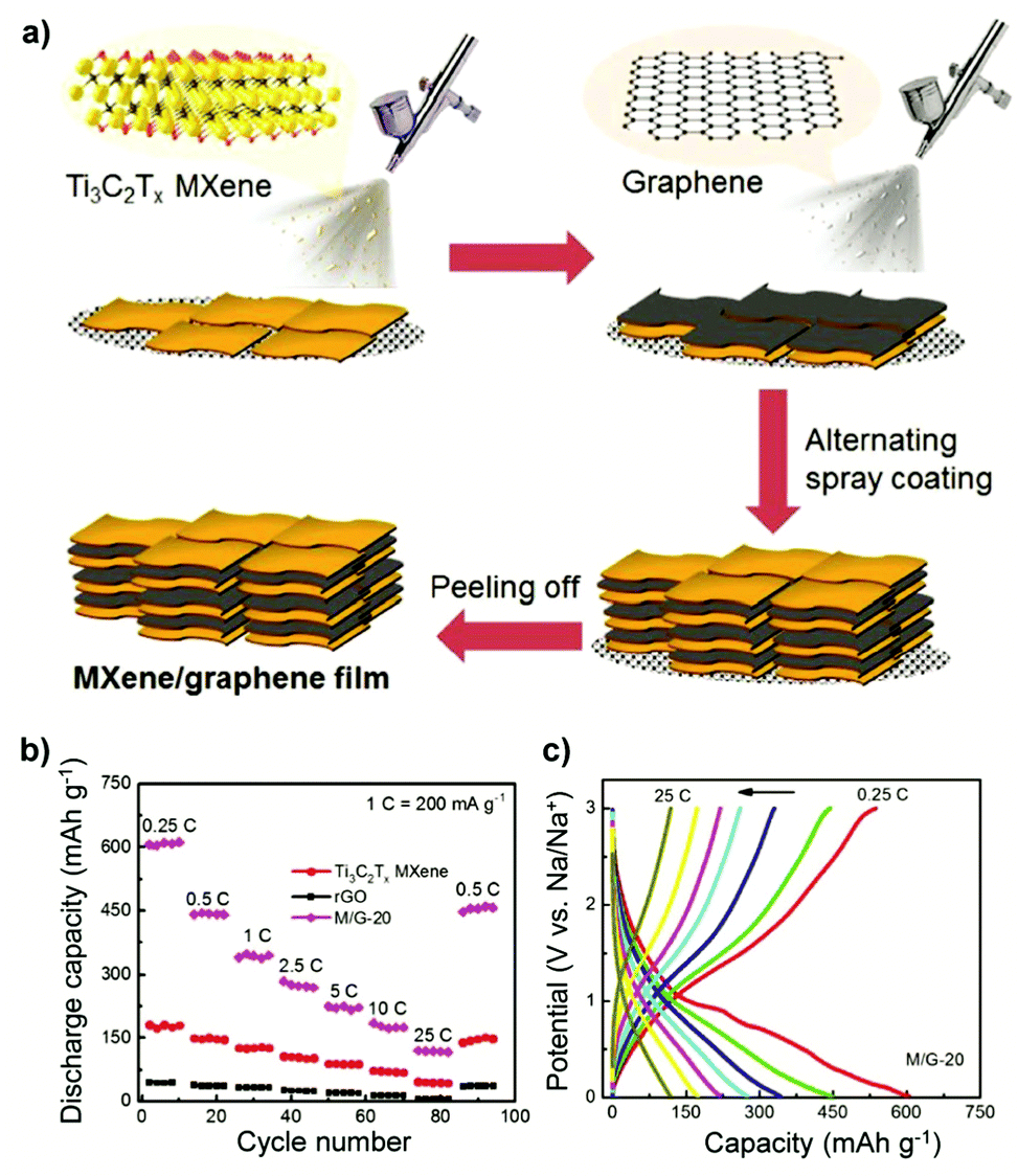 | ||
| Fig. 3 (a) Schematic representation of the manufacturing of free-standing and flexible 2D MXene/graphene heterostructured films by a spray-assisted LbL process. (b) Rate profiles. (c) Charge–discharge curves of the M/G-20 film at different current rates. Reproduced with permission.63 Copyright 2019, John Wiley and Sons. | ||
In an effort to further improve the homogeneity of spray coated films of 2D materials by facilitating the nebulisation of their inks, ultrasonic spraying systems have been developed.81 Unlike conventional pressure nozzles, ultrasonic nozzles utilise piezoelectric transducers to shear the solution and create a fine mist using ultrasonic vibrations. As a result, smaller monodisperse droplets can be achieved (2–20 μm), whose size can be modulated by adjusting the vibration frequency, increasing the resolution of the coating process and enhancing the homogeneity of the deposited films. This technology has found ample application in the production of hybrid perovskite solar cells, and specifically for the deposition of the perovskite layer, in combination with spin coating or thermal evaporation for the deposition of the electron and hole transport layers.82,83 In 2014 Lidzey et al. reported the fabrication of planar heterostructure CH3NH3PbI3xClx perovskite solar cells under ambient conditions with a peak power conversion efficiency (PCE) of 11%.84 The process involved dissolving perovskite precursors methylammonium iodide (MAI) and PbCl2 powder in DMF (a molar ratio of 3:1; total conc. 100 mg mL−1), and depositing this precursor ink in a single pass onto a heated pre-patterned glass ITO/PEDOT:PSS (30 nm layer, deposited by spin-coating) affording a dry film, which was later annealed to promote crystallisation of the perovskite.
Choi et al. further enhanced the control and definition of this deposition platform, developing a megasonic spray coating system for the manufacturing of large area hybrid organic–inorganic perovskite solar cells (Fig. 4).85 The spray system consisted of an ultrasonic nebuliser fitted with a plastic nozzle, attached to a moving arm allowing movement in the Y-axis. The substrate was placed on a heated stage capable of moving in the X-axis, allowing the continuous deposition of materials over a large area (56.25 cm2). While most ultrasonic spray systems work at frequencies below 1 MHz, the system reported by Choi operates at 1.7 MHz, generating homogeneous 2–4 μm droplets. A CH3NH3PbI3 precursor solution was deposited onto PEDOT:PSS coated glass/ITO using the megasonic spray system, yielding a highly uniform perovskite film after thermal treatment. The perovskite solar cell was fabricated by sequentially depositing via thermal evaporation: C60 (20 nm), bathocuproine (10 nm), and Cu (50 nm). The produced cell gave a peak PCE of 14.2% (with an average PCE of 13.7%), the highest among spray-coated large-area (i.e., active area of 10 mm2) perovskite solar cells.
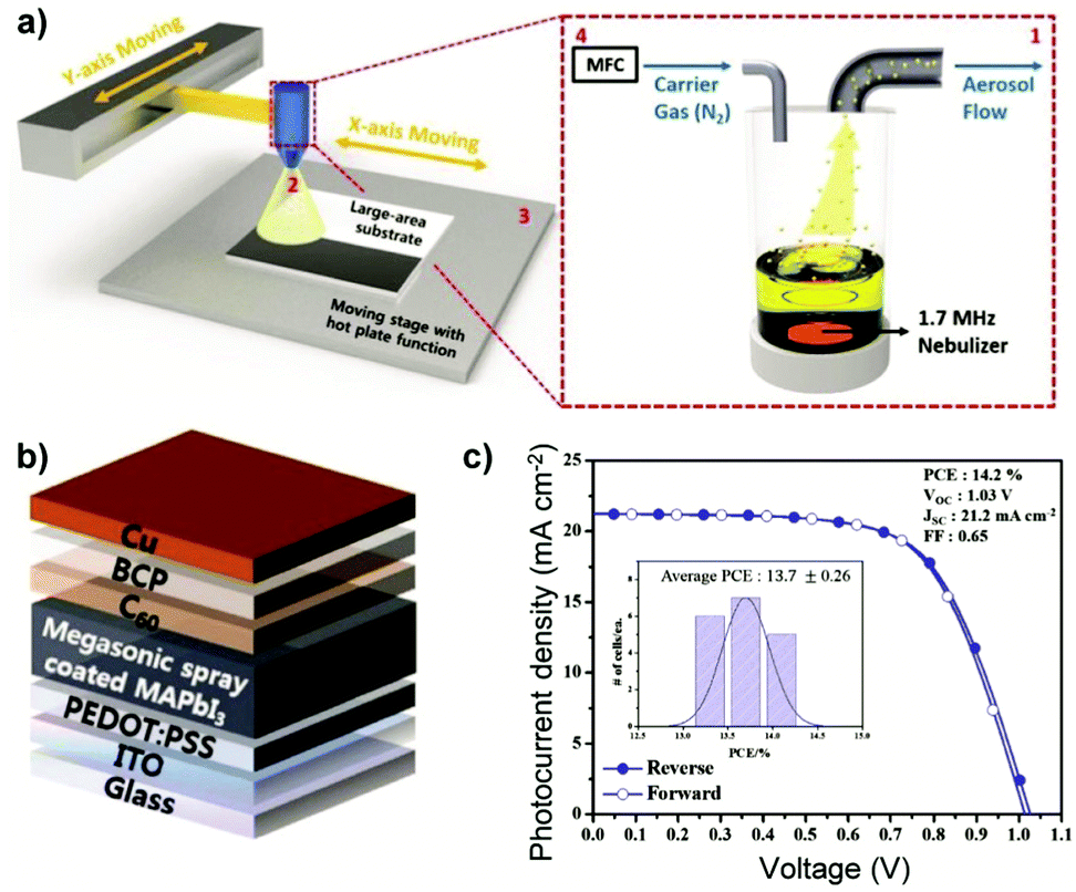 | ||
| Fig. 4 (a) Schematic representation of the megasonic spray-coating process. (b) Schematic illustration of an inverted planar MAPbI3 perovskite solar cell fabricated via the megasonic spray-coating system. (c) J–V curves and histogram (inset) of 18 megasonic sprayed perovskite solar cells with a 1 cm2 active area under one sun illumination. Reproduced with permission.85 Copyright 2018, John Wiley and Sons. | ||
Lidzey and coworkers ultimately developed an all spray coating-based process, consisting of the sequential deposition of tin oxide thin films, a triple-cation perovskite and spiro-OMeTAD (∼200 nm),64 drastically decreasing the overall production cost without affecting their efficiency (Fig. 5). On small-area substrates (2.5 mm2), the authors achieved a maximum reverse scan PCE of 19.4%, the highest reported to date, with an average PCE of 16.6 ± 2.4%. On large-area devices (15.4 mm2), 16.3% PCE was achieved, with an average of 10.3 ± 4.0%. In this case, the average PCE was hindered by the presence of structural defects in the active area of some devices, indicating that with further optimisation of the coating process higher PCEs could be achieved for this fully spray deposited devices.
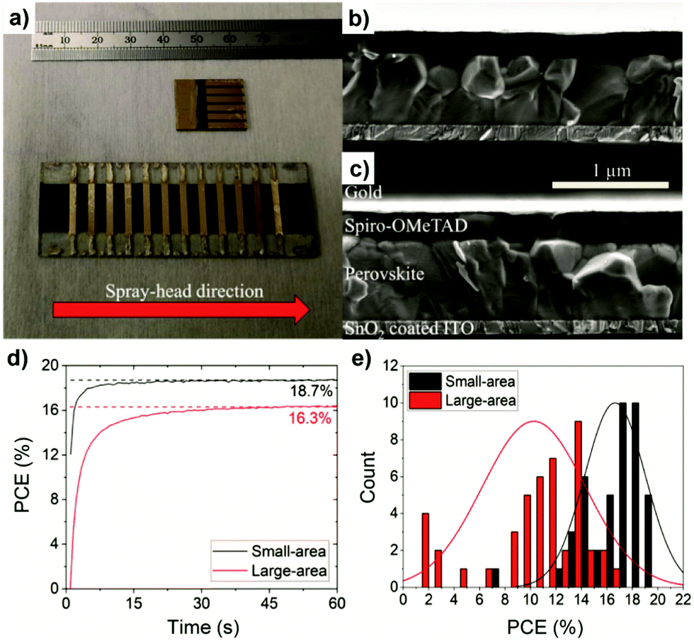 | ||
| Fig. 5 (a) Small and large-area fully spray-coated perovskite solar cells. (b) Cross-sectional SEM image of complete devices incorporating a spray-cast perovskite layer. The device in part (b) utilises spin cast SnO2 and spiro-OMeTAD layers whereas the device in part (c) is fully spray-coated. (d) Output power of the champion devices when held (for 60 s) at a fixed voltage close to the maximum power point. (e) Histogram of reverse-scan PCE data from 43 fully spray-cast small-area devices and 45 large-area devices. Reproduced with permission.64 Copyright 2020, Springer Nature. | ||
2.2 Inkjet printing
Inkjet printing is a digital non-contact printing technique vastly used in both research and industry, where ink droplets are jetted and deposited in fast succession onto a heated substrate to produce predesigned patterns without requiring a mask.46,79 Characterised by very low ink consumption (pL–μL drops, 1–2 mL; required viscosity: 4–30 mPa s; 2D material loading: 2–10 w%), this technology can provide an attractive route to the fabrication of complex heterostructures with high resolution (i.e., 10–200 μm), low cost, and large scale advantages.47,86,87 Based on the droplet generation mechanism, there are two main types of inkjet printing, continuous inkjet printing (C-IJP) and drop-on-demand inkjet printing (DOD-IJP).In a seminal report, Coleman and coworkers reported a hybrid process involving the inkjet printing of conductive graphene electrodes and spray coating of a dielectric h-BN layer with thicknesses ranging from 1.65 to 5.15 μm to produce all-printed capacitors. The devices displayed capacitances ranging from 0.24 to 1.1 nF cm−2, indicating the creation of pinhole-free films.88 Shortly after, the same group produced all printed transistors composed of vertically stacked nanosheet networks comprising a graphene source, drain, and gate electrodes; a TMD (i.e., MoS2, MoSe2, WS2, and WSe2) channel; and a h-BN separator. These devices displayed an ON/OFF current ratio of 6 × 10² and a mobility of 0.1 cm2 V−1 s−1.3 Torrisi et al. instead printed graphene h-BN field-effect transistors (FETs) on flexible polyester textiles (Fig. 6).65 Specifically, the graphene/h-BN textile FETs (80 × 500 μm) were produced by sequentially printing: a PEDOT:PSS film as the gate electrode (∼6.5 μm); a h-BN dielectric layer (∼2 μm, also responsible for smoothing the substrate's residual roughness); a thick graphene channel (∼200 nm); and finally PEDOT:PSS source and drain contacts (∼800 nm). Upon topological investigation, the layers became homogeneous, and did not present any visible pinhole or delaminating area. The average field-effect mobility of these flexible devices resulted in μh ∼ 91 ± 29 cm2 V−1 s−1 and μe ∼ 22 ± 10 cm2 V−1 s−1, respectively; whilst the ON/OFF current ratio was recorded to be 1.23 ± 0.3. Finally, thanks to a waterproof polyurethane protective layer on the textiles, these FETs proved resilient to water washings (>20 times, no significant degradation).
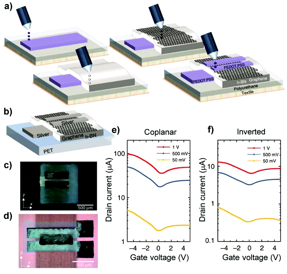 | ||
| Fig. 6 (a) Fabrication steps of the inkjet-printed inverted-staggered FET heterostructure on textile. (b) Schematic of a printed inverted-staggered FET heterostructure. (c) Inverted-staggered and (d) coplanar FET heterostructures on PET. (e and f) Transfer characteristics of the FETs as a function of Vds. Reproduced with permission.65 Copyright 2017, Springer Nature. | ||
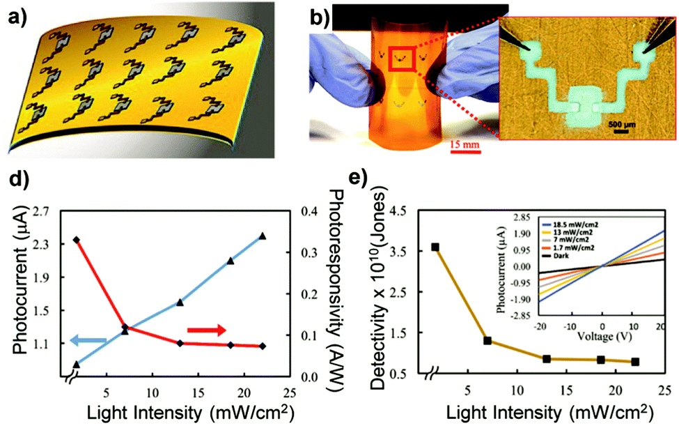
Casiraghi and Fiori et al. recently reported another hybrid combined CVD-inkjet printing approach for the production of high performance MoS2-based flexible FETs to exploit the higher control on the properties and purity of CVD grown 2D materials. After CVD growth, transfer of MoS2 onto the paper substrate and printing of the h-BN dielectric and silver source/drain contacts led to devices characterised by an ON/OFF current of 8 × 10³ and a mobility of 5.5 cm2 V−1 s−1.89 Beyond transistors, Casiraghi et al. formulated functional inkjet-optimised aqueous 2DM-based inks (i.e., graphene, MoS2, WS2 and h-BN), for the fabrication of fully inkjet-printed heterostructure-based photodetectors on paper showing a responsivity higher than 1 mA W−1 and the first ever printed programmable logic device.48 In the same year Kaul and coworkers printed graphene/MoS2 heterostructure-based flexible prosthetic devices comprising a photodetector as a therapeutic remedy for retinal tissue degradation (Fig. 7).90 The biocompatible devices (average 98% cellular viability on the printed substrates) were responsive to incoming broadband visible radiation, and generated a photocurrent that scaled proportionally with the intensity of incident light (photoresponsivity R ∼ 0.30 A W−1, and calculated detectivity D ∼ 3.6 × 10¹⁰ Jones).
 | ||
| Fig. 7 (a) Representation of the potential for scalability for printing 2D heterostructure devices for AMD over a large format using low-cost inkjet printing on flexible substrates. (b) An actual array of inkjet-printed heterostructure devices on a flexible polyimide film over an area of 60 × 50mm. Inset: A single inkjet-printed heterostructure device, where graphene electrodes were printed on top of the MoS2 layer. (c) The dependence of Iph and R on light intensity at 20V. (d) D as a function of light intensity at 20 V. Inset: I–V characteristics at various light intensities, where Iph is seen to increase linearly with light intensity. Reproduced with permission.90 Copyright 2017, Springer Nature. | ||
Fully inkjet-printed graphene/perovskite/graphene heterostructure-based photodetectors have been recently reported by He et al., achieving a photoresponsivity as high as ∼0.53 A W−1 and a detectivity of 3.4 × 10¹⁰ Jones in the visible range (400–700 nm) at room temperature.91 The devices were straightforwardly produced by initial patterned printing of a graphene layer as an interdigitated electrode on glass, followed by printing of a CH3NH3PbI3xClx perovskite precursor solution and in situ crystallisation (annealing at 90 °C in a N2 atmosphere).
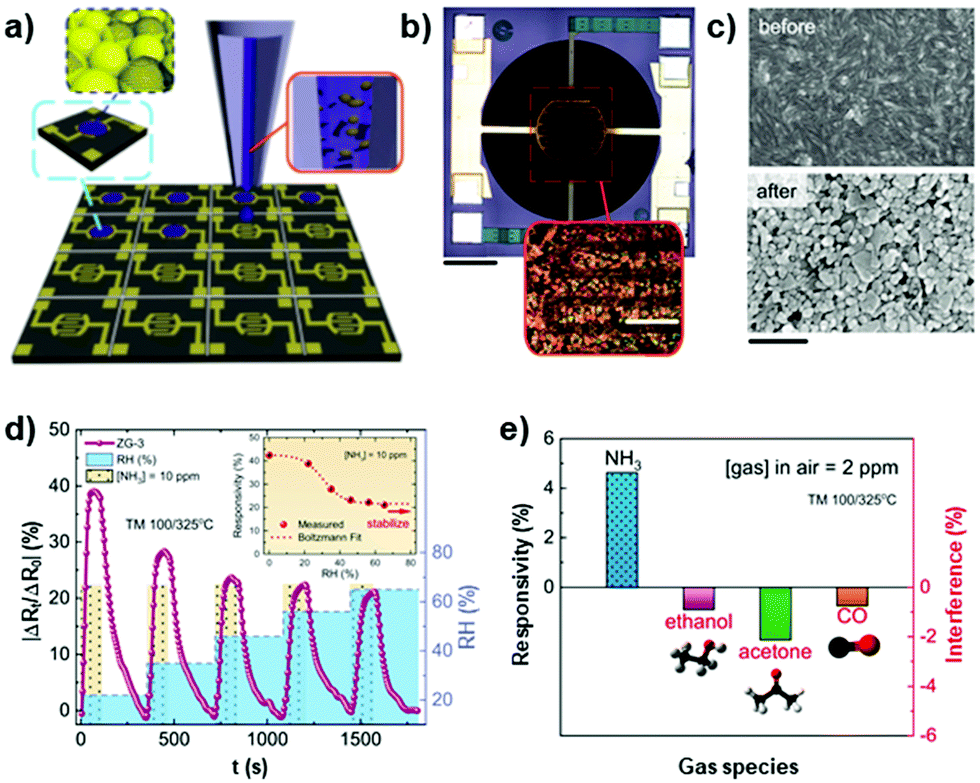
Hasan and coworkers reported the development of CMOS microplate (μHP)-integrated graphene/metaloxide breath sensors via inkjet printing, to swiftly (i.e., response and recovery time of 28 and 43 s, respectively) and promptly (i.e., responsivity of 1500% at 10 ppm pure NH3) detect NH3 in exhaled breath, a critical biomarker for a variety of kidney and liver conditions, with excellent cross-device and cross-cycle consistency (<0.5% and <0.41% variation in responsivity) and long-term stability (<1% variation).66 The miniaturised sensing platforms were readily produced by direct printing of a hybrid ZnO–graphene ink onto the electrodes of μHP (1 × 1 mm; Fig. 8); 20 passes gave the best condition to optimise trade-off between the uniformity of the printed film, conductivity and reaction/recovery time. This fabrication process enables automated fabrication of multiple devices at once, prompting scalability and device-to-device performance repeatability. Possible interference from acetone was compensated through the parallel deployment of inkjet-printed graphene/WO3 sensors (superior selectivity towards acetone).
 | ||
| Fig. 8 (a) Illustration of the inkjet deposition process. (b) Microscopic image of the inkjet-deposited CMOS sensory device. Scale bar 200 μm. Inset: Enlarged view: scale bar 20 μm. (c) SEM images of printed ZnO–graphene composite films: pre-annealing on the top, post-annealing on the bottom. Scale bar 250nm. (d) Normalized response at 120/240 s NH3 exposure/release cycles varied at various RH levels; (inset) responsivity as a function of RH levels. (e) Cross-analyte selectivity among common interfering gas species in exhaled breath. Reproduced with permission.66 Copyright 2019, Springer Nature. | ||
Lin, Li and coworkers extended the dimensionality of the inkjet printing technology by developing an innovative hybrid 3D freeze-inkjet printing method for the manufacture of a hybrid MoS2/graphene 3D porous aerogels (Fig. 9).92 The procedure described combines inkjet printing with freeze casting, exploiting the formation of ice microcrystals during printing to control both the microstructure and microporosity of the resulting macrostructure. A viscous aqueous ink was prepared by dispersing ammonium thiomolybdate (i.e., MoS2 precursor) and graphene oxide in deionised water. Following a template-directed approach, this ink was printed onto a Ni foam substrate held at −30 °C. The ice crystals formed during printing were further grown by placing the substrate in a freezer set at −70 °C for 24 h. The aerogel was hence recovered by removal of the ice template through freeze drying, followed by thermal treatment in an inert atmosphere (3% H2, 97% Ar, 2 h, 600 °C). Morphological investigations demonstrated that the hybrid aerogel consisted of MoS2 nanoparticles anchored on the surface of a porous reduced graphene oxide framework. When employed as a porous anode material for Na+ ion batteries it reported superior capacitance (∼429 – 800 mA h g−1) compared to carbon black/MoS2 powder electrodes mixed with a polyvinylidene difluoride binder (<200 mA h g−1) or a MoS2/reduced graphene oxide aerogel printed on a planar copper foil (<300 mA h g−1). Lastly, ten Elshof and collaborators reported this year the fabrication of all-inkjet printed solid-state sandwiched supercapacitors composed of Ti3C2Tx MXene nanosheets as electrodes, and graphene oxide as a solid-state electrolyte (MXene/GO/MXene; device thickness ∼4 μm),67 in which the proton diffusion is facilitated by the free H2O molecules trapped in the graphene oxide layer. The heterostructure-based supercapacitors present high areal capacitance (i.e., CA of 9.8 and 3 mF cm−2 at a current density of 40 μA cm−2, for 30 and 10 MXene layer electrodes respectively), which could be further increased by including liquid electrolytes in the structure, good cycling stability (i.e., ∼100% capacitance retention after 10000 cycles) and high areal energy (i.e., 0.49 μW h cm−2 at a PA of 12.55 μW cm−2 for a 30 MXene layer electrode), comparable with the existing printed supercapacitors.
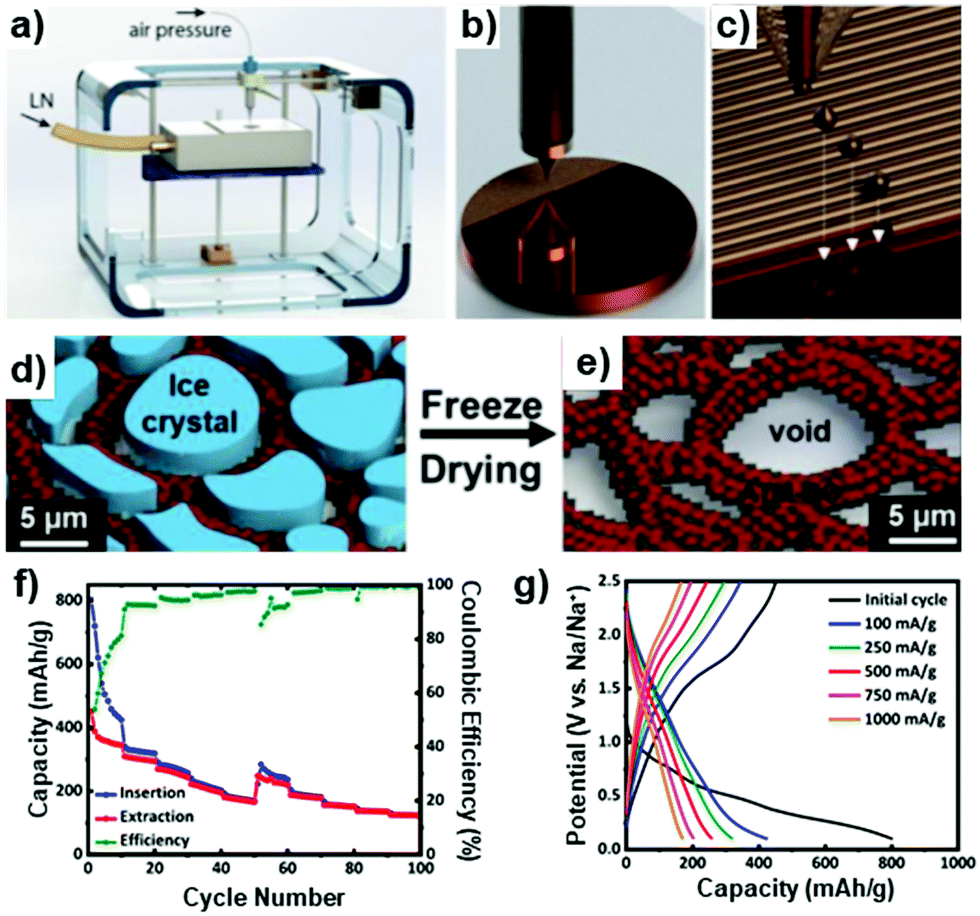 | ||
| Fig. 9 (a) Schematics of the 3D “drop-on-demand” ink jet printing setup. (b and c) Printing process of the ATM–GO droplets in a raster fashion. (d) Ice template formation during printing. (e) Resulting ATM–GO aerogel after freeze drying. (f) Rate performance at 5 different current density values. (g) Galvanostatic charge–discharge curves of the first cycle in comparison with those in the 10th cycle. Reproduced with permission.92 Copyright 2019, Elsevier. | ||
2.3 Extrusion-based 3D printing
Extrusion-based 3D printing is an additive manufacturing technology that offers the possibility of rapidly fabricating (i.e., hours) complex self-supporting three dimensional architectures with tuneable mechanical properties at low cost, with high precision (i.e., resolution: 50–200 μm) and close to zero waste.46,93,94 This technique employs a X,Y,Z-motion nozzle or stage to assemble 3D structures by extruding a continuous ink filament at room temperature in a layer-by-layer fashion, upon computerised control.95–97 The viscoelastic ink materials (i.e., viscosity: 5–500000 mPa s; 2D material loading: 12–40 w% rapid drying time; self-supporting) must present a shear thinning behaviour to facilitate the extrusion process, and enable shape retention after deposition.98,99
By careful design, printed 3D macrostructures of 2DMs can present enhanced mechanical properties, such as high stretchability and negative Poisson's ratio in the case of graphene,100,101 while retaining the inherent properties of the monolayers (e.g., high electrical/thermal conductivity, surface area, mechanical properties, etc.). Moreover, the applied axial force induced alignment of 2DMs during printing is beneficial for the formation of interconnected 3D networks fostering high thermal/electrical conductivity.95 This technology has for example enabled the development of highly stretchable graphene-based electronics,102 addressing the issue of conductivity loss of printed planar electronics under large deformations (i.e., low stretchability)103 avoiding the use of elastomeric polymers compromising conductivity.104,105
Worsley et al. reported in 2015 highly compressible lightweight graphene 3D printed aerogel microlattices, displaying supercompressibility (∼90% compressive strain) while maintaining the large surface area of single graphene sheets.106 These interconnected microporous architectures proved ideal (e.g., surface area enhancement, porosity, etc.) for integration in energy applications. Indeed, Worsley and Li et al. reported briefly after the printing of hybrid graphene oxide/graphene nanoplatelet/silica nanoparticle composite aerogel electrodes for supercapacitor applications.107 These lightweight, conductive porous electrodes exhibited significant electrochemical properties, and the produced supercapacitors (i.e., thickness mm range) displayed capacitive retentions (∼90% from 0.5 to 10 A g−1) and power densities (>4 kW kg−1) equal or superior to those of 10–100 times thinner devices. These results have recently been improved by the same authors, who reported the 3D printing of hybrid graphene/MnO2 porous electrodes favourable for electrolyte and ion diffusion, achieving a record areal capacitance of 44.13 F cm−2 and excellent capacitance normalised to area/gravimetry/volume, which is the trade-off for most electrodes (Fig. 10).108 These electrodes were produced by homogeneous electrodeposition of MnO2 onto a 3D printed graphene scaffold. The thick (i.e., 4 mm) hybrid electrodes reported presented high MnO2 loading (i.e., 182.2 mg cm−2), an increase in surface area upon electrodeposition and an almost 4-fold increase in areal capacitance compared to thinner devices (i.e., 44.13 F cm−2 and 11.55 F cm−2 at 0.5 mA cm−2 for 4 and 1 mm thick electrodes, respectively).
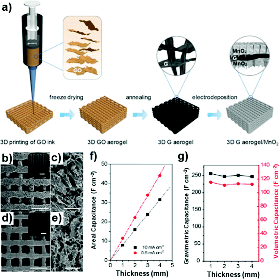 | ||
| Fig. 10 (a) Schematic illustration of fabrication of a 3D printed graphene aerogel/MnO2 electrode. (b) Top-view SEM image of a 3D printed graphene aerogel lattice. (c) Magnification of a cylindrical rod highlighted in (b). (d) Top-view SEM image of a 3D printed graphene aerogel lattice electrodeposited with MnO2 for 600 s. (e) Magnification of a cylindrical rod highlighted in (d). (f) Areal capacitance of the electrodes measured at 0.5 and 10 mA cm−2. (g) Gravimetric capacitance and volumetric capacitances as a function of electrode thickness. Reproduced with permission.108 Copyright 2019, Elsevier. | ||
Still in the field of energy related materials, Rocha, García-Tuñón and collaborators reported the multi-material 3D printing of hybrid graphene/Cu electrodes for energy storage.109 In this case both the active material (i.e., graphene oxide) and the current collector (i.e., Cu) precursors are formulated into inks and printed into the multicomponent electrode using two printing nozzles per layer. After printing, the electrodes were sequentially frozen (liquid N2), freeze-dried and thermally reduced, providing a self-standing binder-free interdigitated porous electrode (∼5 mm thick), characterised by specific energy and power density values of 26 W h kg−1 (at a power density of 1.7 kW kg−1) and 13 kW kg−1 (at an energy density of 1.2 W h kg−1), respectively. The capacitance retention at 15 A g−1 resulted in ∼80% after 10000 cycles, indicating promising viability and long-term stability.
For a different application, Fan et al. reported the printing of graphitic carbon nitride (g-C3N4) hybrid aerogel membranes with patterned macroscopic architectures to be employed in solar activated wastewater remediation processes (Fig. 11).68 The functional ink was formulated by mixing g-C3N4 nanosheets (CNNS) with sodium alginate (SA), to achieve correct viscosity and shear thinning behaviour. In the presence of multivalent cations (e.g., Ca2+), SA undergoes a fast gelation reaction by ionically cross-linking the linear chains, resulting in a hydrogel. The authors exploited this reaction to fully cross-link SA in the 3D printed samples by submerging the structures in a CaCl2 solution, followed by supercritical CO2 drying to afford the carbon nitride-based hybrid aerogel membranes, characterised by a surface area of 74.2 m2 g−1 (mean pore diameter 17.81 nm and volume 0.3303 cm3 g−1). These 3D printed aerogels were then explored for solar wastewater remediation by preparing a CNNS/SA/Au hybrid, in which cetyltrimethylammonium bromide (CTAB)-capped Au nanobipyramids (i.e., 1 wt%) were introduced in the aerogel to act as visible light sensitisers and cocatalysts. The ink was prepared in the same manner, by mixing CNNS/Au with SA. The solar wastewater remediation activity was evaluated by testing the methylene blue photodegradation under visible light irradiation (λ > 420 nm). This activity was compared to a contrast sample, prepared with the same ink and having equal surface area and mesoporosity, but without the 3D features. The 3D printed sample displayed a superior solar wastewater remediation activity (0.0322 min−1), about 2.5 times higher than the contrast sample, which can be explained by an increase in liquid velocity and dye diffusion. Furthermore, no noticeable decrease in activity was observed after three cycles.
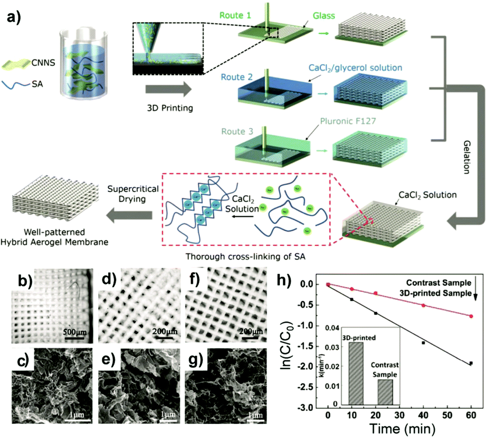 | ||
| Fig. 11 (a) Schematic illustration of the fabrication process. (b) Optical image of the CN–SA hybrid aerogel membrane printed directly in air and the cross-sectional SEM image (c). (d) Optical image showing the top view of the woodpile structure printed in a CaCl2/glycerol solution and the cross-sectional SEM image (e). (f) Optical image of a woodpile structure printed in Pluronic F127 and the cross-sectional SEM image (g). (h) Comparison of the photocatalytic MB degradation rates (λ > 420 nm). Reproduced with permission.68 Copyright 2018, John Wiley and Sons. | ||
3. Summary and prospects
The last decade has witnessed the conceptualisation and thriving of 2DM heterostructures, an exciting playground that stimulated the fantasy of researchers in creating exotic combinations of 2D materials in pursuit of high-performance synergistic outcomes. In this short perspective paper, we have introduced the readers to 2DM heterostructures emphasising their technological potential and the challenges they face with respect to their exploitation in end-user products. After briefly summarising the pioneering heterostructure fabrication processes, with their achievements and limitations, we then focused on discussing the recent progress in the automatised and reliable production of bespoke heterostructure-based devices exploiting solution processed 2DMs and industrially relevant manufacturing platforms, namely: spray coating, inkjet printing and extrusion-based 3D printing. As discussed in the previous section, these three technologies are the ones currently most investigated and promising for the production of 2DM heterostructures. All of these technologies allow high precision deposition of 2DM inks, when formulated in the appropriate 2D material loading/viscosity range (see Table 1, no 2DM related limitations). Moreover, these technologies complement each other: spray casting is better at delivering large area films of controlled thickness and roughness; inkjet, on the other hand, is better suited at tackling smaller yet sophisticated patterned architectures; and extrusion-based 3D printing can instead deliver shape-retaining self-supporting 3D architectures, eventually presenting enhanced mechanical properties, depending on the adopted design.| Spray coating | Inkjet printing | 3D printing | |
|---|---|---|---|
| 2DMs loading | 0.1–10 wt% | 2–10 wt% | 12–40 wt% |
| Viscosity | 1–1000 mPa s | 4–30 mPa s | 5–500000 mPa s |
| Resolution | 2–200 μm | 10–200 μm | 50–200 μm |
| Advantages | Fine-tuning over film thickness and roughness over large areas, speed | Advanced patterning capability | Tuning of the mechanical properties of the 3D structures, speed |
| Disadvantages | Low patterning resolution | Low speed | Low patterning resolution |
These established technologies, characterised by accessibility, low costs and low consumption merits, have developed adopting to the requirements of 2DM-based device production both in the hardware (e.g., ultrasonic nozzle for spray coaters, size of nozzles) and ink processing (e.g., passes, operative distances, roughness control, etc.), tackling critical controversies concerning the standardisation and prospective mass production of 2DM heterostructure products, achieving:
(I) Strict performance tailoring and control through automation: the development of fully automated (i.e., all sprayed/printed) production processes not only reduce manipulation steps and production time, but facilitate the controlled (e.g., thickness, roughness, pattern, etc.) and reproducible ordered deposition of 2DMs with high-resolution merits. This control results in the standardisation of the products and of their performances, enabling the definition of defined structure–property correlations underpinning their performance, to be later employed for the design of application-tailored highly efficient 2DM heterostructures.
(II) Enhanced production sustainability: compared to conventional energy intensive and waste producing manufacturing processes (e.g., CVD requiring high temperature and vacuum, several etching steps, etc.), the manufacturing technologies discussed in this perspective do not operate under fringe conditions, and most importantly do not produce waste. The material needed for the production of the heterostructure is sprayed/printed on demand where needed, without misuse. These inherent technological advantages, combined with novel formulation (e.g., volatile solvents, conscious fillers, additives, etc.) and synthetic paradigms (i.e., synthesis of 2DMs from industrial waste, as bio-based graphene synthesised from lignin recovered from the paper manufacturing industry) will play an important role in further reducing the ecological footprint of this technology.
(III) Scale-up at reduced costs: as mentioned previously, these technologies have already been optimised to satisfy the stringent cost control required in high-volume manufacturing landscapes.
The exciting results achieved hint at the disruptive potential this approach entails, yet further improvements in controlling the manufacturing processes are still needed, and commercialisation will benefit from the standardisation of quality and performance facilitated by these technologies. However, in combination with the improvement of the manufacturing platforms and processes, researchers are also still tackling the absence of standardised, scalable production processes for monolayered materials, which also play a crucial role in the creation of precisely controlled hybrid architectures, and tailoring of their structure/interface-dependent unique properties. Indeed, a consistent and high-yield production methodology for individual, large-area, atomically defined 2DM building blocks is currently still unavailable. Further research on the optimisation of the current top-down solution processing methodologies (e.g., homogenisation), the adaptation of established bottom-up synthetic methodologies (i.e., CVD) or the development of novel inexpensive bottom-up synthetic methodologies for 2D monolayered materials (e.g., a chemical approach for 2D polymers, COFs, etc.) are required in order to achieve highly performant functional inks.
With the acceleration and establishment of reliable, cost-effective, large-volume fabrication methods for 2DM heterostructures and the expected quality enhancement of the exfoliated 2DMs, the most conceivable roadmap for the technological exploitation of 2DM heterostructures is inevitably intertwining and accelerated by that of single 2D materials. As forecast for graphene,25 it is highly probable that 2DM heterostructure-based technologies will not abruptly disrupt the market, but rather mature within niche applications for which these hybrids will offer unique advantages. The automatised high-throughput production technologies involved will most probably jump-start 2DM heterostructure market integration (i.e., current decade), targeting directly medium-sized markets (e.g., automatised and standardised production) bringing upon radical innovations in the development of marketable 2D material-based devices (e.g., printable electronics, photovoltaics, energy storage, sensing, etc.).
Author contributions
LM contributed to the conceptualisation of the message brought forward by this perspective article, the literature search supporting it and its writing. RF contributed to the literature search reviewed in this perspective, writing and editing of the images present in this manuscript.Conflicts of interest
There are no conflicts to declare.Acknowledgements
LM and RF gratefully acknowledge the University of Vienna for financial support, and the European Union's Horizon 2020 research and innovation programme for funding under the Marie Skłodowska-Curie grant agreement no. 101008237 – VIT (polymer engineering via molecular design: embedding electrical and optical properties into VITrimers). The authors thank Dr Vivek Wakchaure for discussion.Notes and references
- K. S. Novoselov, A. K. Geim, S. V. Morozov, D. Jiang, Y. Zhang, S. V. Dubonos, I. V. Grigorieva and A. A. Firsov, Science, 2004, 306, 666–669 CrossRef CAS PubMed.
- S. Z. Butler, S. M. Hollen, L. Cao, Y. Cui, J. A. Gupta, H. R. Gutiérrez, T. F. Heinz, S. S. Hong, J. Huang, A. F. Ismach, E. Johnston-Halperin, M. Kuno, V. V. Plashnitsa, R. D. Robinson, R. S. Ruoff, S. Salahuddin, J. Shan, L. Shi, M. G. Spencer, M. Terrones, W. Windl and J. E. Goldberger, ACS Nano, 2013, 7, 2898–2926 CrossRef CAS PubMed.
- A. G. Kelly, T. Hallam, C. Backes, A. Harvey, A. S. Esmaeily, I. Godwin, J. Coelho, V. Nicolosi, J. Lauth, A. Kulkarni, S. Kinge, L. D. A. Siebbeles, G. S. Duesberg and J. N. Coleman, Science, 2017, 356, 69–73 CrossRef CAS PubMed.
- Z. Zhang, X. Liu, J. Yu, Y. Hang, Y. Li, Y. Guo, Y. Xu, X. Sun, J. Zhou and W. Guo, Wiley Interdiscip. Rev.: Comput. Mol. Sci., 2016, 6, 324–350 CAS.
- M. Naguib and Y. Gogotsi, Acc. Chem. Res., 2015, 48, 128–135 CrossRef CAS PubMed.
- H. Zhang, ACS Nano, 2015, 9, 9451–9469 CrossRef CAS PubMed.
- M. Xu, T. Liang, M. Shi and H. Chen, Chem. Rev., 2013, 113, 3766–3798 CrossRef CAS PubMed.
- A. K. Geim and K. S. Novoselov, Nat. Mater., 2007, 6, 183–191 CrossRef CAS PubMed.
- C. Lee, X. Wei, J. W. Kysar and J. Hone, Science, 2008, 321, 385–388 CrossRef CAS PubMed.
- F. Bonaccorso, Z. Sun, T. Hasan and A. C. Ferrari, Nat. Photonics, 2010, 4, 611–622 CrossRef CAS.
- S. Bertolazzi, J. Brivio and A. Kis, ACS Nano, 2011, 5, 9703–9709 CrossRef CAS PubMed.
- W. Choi, N. Choudhary, G. H. Han, J. Park, D. Akinwande and Y. H. Lee, Mater. Today, 2017, 20, 116–130 CrossRef CAS.
- K. F. Mak, C. Lee, J. Hone, J. Shan and T. F. Heinz, Phys. Rev. Lett., 2010, 105, 136805 CrossRef PubMed.
- C. R. Dean, A. F. Young, I. Meric, C. Lee, L. Wang, S. Sorgenfrei, K. Watanabe, T. Taniguchi, P. Kim, K. L. Shepard and J. Hone, Nat. Nanotechnol., 2010, 5, 722–726 CrossRef CAS PubMed.
- J. Xue, J. Sanchez-Yamagishi, D. Bulmash, P. Jacquod, A. Deshpande, K. Watanabe, T. Taniguchi, P. Jarillo-Herrero and B. J. Leroy, Nat. Mater., 2011, 10, 282–285 CrossRef CAS PubMed.
- K. Watanabe, T. Taniguchi and H. Kanda, Nat. Mater., 2004, 3, 404–409 CrossRef CAS PubMed.
- A. Falin, Q. Cai, E. J. G. Santos, D. Scullion, D. Qian, R. Zhang, Z. Yang, S. Huang, K. Watanabe, T. Taniguchi, M. R. Barnett, Y. Chen, R. S. Ruoff and L. H. Li, Nat. Commun., 2017, 8, 15815 CrossRef CAS PubMed.
- B. Deng, V. Tran, Y. Xie, H. Jiang, C. Li, Q. Guo, X. Wang, H. Tian, S. J. Koester, H. Wang, J. J. Cha, Q. Xia, L. Yang and F. Xia, Nat. Commun., 2017, 8, 14474 CrossRef CAS PubMed.
- V. Tran, R. Soklaski, Y. Liang and L. Yang, Phys. Rev. B: Condens. Matter Mater. Phys., 2014, 89, 235319 CrossRef.
- H. Kim and H. N. Alshareef, ACS Mater. Lett., 2020, 2, 55–70 CrossRef CAS.
- Y. Liu, H. Xiao and W. A. Goddard, J. Am. Chem. Soc., 2016, 138, 15853–15856 CrossRef CAS PubMed.
- M. Khazaei, M. Arai, T. Sasaki, A. Ranjbar, Y. Liang and S. Yunoki, Phys. Rev. B: Condens. Matter Mater. Phys., 2015, 92, 75411 CrossRef.
- A. Lipatov, H. Lu, M. Alhabeb, B. Anasori, A. Gruverman, Y. Gogotsi and A. Sinitskii, Sci. Adv., 2018, 4, eaat0491 CrossRef PubMed.
- Moving towards the market, Nat. Mater., 2019, 18(6), 519 DOI:10.1038/s41563-019-0394-4.
- D. Neumaier, S. Pindl and M. C. Lemme, Nat. Mater., 2019, 18, 525–529 CrossRef CAS PubMed.
- N. R. Glavin, R. Rao, V. Varshney, E. Bianco, A. Apte, A. Roy, E. Ringe and P. M. Ajayan, Adv. Mater., 2020, 32, 1904302 CrossRef CAS PubMed.
- K. Khan, A. K. Tareen, M. Aslam, R. Wang, Y. Zhang, A. Mahmood, Z. Ouyang, H. Zhang and Z. Guo, J. Mater. Chem. C, 2020, 8, 387–440 RSC.
- C. Tan, X. Cao, X. J. Wu, Q. He, J. Yang, X. Zhang, J. Chen, W. Zhao, S. Han, G. H. Nam, M. Sindoro and H. Zhang, Chem. Rev., 2017, 117, 6225–6331 CrossRef CAS PubMed.
- A. C. Ferrari, F. Bonaccorso, V. Fal’ko, K. S. Novoselov, S. Roche, P. Bøggild, S. Borini, F. H. L. Koppens, V. Palermo, N. Pugno, J. A. Garrido, R. Sordan, A. Bianco, L. Ballerini, M. Prato, E. Lidorikis, J. Kivioja, C. Marinelli, T. Ryhänen, A. Morpurgo, J. N. Coleman, V. Nicolosi, L. Colombo, A. Fert, M. Garcia-Hernandez, A. Bachtold, G. F. Schneider, F. Guinea, C. Dekker, M. Barbone, Z. Sun, C. Galiotis, A. N. Grigorenko, G. Konstantatos, A. Kis, M. Katsnelson, L. Vandersypen, A. Loiseau, V. Morandi, D. Neumaier, E. Treossi, V. Pellegrini, M. Polini, A. Tredicucci, G. M. Williams, B. Hee Hong, J. H. Ahn, J. Min Kim, H. Zirath, B. J. Van Wees, H. Van Der Zant, L. Occhipinti, A. Di Matteo, I. A. Kinloch, T. Seyller, E. Quesnel, X. Feng, K. Teo, N. Rupesinghe, P. Hakonen, S. R. T. Neil, Q. Tannock, T. Löfwander and J. Kinaret, Nanoscale, 2015, 7, 4598–4810 RSC.
- M. Zeng, Y. Xiao, J. Liu, K. Yang and L. Fu, Chem. Rev., 2018, 118, 6236–6296 CrossRef CAS PubMed.
- P. Solís-Fernández, M. Bissett and H. Ago, Chem. Soc. Rev., 2017, 46, 4572–4613 RSC.
- Y. Liu, N. O. Weiss, X. X. Duan, H. C. Cheng, Y. Huang and X. X. Duan, Nat. Rev. Mater., 2016, 1, 16042 CrossRef CAS.
- J. Su, G. Li, X.-H. Li and J.-S. Chen, Adv. Sci., 2019, 6, 1801702 CrossRef PubMed.
- G. H. Lee, Y. J. Yu, X. Cui, N. Petrone, C. C. H. Lee, M. S. Choi, D. Y. Lee, C. C. H. Lee, W. J. Yoo, K. Watanabe, T. Taniguchi, C. Nuckolls, P. Kim and J. Hone, ACS Nano, 2013, 7, 7931–7936 CrossRef CAS PubMed.
- E. Pomerantseva and Y. Gogotsi, Nat. Energy, 2017, 2, 17089 CrossRef CAS.
- F. Shahzad, M. Alhabeb, C. B. Hatter, B. Anasori, S. Man Hong, C. M. Koo and Y. Gogotsi, Science, 2016, 353, 1137–1140 CrossRef CAS PubMed.
- K. S. Novoselov, A. Mishchenko, A. Carvalho and A. H. Castro Neto, Science, 2016, 353, aac9439 CrossRef CAS PubMed.
- S. Das, J. A. Robinson, M. Dubey, H. Terrones and M. Terrones, Annu. Rev. Mater. Res., 2015, 45, 1–27 CrossRef CAS.
- X. Huang, C. Tan, Z. Yin and H. Zhang, Adv. Mater., 2014, 26, 2185–2204 CrossRef CAS PubMed.
- H. Wang, F. Liu, W. Fu, Z. Fang, W. Zhou and Z. Liu, Nanoscale, 2014, 6, 12250–12272 RSC.
- A. K. Geim and I. V. Grigorieva, Nature, 2013, 499, 419–425 CrossRef CAS PubMed.
- A. Quellmalz, X. Wang, S. Sawallich, B. Uzlu, M. Otto, S. Wagner, Z. Wang, M. Prechtl, O. Hartwig, S. Luo, G. S. Duesberg, M. C. Lemme, K. B. Gylfason, N. Roxhed, G. Stemme and F. Niklaus, Nat. Commun., 2021, 12, 917 CrossRef CAS PubMed.
- F. Withers, H. Yang, L. Britnell, A. P. Rooney, E. Lewis, A. Felten, C. R. Woods, V. Sanchez Romaguera, T. Georgiou, A. Eckmann, Y. J. Kim, S. G. Yeates, S. J. Haigh, A. K. Geim, K. S. Novoselov and C. Casiraghi, Nano Lett., 2014, 14, 3987–3992 CrossRef CAS PubMed.
- S. Witomska, T. Leydecker, A. Ciesielski and P. Samorì, Adv. Funct. Mater., 2019, 29, 1901126 CrossRef.
- X. Cai, Y. Luo, B. Liu and H.-M. Cheng, Chem. Soc. Rev., 2018, 47, 6224–6266 RSC.
- K. Hassan, M. J. Nine, T. T. Tung, N. Stanley, P. L. Yap, H. Rastin, L. Yu and D. Losic, Nanoscale, 2020, 12, 19007–19042 RSC.
- G. Hu, J. Kang, L. W. T. Ng, X. Zhu, R. C. T. Howe, C. G. Jones, M. C. Hersam and T. Hasan, Chem. Soc. Rev., 2018, 47, 3265–3300 RSC.
- D. McManus, S. Vranic, F. Withers, V. Sanchez-Romaguera, M. Macucci, H. Yang, R. Sorrentino, K. Parvez, S. K. Son, G. Iannaccone, K. Kostarelos, G. Fiori and C. Casiraghi, Nat. Nanotechnol., 2017, 12, 343–350 CrossRef CAS PubMed.
- J. N. Coleman, M. Lotya, A. O’Neill, S. D. Bergin, P. J. King, U. Khan, K. Young, A. Gaucher, S. De, R. J. Smith, I. V. Shvets, S. K. Arora, G. Stanton, H. Y. Kim, K. Lee, G. T. Kim, G. S. Duesberg, T. Hallam, J. J. Boland, J. J. Wang, J. F. Donegan, J. C. Grunlan, G. Moriarty, A. Shmeliov, R. J. Nicholls, J. M. Perkins, E. M. Grieveson, K. Theuwissen, D. W. McComb, P. D. Nellist and V. Nicolosi, Science, 2011, 331, 568–571 CrossRef CAS PubMed.
- R. Howe, Printing with graphene: exploring the inks set to unleash graphene's potential, https://www.mewburn.com/news-insights/printing-with-graphene-unleashing-graphenes-potential-through-mass-production.
- E. Pomerantseva and Y. Gogotsi, Nat. Energy, 2017, 2, 17089 CrossRef CAS.
- F. H. L. Koppens, T. Mueller, P. Avouris, A. C. Ferrari, M. S. Vitiello and M. Polini, Nat. Nanotechnol., 2014, 9, 780–793 CrossRef CAS PubMed.
- B. V. Lotsch, Annu. Rev. Mater. Res., 2015, 45, 85–109 CrossRef CAS.
- M. Y. Li, C. H. Chen, Y. Shi and L. J. Li, Mater. Today, 2016, 19, 322–335 CrossRef CAS.
- J. Lee, J.-H. Shin, G.-H. Lee and C.-H. Lee, Nanomaterials, 2016, 6, 193 CrossRef PubMed.
- F. Di Maria, M. Zangoli, I. E. Palam, E. Fabiano, A. Zanelli, M. Monari, A. Perinot, M. Caironi, V. Maiorano, A. Maggiore, M. Pugliese, E. Salatelli, G. Gigli, I. Viola and G. Barbarella, Adv. Funct. Mater., 2016, 26, 6970–6984 CrossRef CAS.
- D. L. Duong, S. J. Yun and Y. H. Lee, ACS Nano, 2017, 11, 11803–11830 CrossRef CAS PubMed.
- I. V. Sankar, J. Jeon, S. K. Jang, J. H. Cho, E. Hwang and S. Lee, NANO, 2019, 14, 1930009 CrossRef CAS.
- H. Liu, L. Li, M. E. Scofield and S. S. Wong, APL Mater., 2015, 3, 080701 CrossRef.
- F. Shahzad, M. Alhabeb, C. B. Hatter, B. Anasori, S. Man Hong, C. M. Koo and Y. Gogotsi, Science, 2016, 353, 1137–1140 CrossRef CAS PubMed.
- K. S. Novoselov, A. Mishchenko, A. Carvalho and A. H. Castro Neto, Science, 2016, 353, 461 CrossRef CAS PubMed.
- S. H. Bae, H. Kum, W. Kong, Y. Kim, C. Choi, B. Lee, P. Lin, Y. Park and J. Kim, Nat. Mater., 2019, 18, 550–560 CrossRef CAS PubMed.
- M. Zhao, N. Trainor, C. E. Ren, M. Torelli, B. Anasori and Y. Gogotsi, Adv. Mater. Technol., 2019, 4, 1800639 CrossRef.
- J. E. Bishop, C. D. Read, J. A. Smith, T. J. Routledge and D. G. Lidzey, Sci. Rep., 2020, 10, 6610 CrossRef CAS PubMed.
- T. Carey, S. Cacovich, G. Divitini, J. Ren, A. Mansouri, J. M. Kim, C. Wang, C. Ducati, R. Sordan and F. Torrisi, Nat. Commun., 2017, 8, 1202 CrossRef PubMed.
- T.-C. Wu, A. De Luca, Q. Zhong, X. Zhu, O. Ogbeide, D.-S. Um, G. Hu, T. Albrow-Owen, F. Udrea and T. Hasan, npj 2D Mater. Appl., 2019, 3, 42 CrossRef.
- Y. Wang, M. Mehrali, Y.-Z. Zhang, M. A. Timmerman, B. A. Boukamp, P.-Y. Xu and J. E. ten Elshof, Energy Storage Mater., 2021, 36, 318–325 CrossRef.
- P. He, X. Tang, L. Chen, P. Xie, L. He, H. Zhou, D. Zhang and T. Fan, Adv. Funct. Mater., 2018, 28, 1801121 CrossRef.
- Y. Shi, M. Osada, Y. Ebina and T. Sasaki, ACS Nano, 2020, 14, 15216–15226 CrossRef PubMed.
- G. Hu, T. Albrow-Owen, X. Jin, A. Ali, Y. Hu, R. C. T. Howe, K. Shehzad, Z. Yang, X. Zhu, R. I. Woodward, T.-C. Wu, H. Jussila, J.-B. Wu, P. Peng, P.-H. Tan, Z. Sun, E. J. R. Kelleher, M. Zhang, Y. Xu and T. Hasan, Nat. Commun., 2017, 8, 278 CrossRef PubMed.
- V. Bianchi, T. Carey, L. Viti, L. Li, E. H. Linfield, A. G. Davies, A. Tredicucci, D. Yoon, P. G. Karagiannidis, L. Lombardi, F. Tomarchio, A. C. Ferrari, F. Torrisi and M. S. Vitiello, Nat. Commun., 2017, 8, 15763 CrossRef CAS PubMed.
- E. B. Secor, P. L. Prabhumirashi, K. Puntambekar, M. L. Geier and M. C. Hersam, J. Phys. Chem. Lett., 2013, 4, 1347–1351 CrossRef CAS PubMed.
- K. Hassan, T. T. Tung, N. Stanley, P. L. Yap, F. Farivar, H. Rastin, M. J. Nine and D. Losic, Nanoscale, 2021, 13, 5356–5368 RSC.
- A. Moridi, S. M. Hassani-Gangaraj, M. Guagliano and M. Dao, Surf. Eng., 2014, 30, 369–395 CrossRef CAS.
- G. Cummins and M. P. Y. Desmulliez, Circuit World, 2012, 38, 193–213 CrossRef CAS.
- X. Tian, J. Jin, S. Yuan, C. K. Chua, S. B. Tor and K. Zhou, Adv. Energy Mater., 2017, 7, 1700127 CrossRef.
- L. Huang, Y. Huang, J. Liang, X. Wan and Y. Chen, Nano Res., 2011, 4, 675–684 CrossRef CAS.
- T. Carey, C. Jones, F. Le Moal, D. Deganello and F. Torrisi, ACS Appl. Mater. Interfaces, 2018, 10, 19948–19956 CrossRef CAS PubMed.
- S. Abdolhosseinzadeh, X. Jiang, H. Zhang, J. Qiu and C. (John) Zhang, Mater. Today, 2021, 48, 214–240 CrossRef CAS.
- S. Gilje, S. Han, M. Wang, K. L. Wang and R. B. Kaner, Nano Lett., 2007, 7, 3394–3398 CrossRef CAS PubMed.
- S. Das, B. Yang, G. Gu, P. C. Joshi, I. N. Ivanov, C. M. Rouleau, T. Aytug, D. B. Geohegan and K. Xiao, ACS Photonics, 2015, 2, 680–686 CrossRef CAS.
- J. E. Bishop, J. A. Smith, C. Greenland, V. Kumar, N. Vaenas, O. S. Game, T. J. Routledge, M. Wong-Stringer, C. Rodenburg and D. G. Lidzey, ACS Appl. Mater. Interfaces, 2018, 10, 39428–39434 CrossRef CAS PubMed.
- S. Ulična, B. Dou, D. H. Kim, K. Zhu, J. M. Walls, J. W. Bowers and M. F. A. M. Van Hest, ACS Appl. Energy Mater., 2018, 1, 1853–1857 CrossRef.
- A. T. Barrows, A. J. Pearson, C. K. Kwak, A. D. F. Dunbar, A. R. Buckley and D. G. Lidzey, Energy Environ. Sci., 2014, 7, 2944–2950 RSC.
- M. Park, W. Cho, G. Lee, S. C. Hong, M. Kim, J. Yoon, N. Ahn and M. Choi, Small, 2019, 15, 1804005 CrossRef PubMed.
- A. G. Ricciardulli and P. W. M. Blom, Adv. Mater. Technol., 2020, 5, 1900972 CrossRef CAS.
- I. Burgués-Ceballos, M. Stella, P. Lacharmoise and E. Martínez-Ferrero, J. Mater. Chem. A, 2014, 2, 17711–17722 RSC.
- A. G. Kelly, D. Finn, A. Harvey, T. Hallam and J. N. Coleman, Appl. Phys. Lett., 2016, 109, 23107 CrossRef.
- S. Conti, L. Pimpolari, G. Calabrese, R. Worsley, S. Majee, D. K. Polyushkin, M. Paur, S. Pace, D. H. Keum, F. Fabbri, G. Iannaccone, M. Macucci, C. Coletti, T. Mueller, C. Casiraghi and G. Fiori, Nat. Commun., 2020, 11, 3566 CrossRef CAS PubMed.
- R. F. Hossain, I. G. Deaguero, T. Boland and A. B. Kaul, npj 2D Mater. Appl., 2017, 1, 28 CrossRef.
- A. M. Alamri, S. Leung, M. Vaseem, A. Shamim and J. H. He, IEEE Trans. Electron Devices, 2019, 66, 2657–2661 CAS.
- E. Brown, P. Yan, H. Tekik, A. Elangovan, J. Wang, D. Lin and J. Li, Mater. Des., 2019, 170, 107689 CrossRef CAS.
- R. Yang, J. Zhou, C. Yang, L. Qiu and H. Cheng, Adv. Mater. Technol., 2020, 5, 1901066 CrossRef CAS.
- D. Ponnamma, Y. Yin, N. Salim, J. Parameswaranpillai, S. Thomas and N. Hameed, Composites, Part B, 2021, 204, 108493 CrossRef CAS.
- R. Yang, J. Zhou, C. Yang, L. Qiu and H. Cheng, Adv. Mater. Technol., 2020, 5, 1901066 CrossRef CAS.
- K. Hassan, M. J. Nine, T. T. Tung, N. Stanley, P. L. Yap, H. Rastin, L. Yu and D. Losic, Nanoscale, 2020, 12, 19007–19042 RSC.
- D. Ponnamma, Y. Yin, N. Salim, J. Parameswaranpillai, S. Thomas and N. Hameed, Composites, Part B, 2021, 204, 108493 CrossRef CAS.
- J. E. Smay, G. M. Gratson, R. F. Shepherd, J. Cesarano and J. A. Lewis, Adv. Mater., 2002, 14, 1279–1283 CrossRef CAS.
- C. Zhu and J. E. Smay, J. Rheol., 2011, 55, 655–672 CrossRef CAS.
- F. Guo, Y. Jiang, Z. Xu, Y. Xiao, B. Fang, Y. Liu, W. Gao, P. Zhao, H. Wang and C. Gao, Nat. Commun., 2018, 9, 881 CrossRef PubMed.
- H. Guo, R. Lv and S. Bai, Nano Mater. Sci., 2019, 1, 101–115 CrossRef.
- J. T. Muth, D. M. Vogt, R. L. Truby, Y. Mengüç, D. B. Kolesky, R. J. Wood and J. A. Lewis, Adv. Mater., 2014, 26, 6307–6312 CrossRef CAS PubMed.
- K. S. Kim, Y. Zhao, H. Jang, S. Y. Lee, J. M. Kim, K. S. Kim, J. H. Ahn, P. Kim, J. Y. Choi and B. H. Hong, Nature, 2009, 457, 706–710 CrossRef CAS PubMed.
- E. B. Secor, S. Lim, H. Zhang, C. D. Frisbie, L. F. Francis and M. C. Hersam, Adv. Mater., 2014, 26, 4533–4538 CrossRef CAS PubMed.
- Y. Cai, J. Shen, Z. Dai, X. Zang, Q. Dong, G. Guan, L. J. Li, W. Huang and X. Dong, Adv. Mater., 2017, 29, 1606411 CrossRef PubMed.
- C. Zhu, T. Y. J. Han, E. B. Duoss, A. M. Golobic, J. D. Kuntz, C. M. Spadaccini and M. A. Worsley, Nat. Commun., 2015, 6, 6962 CrossRef CAS PubMed.
- C. Zhu, T. Liu, F. Qian, T. Y. J. Han, E. B. Duoss, J. D. Kuntz, C. M. Spadaccini, M. A. Worsley and Y. Li, Nano Lett., 2016, 16, 3448–3456 CrossRef CAS PubMed.
- B. Yao, S. Chandrasekaran, J. Zhang, W. Xiao, F. Qian, C. Zhu, E. B. Duoss, C. M. Spadaccini, M. A. Worsley and Y. Li, Joule, 2019, 3, 459–470 CrossRef CAS.
- V. G. Rocha, E. García-Tuñón, C. Botas, F. Markoulidis, E. Feilden, E. D’Elia, N. Ni, M. Shaffer and E. Saiz, ACS Appl. Mater. Interfaces, 2017, 9, 37136–37145 CrossRef CAS PubMed.
| This journal is © The Royal Society of Chemistry 2021 |