
 Open Access Article
 This Open Access Article is licensed under a Creative Commons Attribution-Non Commercial 3.0 Unported Licence
Photoactivated materials and sensors for NO2 monitoring
Milena
Šetka
ab,
Martha
Claros
 a,
Ondřej
Chmela
ac and
Stella
Vallejos
*acd
a,
Ondřej
Chmela
ac and
Stella
Vallejos
*acd
aCEITEC – Central European Institute of Technology, Brno University of Technology, 61200 Brno, Czech Republic. E-mail: stella.vallejos@imb-cnm.csic.es; vargas@vutbr.cz; Fax: +34 935800267; Tel: +34 935947700
bDepartment of Chemical Engineering, University of Chemistry and Technology, Technická 3, 166 28 Prague 6 – Dejvice, Czech Republic
cDepartment of Microelectronics, Faculty of Electrical Engineering and Communication, Brno University of Technology, Technická 3058/10, 61600 Brno, Czech Republic
dInstitute of Microelectronics of Barcelona (IMB-CNM, CSIC), Campus UAB, 08193 Cerdanyola del Vallès, Barcelona, Spain
First published on 1st November 2021
Abstract
This review presents the recent research efforts and developments in photoactive materials for sensing ppb concentrations of NO2. It also includes the fundamentals of photoactivated gas sensing and enabling technologies for achieving light-activated gas microsensors. The discussion addresses the most common strategies to improve photoactivity in gas-sensitive materials, including tuning surface vacancies in semiconductor materials and forming nanoscale interfaces based on metal–semiconductor or semiconductor–semiconductor junctions. The data point to gas-sensitive materials containing ZnO as the most representative NO2 photoresponsive semiconductors. Besides, the review summarises novel photoactive materials with promising NO2 sensitivity, such as transition metal dichalcogenides, organic semiconductors, and organo-functional structures. The literature shows that photoactivated gas sensors have competitive detection limits and form factors with their commercial counterparts. Further improvements to these sensing components by using material engineering and microfabrication technologies are forecasted to enable their practical applications.
 Milena Šetka | Milena Šetka received her PhD degree in Advanced Materials and Nanosciences from the Central European Institute of Technology (CEITEC), Brno, Czech Republic, in 2020. She is currently a postdoc researcher at the University of Chemistry and Technology, Prague, Czech Republic. Her research interests include the synthesis and characterization of porous carbon-based materials for photocatalysis and electrocatalysis applications. |
 Martha Claros | Martha Claros received her PhD degree in Mineral Process Engineering from the University of Antofagasta, Chile. Currently, she is a postdoctoral researcher at the Central European Institute of Technology, Czech Republic. Her research interests include bottom-up synthesis and characterization of metal, metal oxide, and composite nanostructured materials. |
 Ondřej Chmela | Ondřej Chmela received his PhD degree from the Brno University of Technology in collaboration with the Central European Institute of Technology (CEITEC) in 2019. He has experience with cleanroom micro/nanofabrication processes, electrical characterization, and material analysis, including characterization of advanced nanomaterials for gas sensors. Since 2020 he has been a lecturer with the Brno University of Technology, and he has also been involved in projects to increase the collaboration of scientific research organizations with industry. Apart from sensing applications, his research interest also includes designing and fabricating semiconductor devices, studying their process technology and used materials. |
 Stella Vallejos | Stella Vallejos received her PhD degree in Electronic Engineering from the Universitat Rovira i Virgili, Spain. She currently holds a Ramón y Cajal fellowship in the Instituto de Microelectrónica de Barcelona (IMB-CNM, CSIC) and works in close collaboration with the Central European Institute of Technology (CEITEC). Her research focuses on gas sensing technologies and nanomaterials. She is interested in exploring scalable synthetic methods to tailor the properties of semiconducting materials and in developing sensing components for applications in safety, medicine, and the environment. |
1. Introduction
Gas sensors play an essential role in many application scenarios, e.g., environmental protection, industry, transportation, public safety, and medical systems, in which the monitoring of gases such as CO, NO2, O3, H2, NH3, and H2S and volatile organic compounds (VOCs) is mandatory.1 Owing to the harmful impact of NO2 on human health and the environment,2,3 various renowned environmental agencies, including the Environmental Protection Agency (EPA) in the United States, the European Environment Agency (EEA) in Europe, and the Ministry of the Environment (MOE) in Japan, find the control of this pollutant in the atmosphere vital. This fact increases the general interest in NO2 monitoring and the deployment of sensory systems capable of detecting this gas at regulated threshold concentrations – usually below parts per million (ppm) for different exposure-time scenarios – as recommended by these agencies. For instance, according to the EPA and EEA, the NO2 concentration in ambient air for an average period of 1 hour is set to 100 ppb and 200 μg m−3 (i.e., 106 ppb) and annually to 53 ppb and 40 μg m−3 (i.e., 21 ppb), respectively.Traditionally, high performance stationary gas detection techniques, including gas chromatography, ion mobility spectrometry, and mass spectrometry, are employed in air-quality control, despite their drawbacks in terms of cost, size, and consumables.4 However, with the advent of the Internet of Things (IoT) era to industry and consumer products, the demand for gas sensory systems has leaned towards the use of more affordable miniaturized array components with low power consumption, multivariable response, and the capacity to be connected and deployed ubiquitously, as opposed to classical methods.1,5 Chemical gas sensors based on a broad selection of sensing materials and suitable transducers may provide advantages in this aspect, despite their limitations in selectivity, which can be improved in part by combining optimized gas sensing receptor arrays, filters, and/or machine learning algorithms.6–8 Against a host of current competing chemical sensing technologies for NO2, electrochemical (EC)-based sensors are the most representative technology in the market (Table 1). Their performance and detection limits cover the usual environmental regulations, although their fabrication process and form factors may bring issues compared to other types of sensors, for instance, those based on semiconductors (MOS) which are fully compatible with state-of-the-art microelectronic fabrication processes and miniaturization.
| Manufacturer | Reference | Type | DG | DR (ppm) | LDL (ppm) | Form factor (mm3) |
|---|---|---|---|---|---|---|
| DG: detectable gases, DR: detection range, LDL: lower detection limit, EC: electrochemical, PCBM: printed circuit board module, MOS/MEMS: metal oxide semiconductor/microelectromechanical system.a Package 110-508 modules.b Other detection ranges available (0–1000 and 0–100 ppm), N/A: not available. | ||||||
| SGX Sensortech | MiCS-2714 | MOS/MEMS | H2, NO2 | 0.05–10 | 0.05 | 54 |
| Euro-Gas | NO2 SS-Micro | EC | NO2 | 0–50b | 0.15 | 595 |
| Spec Sensors | 3SP-NO2-5F Ca | EC & PCBM | NO2 | 0–5 | <0.02 | 1220 |
| EC Sense | TB600B-NO2-5 | EC & PCBM | NO2 | 0–5 | 0.05 | 1536 |
| Nemoto | NE4-NO2 | EC | NO2 | 0–30 | 0.1 | 5426 |
| Figaro | FECS42-20 | EC | NO2 | 0–20 | N/A | 5393 |
| Alphasense | NO2-B43F | EC | NO2 | 0–20 | N/A | 13![[thin space (1/6-em)]](https://www.rsc.org/images/entities/char_2009.gif) 520 520 |
| Membrapor | NO2/CA-2 | EC | NO2 | 0–2 | N/A | 15120 |
MOS-based gas sensors have attracted the attention of both academics and manufacturing players for several years. These systems usually operate in resistive mode, so-called chemoresistive. The adsorbed gas/vapor species form surface states at the sensitive material by exchanging electrons with the bulk. The concentration of the surface states formed is proportional to the partial pressure of the analyte impinging on the material, so the material conductivity changes in response to the gas/vapor concentration.9–12 The whole process is usually thermally activated, in most cases using local heating elements to increase the temperature to hundreds of Celsius degrees (100–500 °C), or photoactivated as an alternative for enabling the gas/vapor response of the sensitive material at room temperature.13–15 The photoactivation of gas-sensitive materials influences their electronic properties, introducing photogenerated electron–hole pairs that promote the chemical interactions at the gas–solid interface.16,17 This method has been used effectively in the literature for detecting gases and vapors usually employing ultraviolet (UV) and visible light.16,17
In practical scenarios, the use of photoactivation employing Light Emitting Diodes (LEDs), instead of thermal activation using Joule effect heating elements, promises to reduce further the power consumption (from mW to μW)18,19 and simplify the complementary electronics evading the need for temperature control systems. These characteristics could add further advantages to sensor miniaturization, autonomy, and integration into interconnected ubiquitous sensing networks. Photoactivation may also have a positive impact on material stability and selectivity.6,16 However, at present, there is still little systematized information in the gas sensing community on the different aspects that boost and optimize the functionality of photoresponsive gas-sensitive materials. In this context, the present review centers the attention on the principles and materials that enable photoactive response with a special focus on the systems that exhibited photoactivated NO2 response at sub-ppm concentrations at room temperature.
The compiled tables display photoactive materials, their main characteristics, and levels of response to NO2, as well as testing peculiarities (if reported) such as the type of light and irradiance employed in the corresponding studies. The materials generally include common gas/vapor sensitive metal oxides (e.g., ZnO, TiO2, In2O3) as well as other semiconductors, including transition metal dichalcogenides (e.g., MoS2, WS2, SnS2) and graphene-based structures (e.g., rGO, GO) in their non-modified or modified version, i.e., multi-compositional semiconductors. The review also summarizes the typical electronic characteristics of these materials, including band diagrams and conductivity type, although one must note that these are characteristics that can be tuned to a certain extent for each material so the numerical values could show deviations from work to work. Overall, the literature survey reveals a noteworthy number of suitable photoactive sensitive materials and systems capable of sensing low NO2 concentrations at room temperature, positioning this technology as a possible fair competitor of current commercial sensors with the added value of high system integration potential. Within this frame of reference, the most common technological approaches for the synthesis of photoactive gas-sensitive materials and the key enabling systems for their practical use in a new generation of miniaturized sensors are also assessed. Hence, here we present the recent research efforts and developments in photoresponsive materials for NO2 detection.
2. Overview of semiconductor photoactivation
The photoelectric effect is defined as a physical phenomenon which involves the emission of electrons due to the absorption of photons when electromagnetic radiation (e.g., light) and solid materials interact. The optical and electronic properties associated with this effect (which will be further addressed as photoactivation) are of interest in semiconductor materials. Thanks to photoactivation phenomena, semiconductors are used in many practical applications, such as solar energy conversion, water splitting, CO2 reduction, organic compound degradation, and chemical sensing.17,20,21 Generally, the photoactivation in semiconductors occurs when they absorb photons of energy equal to or higher than their band gap energy (hν ≥ Eg) and an electronic transition occurs across their forbidden gap (band gap), i.e., the promotion of the electrons from the filled valence band (VB) into the empty conduction band (CB), leaving empty states (holes) in the VB. These photogenerated electron–hole pairs are prone to recombine at the surface (Fig. 1, situation A) and in the semiconductor's bulk (Fig. 1, situation B) or can migrate towards the surface to participate in reduction (Fig. 1, situation C) or oxidation reactions (Fig. 1, situation D) with target adsorbed molecules. The charge carrier recombination can limit the transfer of electrons and holes to the semiconductor surface/interface and their participation in the reactions due to the short lifetime of the generated electron–hole pairs. The recombination of electron–hole pairs is typically two or three orders of magnitude faster than their migration to the surface.22,23 Therefore, for an efficient photochemical reaction on the surface: (i) the semiconductor must be photoactivated at the specific energy of incident light, (ii) the electron–hole pairs must be effectively separated, and (iii) the transfer of charges must be rapid across the surface/interface to restrain the recombination.24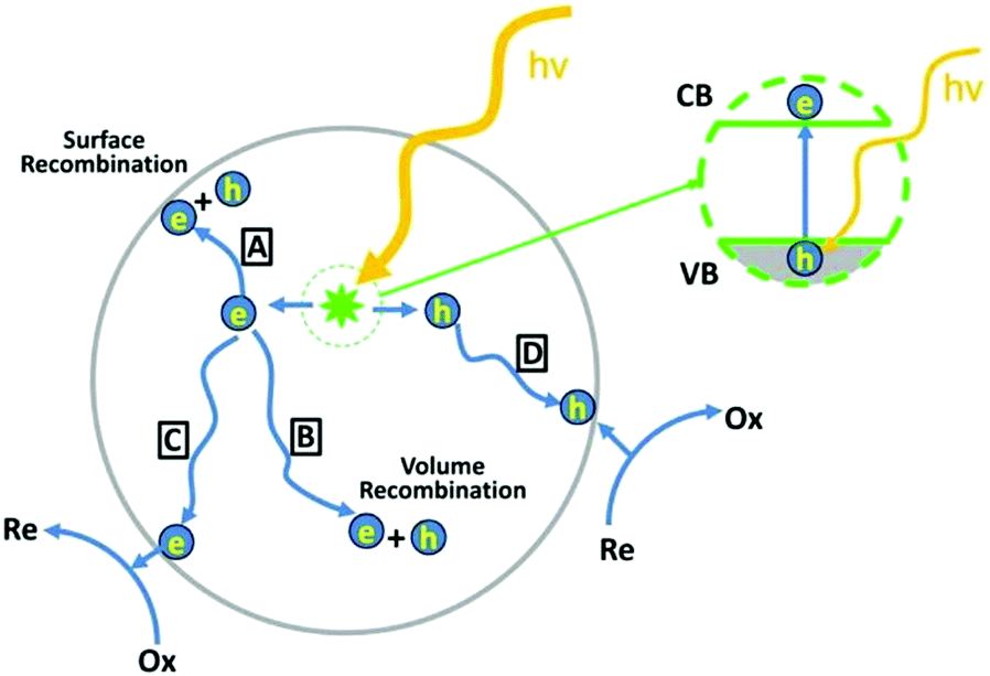 | ||
| Fig. 1 Schematic illustration of the formation of photogenerated charge carriers (electrons (e) and holes (h)) upon absorption of light. Adapted from ref. 25, with permission from the American Chemical Society, 2012. | ||
The properties enumerated previously are mainly dependent on the characteristics of the semiconductor (e.g., energy band structure, free carrier density, presence of defects) and emission spectra of the light source (photon energy).23,26–29 For instance, the photogeneration of electron–hole pairs in the semiconductor is influenced by the width of its band gap and the absorbed photon energy and it may appear in the UV, visible, or infrared (IR) wavelength regime (Fig. 2a). Visible and IR light are more appropriate to activate semiconductors with narrow band gaps (<3 eV) due to their low photonic energy, whereas UV light provides the necessary photonic energy to activate both wide and narrow band gap semiconductors. Hence, common gas-sensitive semiconductors, e.g., TiO2, ZnO, and SnO2 with relatively wide band gaps, usually need higher energy, in the UV range, for their photoactivation (Fig. 2b).
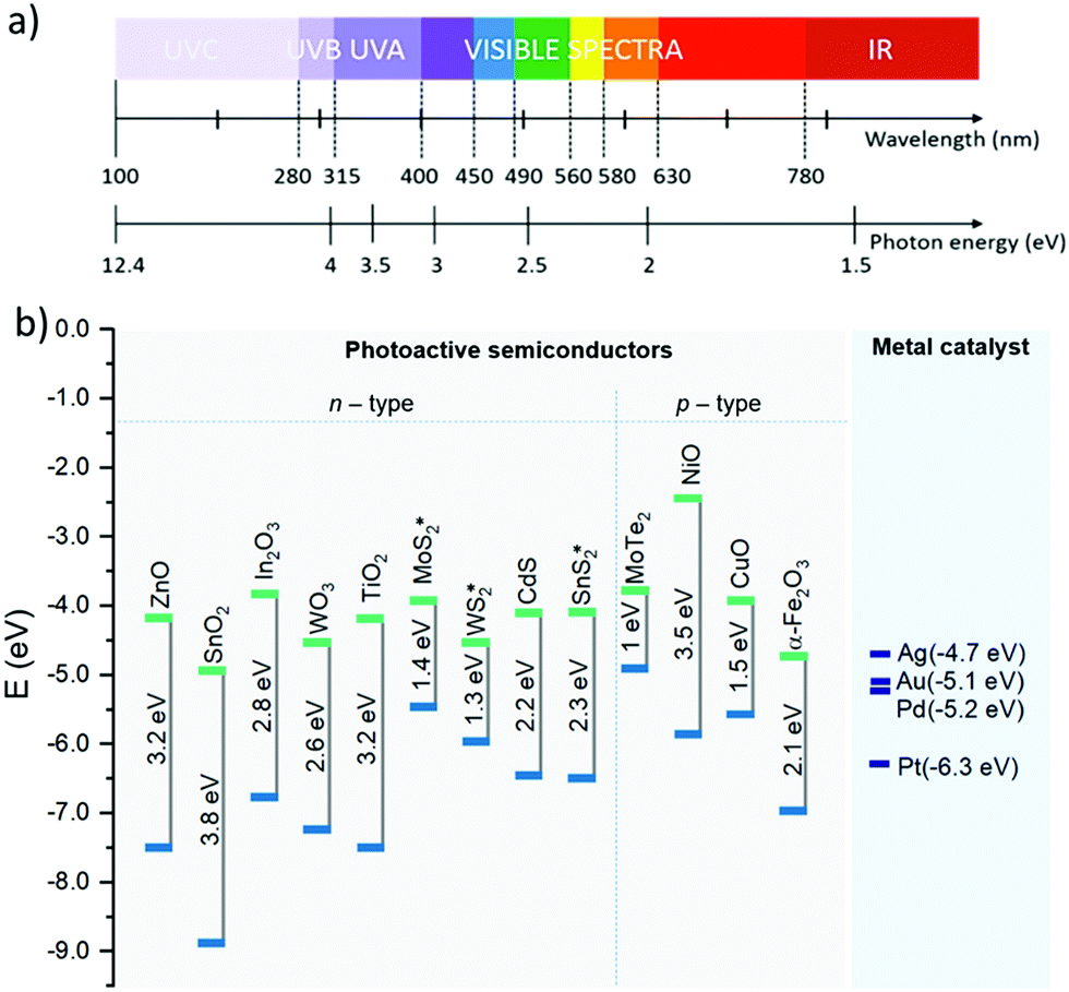 | ||
| Fig. 2 (a) Wavelengths and the corresponding energies for the UV, visible, and IR electromagnetic spectral regimes. (b) Band gaps and band-edge positions with respect to the vacuum level of the most common photoactivated semiconductors used for NO2 sensing. The green and blue lines indicate the lower edge of the conduction band and the upper edge of the valence band, respectively. The data were collected from various reports in the literature;35–39 a star symbol (*) is displayed on the band gaps determined experimentally.40–42 The work functions of various metal catalysts are also displayed on the right side of the figure.43 | ||
The photons exciting the semiconductor with excessive energy (above the threshold of the band gap) can lead to a decrease of the material's chemical activity (e.g., gas sensing properties) due to the dissipation of energy by vibration quanta. Thus, the excitation near the band gap energy of the semiconductor is preferred as it usually provides a maximum in photoactivity and chemical activity.30 Apart from the light wavelength, the irradiance of light is another factor that influences the photoactivation and the gas sensing properties of the semiconductor. The irradiance is not always reported in the gas sensing literature, and instead of it, some authors report the radiant power, also called radiant flux. However, it is important to note that these are different parameters. In radiometry, radiant flux [W] is explained as the radiation power given off from a radiation source per unit of time, while irradiance [W m−2] is defined as the power per unit area of electromagnetic radiation incident on the surface.31 Thus, the irradiance at a particular point depends on the configuration of the light source and the distance of the light source from the target sample.
As far as the rate of transfer of electron–hole pairs and their recombination are concerned, these steps are linked in part to the band bending properties of the semiconductor, i.e., the arrangement of the free charge carrier concentration near the semiconductor surface and the formation of potential energy barriers. In general, the band bending and its orientation depend on factors such as the dopant concentration and the presence of interfaces (e.g., metal–semiconductor and semiconductor–semiconductor junctions), which may have a strong influence on enhancing the electron–hole separation.25 Another critical factor is the crystalline quality of the material, with the crystalline defects acting as centers for electron–hole recombination and scattering of itinerant electrons and holes, which is unfavorable for the diffusion of charge carriers.32
Hence, the tuning of semiconductor properties such as the morphology, structure, surface, doping, and composition is a highly desirable. Material engineering can contribute towards this and realise new optimized semiconductors with both highly efficient photoactivated chemical reactions at the surface and minimum photoexcitation energy, preferentially in the visible wavelength range. The possibility of exciting semiconductors in the visible wavelength range could provide different advantages according to the application. The general rationale behind this preference includes, for instance, in electronics, the efficient use of energy (targeting to consume low or zero electrical power) or, in catalysis, the exploitation of the solar spectrum, which contains a higher percentage of visible light (∼5% UV, ∼43% visible, and ∼52% IR). Another technical aspect includes the wider availability, to date, of light sources in the visible range (e.g., conventional discharge lamps, tubes, and LEDs); light devices with high photonic energy (UV range) are still technologically and materially more expensive than those in the visible range.33
Further details related to strategies and approaches for achieving efficient photoactivation and photochemical reactions on semiconductor surfaces can be found elsewhere.23,25,27,28 In the literature, several review papers discuss the properties and performance of gas-sensitive materials under photoactivation.16,17,34 The following sections of this review focus exclusively on the use of photoactivation for sensing low NO2 concentrations and the most successful materials and interface systems used to this end.
3. Photoactivated sensing for NO2 detection
The photoactivation in semiconductor materials is usually connected with the increased density of electrons in the CB, which in turn promotes the surface activity of the semiconductor. In gas sensing, this is manifested as a direct improvement of the sensing performance, for instance, in sensitivity and response/recovery time, in contrast to non-photoactivated semiconductors operating at room temperature. Below, the possible mechanism and steps involved in the photoactivated response to NO2 are discussed.44–46Initially, when a gas-sensitive semiconductor is exposed to ambient air, without photo- or thermoactivation, oxygen molecules are adsorbed onto the semiconductor's surface. In this step, oxygen captures the electrons from the semiconductor's CB, forming oxygen ions (O2(ads)−), as shown in eqn (1).
| O2(gas) + e− → O2(ads)− | (1) |
| O2(ads)− + hhν+ → O2(gas) | (2) |
| O2(gas) + ehν− → O2(hν)− | (3) |
Subsequently, when the photoactivated sensing material is exposed to NO2, the gas molecules react with the photogenerated oxygen species (eqn (4) and (5)), or even directly with the photogenerated electrons from the CB (eqn (6)). This causes a dramatic change in the electron density of the semiconductor and, in turn, in its conductivity, which is connected with the sensor response and final performance.
| NO2 + O2(hν)− → NO2(hν)− + O2(gas) | (4) |
| 2NO2 + O2(hν)− + ehν− → 2NO3(hν)− | (5) |
| NO2 + ehν− → NO2(hν)− | (6) |
| NO2(hν)− + h+ → NO2(gas) | (7) |
| 2NO3(hν)− + 2h+ → 2NO2(gas) + O2(gas) | (8) |
3.1. Single or non-modified photoactive materials (oxides, dichalcogenides, graphene)
Metal oxides (MOX) such as zinc oxide (ZnO), indium oxide (In2O3), tungsten oxide (WO3), and nickel oxide (NiO) and transition metal dichalcogenides (TMDCs) such as molybdenum ditelluride (MoTe2) are mostly reported in the literature as light-activated bare semiconductors that enable NO2 sensing at sub-ppm concentrations at room temperature. A summary of these materials and their key properties is shown in Table 2.| Material | Morphology | CG | R dry (%) | C (ppb) | R H2O (%) | C/RH (ppb)/(%) | T res/Trec (s)/(s) | λ (nm) | E e (mW cm−2) | Ref. |
|---|---|---|---|---|---|---|---|---|---|---|
| NWs: nanowires; F: films; NDs: nanodisks; L: layer; NPs: nanoparticles; NRs: nanorods; NTs: nanotubes; C/S: core/shell; NS: nanosheets; S: sheets; NCs: nanocubes; C: coatings; NFs: nanofibers; Rdry: response in a dry environment; RH2O: response in a humid environment; CG: carrier gas; C: concentration; Tres: response time; Trec: recovery time; λ: light wavelength; Ee: irradiance; Ref.: references.a The information about irradiance [mW cm−2] is not always included in the reports, or it is substituted with a different parameter, such as radiant energy or radiant power [W] which is not included in the table.b The unit for Ee is cd m−2, N/A: data not available. | ||||||||||
| Single sensing materials | ||||||||||
| ZnO | F | Air | 1310 | 400 | >500 | 400/80 | 19/32 | 365 | 0.6 | 51 |
| 6.6 | 2.5 | |||||||||
| ZnO | NWs | Air | 708 | 1000 | >400 | 1000/80 | 31/144 | 360 | 0.8 | 49 |
| 48 | 20 | |||||||||
| ZnO | F | Air | 240 | 50 | >100 | 50/57 | N/A | 365 | 0.02 | 50 |
| 165 | 25 | |||||||||
| ZnO | F | Air | 180 | 400 | N/A | N/A | 822/N/A | 480 | N/A | 52 |
| In2O3 | NWs | Air | 452 | 500 | N/A | N/A | N/A | 460 | 5.4 | 58 |
| WO3 | F | Air | 190 | 160 | N/A | N/A | 894/1098 | 480 | 0.0004 | 55 |
| NiO | NDs | Air | 31 | 372 | 30 | 372/100 | 792/1746 | 480 | N/A | 59 |
| 12 | 57 | |||||||||
| MoTe2 | L | Air | 18 | 20 | N/A | N/A | 300/120 | 254 | 2.5 | 60 |
| Metal–semiconductor junctions | ||||||||||
| Ag–ZnO | NPs | Air | 180 | 1000 | >180 | 1000/97 | 140/130 | 470 | 75 | 61 |
| 60 | 500 | |||||||||
| Pd–ZnO | NPs–NRs | Air | 160 | 100 | <105 | 100/80 | 25/29 | 475 | 0.8 | 62 |
| 6.6 | 5 | |||||||||
| Au–WS2 | NPs–NTs | Air | 20 | 250 | N/A | N/A | N/A | 530 | N/A | 39 |
| Semiconductor–semiconductor (n–n) junctions | ||||||||||
| ZnO–In2O3 | NPs–NRs | Air | 406 | 500 | 320 | 500/90 | 100/31 | 365 | 5 | 44 |
| 50 | 50 | |||||||||
| CdS–ZnO | C–NWs | Air | 6.7 | 5 | N/A | N/A | 27/53 | 468 | 0.7 | 63 |
| ZnO–SnO2 | NRs–NPs | Air | 150 | 200 | N/A | N/A | 420/480 | 380 | 0.7b | 64 |
| Semiconductor–semiconductor (p–n) junctions | ||||||||||
| MoS2–ZnO | NS–NWs | N2 | 8.4 | 50 | N/A | N/A | 60/60 | 365 | N/A | 40 |
| MoS2–ZnO | NS–NRs | Air | 91 | 5 | N/A | N/A | 132/110 | 365 | 0.3 | 65 |
| Cu2O–ZnO | NCs–NRs | Air | 485 | 100 | N/A | N/A | N/A | N/A | N/A | 66 |
| CuO–ZnO–Cu2O | C | Air | 124 | 200 | N/A | N/A | 756/768 | N/A | 150 | 67 |
| Semiconductor–carbon heterojunctions | ||||||||||
| TiO2–G | NPs–S | Air | N/A | N/A | 17 | 70/40 | 35/90 | 400 | N/A | 68 |
| SnO2–rGO | NFs–NS | Air | 23 | 500 | 15 | 5000/90 | 426/438 | 365 | 97 | 69 |
| SnS2–rGO | S | Air | 13 | 15 | N/A | N/A | <250/<250 | 650 | 1 | 70 |
| Multi-component sensing materials | ||||||||||
| Fe2O3–MWCNTs–WO3 | F | Air | 0.67 | 50 | N/A | N/A | 232/71 | 365 | N/A | 71 |
| Au–Ag–MWCNTs–WO3 | NPs–F | Air | N/A | N/A | 25 | 100/50 | 267/N/A | 365 | N/A | 72 |
| Au–Cu2O–ZnO | NPs–NCs–NRs | Air | 1050 | 100 | N/A | N/A | N/A | N/A | N/A | 66 |
| 26 | 5 | |||||||||
ZnO, on the top of the list, is an n-type semiconductor with a broad direct band gap (3.1–3.3 eV), and optical/electrical properties that are significantly influenced by the presence of defects, e.g., oxygen vacancies (VO), zinc interstitials and zinc vacancies.47,48 Previously, various ZnO structures in the form of nanowires,49 nanofilms,50 and macro/mesoporous51 or porous coatings52 have proved to be appropriate for NO2 sensing under photoactivation. For instance, ZnO nanowires with VO rich surfaces were photoactivated using a UV lamp with a wavelength of 360 nm and an optimal irradiance of 0.8 mW cm−2 to detect NO2. These sensors displayed responses of 48% to 20 ppb of NO2 with response and recovery times of 31 s and 144 s, respectively. Results demonstrated that the response of photoactive ZnO is significantly enhanced, by 2.7 times, compared to VO-deficient ZnO surfaces.49 Similar investigation on the variations of VO concentrations in ZnO showed that the response of rich VO porous coatings with a narrow band gap (2.15 eV) reaches 180% to 400 ppb of NO2 under visible light (λ = 480 nm) excitation;52 though the time required for the response was long (13.7 min). Further studies found that the gas sensing properties of ZnO nanofilms with VO are dependent on not only the amount of VO but also the VO states, such as neutral vacancies (V0O), singly ionized states (V1+O), and double ionized states (V2+O). The greatest responses towards NO2 were recorded on annealed (400 °C) ZnO nanofilms (band gap of 3.13 eV), in which the transition of V0O to V2+O occurred. Li et al. found that the presence of V2+O on ZnO favors the adsorption of NO2 in ambient O2 and enhances the sensor response. The opposite effect was noticed for ZnO with V0O, in which the majority of vacancies were occupied by the adsorbed O2. Eventually, the sensors based on ZnO with V2+O showed a response of 165% to 25 ppb of NO2 under UV light (λ = 365 nm) activation.50 ZnO films composed of hierarchically porous nanorods also showed response (6.6%) to 2.5 ppb of NO2 under UV illumination (λ = 365 nm), with response and recovery times in the range of seconds, 19 s and 32 s, respectively.51 The authors of this work concluded that highly porous ZnO films processed by microwave heating have better sensing performances compared to dense nanorod-based films obtained under conventional heating. This was attributed to the increased amount of macropores and mesopores in the films, which enabled the efficient penetration and scattering of UV light within the film and improved adsorption and diffusion of the NO2 gas.
WO3 is another NO2 sensitive MOX that is considered as a visible-light-driven n-type semiconductor due to its wide band gap energy (2.6–3.2 eV).53,54 Previously, WO3 showed sensitivity to low NO2 concentrations under light activation.55 A study of its performance in the UV to visible light (380–590 nm) range showed a strong dependence of its response on the light wavelength used. An enhancement of the sensitivity and speed of response and recovery times to NO2 was registered by using visible light (λ = 480 nm) and an irradiance of 0.37 W cm−2. For these conditions, the sensors showed a response of 190% to 160 ppb of NO2 with response and recovery times of 14.9 and 18.3 min, respectively.
In2O3 is also an n-type gas-sensitive semiconductor with an indirect band gap in the range of 2.6–2.8 eV.56,57 This semiconducting oxide is considered as a photoactive material with the possibility of absorbing a wide solar spectral range.58 Thus, In2O3 was used previously in the form of parallel aligned nanowires for detecting 500 ppb of NO2 across the full spectrum of visible light (from blue to red) with the highest response (452%) obtained in blue light (λ = 460 nm). Interestingly, this material also showed high response (23%) to 10 ppb of NO2 under polychromatic light sources (white LED). The results were attributed in part to the use of parallel nanowire arrays aligned under deposited interdigital electrodes (ITO). This structure provided a high specific surface area and facilitated electron mobility.
NiO also belongs to the list of photoactive materials for NO2 sensing. This oxide behaves as a p-type semiconductor and has a wide band gap (3.2–4.0 eV).73 Recent studies showed that it shows strong absorption in the whole visible light region and sensitivity to NO2 ppb-levels when black NiO in the presence of Ni3+ ions and VO is used as a sensitive-material.59 Indeed, the large specific surface area and higher porosity of NiO nanodisks showed the greatest sensing properties compared to other nanostructures (nanosized grains and nanosheets) due to the high concentrations of VO and Ni3+ ions. The optimal sensing performances for this material, including a response of 31% to 372 ppb of NO2 and response and recovery times of 13.2 and 29.1 min, respectively, were obtained under blue light illumination (480 nm). The magnitude of the response and the speed of response/recovery for the sensors based on NiO nanodisks decreased for lower wavelengths.
Two-dimensional TMDCs are another class of photoactive semiconductor materials used for NO2 sensing. They are layered materials in the form of MX2, where M is a transition metal (e.g., Mo, W) and X is a chalcogenide (e.g., S, Se, and Te) covalently bonded. TMDCs are intensively studied in various photocatalytic applications (e.g., water splitting, CO2 reduction, gas sensing) due to their narrow band gap and absorption in the wide region of the solar spectrum, as well as high charge carrier mobility. The most common TMDCs, including molybdenum disulphide (MoS2), molybdenum telluride (MoTe2), and tin sulphide (SnS2), have been used as active NO2 sensitive films under light activation in either their single or modified form.17 The examples for single or bare TMDCs used in the literature for detection of NO2 at ppb levels are rare; hence our survey displays only a study of p-type MoTe2 layers in Table 2.60 This material showed a response of 18% to 20 ppb of NO2 and response/recovery times of 5 min/2 min, respectively, under UV illumination with a wavelength of 254 nm and an irradiance of 2.5 mW cm−2. Discussion on other TMDCs forming interfaces, e.g., with metals or oxides, is considered further in the sections dedicated to modified photoactive materials.
The materials exposed above also revealed other functional characteristics (apart from the response, sensitivity, and response/recovery times) of great importance, such as selectivity, humidity interference, and long-term stability. For instance, sensors based on ZnO macro/mesoporous films51 reported good NO2 selectivity over other typical air pollutants such as ethanol (C2H5OH), sulfur dioxide (SO2), hydrogen sulfide (H2S), carbon monoxide (CO), and methane (CH4). Also, a good selectivity to NO2 was noticed for ZnO nanowires49 compared to nitrogen oxide (NO), formaldehyde (HCHO), C2H5OH, CO, and CH4. The evaluation of In2O3 nanowires’ gas selectivity also showed good affinity to NO2 concerning other gases such as H2S, ammonia (NH3), TMA, acetone (C3H6O), benzene (C6H6), C2H5OH, toluene (C7H8), and xylene (C8H10).58 Similarly, systems based on NiO nanodisks indicated good selectivity to NO2 by showing at least four times higher responses to this gas as compared to others (e.g., NH3, HCHO, acetaldehyde (C2H4O), hydrogen (H2)).59 Moreover, humidity tests showed in general that n-type photoactive semiconductors exhibit decreased response to NO2 in a humid environment (see Table 2), while p-type semiconductors such as NiO show the lowest moisture dependence. The stability tests for some of the systems, displayed in Table 2, showed low decreases in the response over 15 days for ZnO porous films52 and after 90 days for ZnO macro/mesoporous films,51 ZnO nanowires,49 and In2O3 nanowires,58 indicating relatively good middle-term stability for these materials.
In summary, ZnO is one of the most representative bare photoactive semiconductors used for sub-ppm NO2 detection under UV illumination. The potential of other semiconductors such as WO3 and In2O3 has also been identified due to their visible-light-driven response towards low NO2 concentrations. Generally, the improvements in the photoactivated gas sensing performance of these materials have been connected to either their specific morphology or structural surface defects such as vacancies. The presence of VO can narrow the band gap width of semiconductors and cause the reduction of the energy required for electron transition. Thus, the structures with a higher VO amount may enable the photoactivation of the semiconductor (e.g., ZnO, NiO) under visible light. Moreover, the presence of VO can improve the charge carrier generation and separation efficiency and provide an increased amount of active sites on the surface, leading to better adsorption of NO2 and enhanced sensing performance.74 The wavelength of light and irradiance are considered critical parameters that strongly influence the sensor response and dynamics of the response. The increase of the irradiance to a certain threshold value enhanced the sensing response,49 whereas the increase of photon energy (light wavelength decrease) showed a contrary effect on the functionality by decreasing the response and the response/recovery time.55,59
Apart from bare semiconducting materials for NO2 detection, the literature shows many other non-bare materials with the potential of improving the photoactive response to gases and in particular to NO2. These include generally modified (composite) materials with ‘extra’ interfaces (e.g., metal–semiconductor or semiconductor–semiconductor junctions) aiming at increasing the light absorption, promoting the separation/migration of charge carriers, and enhancing the surface gas sensitivity. The most common metals and n- and p-type semiconductors employed in these composites are displayed in Fig. 2b. In the following section, we provide a detailed discussion of these systems in the context of NO2 detection at ppb levels. Generally, the modified photoactive materials are divided into two groups: metal–semiconductor and semiconductor–semiconductor junction systems.
3.2. Modified photoactive materials with metal–semiconductor nanojunctions
The intimate contact of a metal and a semiconductor can lead to the formation of either a Schottky barrier or an ohmic contact, according to the relation of the metal (φm) and semiconductor (φs) work functions. The work function defines the minimum energy needed to remove an electron from the Fermi level to the vacuum level. In that context, a metal with a work function higher than that of an n-type semiconductor (i.e., φm > φs) or smaller than that of a p-type semiconductor (i.e., φm < φs) forms a Schottky barrier; the opposite relation between the metal and semiconductor work functions (e.g., when φm < φs for an n-type semiconductor) leads to the formation of an ohmic contact. Therefore, when an n-type semiconductor gets into contact with a metal to form a Schottky barrier, the free electrons from the semiconductor transfer to the metal until their Fermi energy levels equilibrate. Under this condition, the positive charges (holes) are accumulated on the semiconductor side, whereas the negative charges (electrons) accumulate on the metal side. Thus, a space charge region (depletion layer) is created on the side of the semiconductor, where the free electrons near the metal–semiconductor interface are depleted as compared with the bulk. Due to this phenomenon, the deformation of the band structure or the upward band bending occurs, causing the formation of a Schottky barrier and the presence of an internal electric field from the semiconductor to the metal. For p-type semiconductors, the electrons from the metal are transferred to the semiconductor side, and the space charge region is formed with the downward band bending; the direction of the internal electric field is from the metal to the semiconductor. In the case of ohmic contacts, the depletion layer in the semiconductor is absent (instead, an accumulation layer charge is formed) so that the bands bend in the opposite direction compared to the Schottky junctions.The band bending has been demonstrated to be a complex and fundamental step in light-driven chemical processes. It can significantly decrease the recombination of electron–hole pairs and promote their separation and migration to the semiconductor surface,25,75 so that the photogenerated charge carrier pairs in the metal–semiconductor system can be effectively separated driven by the internal electric fields. The photoexcited electrons can be trapped by the metal particles, while the photoexcited holes enrich the semiconductor side (for an n-type semiconductor). This is the main reason for the enhancement of photoactivity in metal–semiconductor junctions and the promotion of surface reactions.76,77 An improved surface activity can also be connected with these systems due to the catalytic properties of the metal. The presence of metal plays a key role in the activation of surface reactive sites of the semiconductor and the reduction of the activation energy for surface chemical reactions.78,79
In metal–n-type semiconductor materials with Schottky barriers under UV activation (Fig. 3a), the photogenerated electrons with enough energy in the CB of the semiconductor can migrate to the metal overcoming the potential barriers; the separation efficiency is determined by the barrier height (φSB). The electron–hole separation is promoted in the smaller height potential barriers as the photogenerated electrons need less energy to overcome the barrier and migrate from the semiconductor's CB to the metal.80 However, in the case of ohmic contact, the transfer of charge carriers is smoother, as there is no barrier at the metal–semiconductor interface. Incorporating plasmonic metals (e.g., gold nanoparticles) rather than non-plasmonic metals in these systems offers the possibility of extending the light absorption from the UV to the visible region thanks to the surface plasmon effects of these metals when taken to the nanoscale. Therefore, under visible light activation (Fig. 3b), high-energy hot electrons are created in the plasmonic nanoparticles and injected into the CB of the semiconductor whenever the kinetic energy of the electrons is greater than the potential barrier (φSB) between the metal and the n-type semiconductor. The appropriate height of the Schottky barriers prevents the backward flow of hot injected electrons from the semiconductor's CB to the metal, and it contributes to the efficient electron–hole separation and surface chemical reactions. The backward flow of hot electrons is feasible for ohmic contact due to the absence of a barrier, so the electron–hole separation cannot be promoted. Therefore, the tuning of the potential barrier height plays a key role in the photoactivation of plasmonic metal–semiconductor systems (it should not be too high or too small to enable hot electron injection into the semiconductor and avoid the back-flow of hot electrons).81–83Fig. 3 depicts a schematic view of the metal–n-type semiconductor system with Schottky junctions and their photoactivation for both cases discussed above. The electrons from the semiconductor's CB migrate to the metal under UV light, and the photogenerated electrons from plasmonic metal nanoparticles are injected into the semiconductor's CB under visible light.
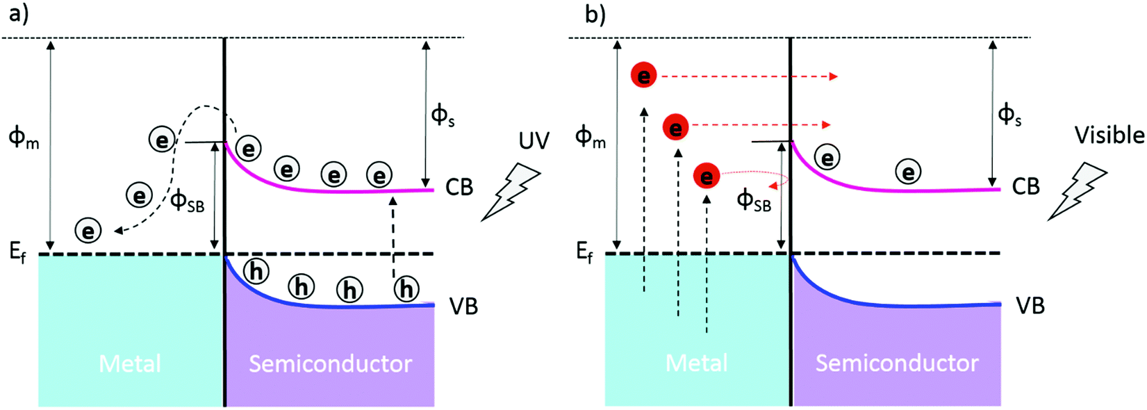 | ||
| Fig. 3 Schematic diagram of a metal–semiconductor system under UV activation showing the photogenerated electrons in the semiconductor with higher energy than the potential barrier (φSB) migrating to the metal (a). Schematic diagram of a plasmonic metal–semiconductor system under visible light activation. (b) Hot electrons in plasmonic metal nanoparticles are excited above the Fermi energy under visible light illumination and these electrons with energies high enough to overcome the φSB can be injected into the CB of the neighboring semiconductor. The diagrams illustrate a metal–n-type semiconductor and a Schottky-type junction. | ||
The field of photoactivated gas sensors usually refers to metal–semiconductor junction-based materials containing noble metals such as gold (Au), silver (Ag), platinum (Pt), and palladium (Pd) and semiconductors such as MOX and TMDCs.17 The systems tested for low NO2 concentrations focus on ZnO and its modification with metals such as Ag61 and Pd,62 as well as WS2 modified with Au39 (Table 2). Overall, these systems showed a response to NO2 under visible light activation. Accordingly, the incorporation of Ag nanoparticles on ZnO enhanced light absorption in the visible range concerning optically inactive bare ZnO nanoparticles thanks to the surface plasmon resonance effect of Ag.61 Thus, Ag-modified ZnO nanoparticles (AgNO3/Zn(NO3)2 molar ratio 3:97) showed a 60% response to 500 ppb of NO2 under visible light activation (λ = 470 nm) with an irradiance of 75 mW cm−2. The sensors exhibited response and recovery times of more than 140 s and 130 s, respectively.61 The authors found, however, that the excessive concentration of Ag (AgNO3/Zn(NO3)2 molar ratios 5:95 and 8:92) influenced the sensor response negatively by reducing the photo quantum efficiency due to the participation of the Ag particles as charge carrier recombination centers. The decrease in the photoactivated surface reactions of highly metal-loaded semiconductors was also described earlier, and the effect was attributed to the increased number of negative metal sites, which could attract and recombine positive holes, lowering the photoactivity at the end.84 Plasmonic-active Au nanoparticles were also used as the source of hot electron generation for the visible light activation of ZnO nanostructures in the form of nanowires85 and nanorods,86,87 although the functionality of these structures was not assessed for NO2 concentrations below 1 ppm.
The modification of ZnO with Pd nanoparticles also influenced the behavior of ZnO, making it optically active in the visible light region and responsive to NO2 due to the injection of photoexcited non-plasmonic electrons from Pd nanoparticles to ZnO.62 The photocatalytic properties of Pd nanostructures under visible light were also investigated previously in the area of photoactivation.76,88 The Pd-nanoparticle modified ZnO rods displayed responses of 160% to 100 ppb of NO2, revealing response and recovery times of 25 s and 29 s, respectively.62 This performance was accomplished under the optimal conditions of visible light (λ = 475 nm) illumination and an irradiance of 0.8 mW cm−2. The enhancement in NO2 response from 85% to 160% was noticed with the increment of the irradiance from 0.3 to 0.8 mW cm−2, respectively. The interference from humidity decreased the response of the Pd–ZnO sensors, and the stability tests showed that a slight decrease in the response occurred during the testing period of 90 days.
Tungsten disulfide (WS2) modified with Au nanoparticles is another material that has shown responsiveness to low NO2 concentrations. The sensing properties of WS2 nanotubes containing Au nanoparticles (HAuCl4/WS2 molar ratio 1:2) were tested under green light illumination (λ = 530 nm).39 Bare and Au modified WS2 sensors showed responses to 250 ppb of NO2. The adsorption of NO2 molecules onto the bare WS2 nanotubes is feasible due to the generation and separation of electron–hole pairs. This occurs as the wavelength energy of the green light exceeds both the indirect (1.3–1.4 eV) and direct (2.0–2.1) band gaps of WS2. The modification of WS2 with Au NPs allowed for sensors with higher sensitivity to NO2 compared to bare WS2 due to the photoactivation of both the Au NPs (i.e., excitation of Au surface plasmon resonance) and the WS2 structures. Overall, the results showed an increase of 10% in the response to 250 ppb of NO2 for the Au–WS2 composite structures compared to the bare WS2 structures.
Further tests of materials mentioned above indicated good selectivity to NO2 (1 ppm) over other pollutants, including NO (1 ppm), C2H5OH (10 ppm), HCHO (10 ppm), NH3 (10 ppm), H2 (100 ppm), and CO (100 ppm) for Pd–ZnO62 junction-based materials. A higher selectivity to 1 ppm of NO2 was achieved though for Ag–ZnO sensors, which showed negligible response to several common interfering gases, including HCHO (25 ppm), CH4 (50 ppm), CO (50 ppm), NH3 (50 ppm), SO2 (100 ppm) and carbon dioxide (CO2) (10000 ppm).61
In summary, the detection of NO2 in the ppb concentration range was only achieved in a few reports, in which either MOX (ZnO) or TMDCs (WS2) were combined with plasmonic (e.g., Au, Ag) or non-plasmonic (e.g., Pd) transition metal nanoparticles. The composite materials reached the photoactivation stage under visible light illumination thanks to plasmonic or even non-plasmonic (as Pd) electron generation in the metals and the sufficient electron–hole separation (with electron transfer into the CB of the semiconductor). The size and shape of the metals modifying the semiconductor, as well as their geometry and the locations to the neighboring semiconductor material, are also critical parameters that affect the efficiency of generation of electron–hole pairs, their separation, and finally, the gas sensing properties.83 However, the correlation of these factors with the sensor performances is absent in literature reports.
3.3. Photoactive materials with semiconductor–semiconductor nanojunctions
This section discusses the properties and processes in photoactive materials containing heterojunctions formed by assembling two or more semiconducting materials. As exposed above, the presence of interfaces formed by the addition of a second semiconductor in the system is an effective way to improve the photoactivation efficiency and enhance the surface reactions. The semiconductor–semiconductor junctions, also known as heterojunctions, are classified either by the type of semiconductor (n or p), or by the alignment of the energy bands of each constituent. Therefore, when it comes to the type of semiconductor, the heterojunctions between two n-type semiconductors or two p-type semiconductors are known as n–n or p–p heterojunction, respectively, whereas the heterojunctions combining both p-type and n-type semiconductors are referred to as p–n heterojunctions. In contrast, when using the band alignment as a reference, three heterojunction types are identified: Type I (straddling gap), Type II (staggered gap), and Type III (broken gap) (see Fig. 4). In this classification, the transfer of electrons and holes through the heterojunctions is believed to occur to the semiconductor that has the CB and VB at the lowest and highest energy levels, respectively.89,90 In Type I alignment, the photogenerated electrons and holes accumulate on semiconductor B as its CB and VB are located within the band gap of semiconductor A. In Type II alignment, the migration of photoexcited electrons occurs from semiconductor A (higher CB level) to semiconductor B (lower CB level), while holes accumulate in the VB with a higher energy level (semiconductor A). A Z-scheme photocatalytic system is also possible in Type II alignment. In this scheme, the photogenerated electrons from the CB of semiconductor B and holes from the VB of semiconductor A recombine, while holes with a strong oxidation ability and electrons with a strong reduction ability are preserved in the VB of B and the CB of A, respectively. The Z-scheme photocatalytic system provides charge separation efficiency and a strong redox ability for driving photocatalytic reactions.91 In Type III alignment, there is no expected migration of photogenerated electron–hole pairs between the two semiconductors due to the broken band alignment.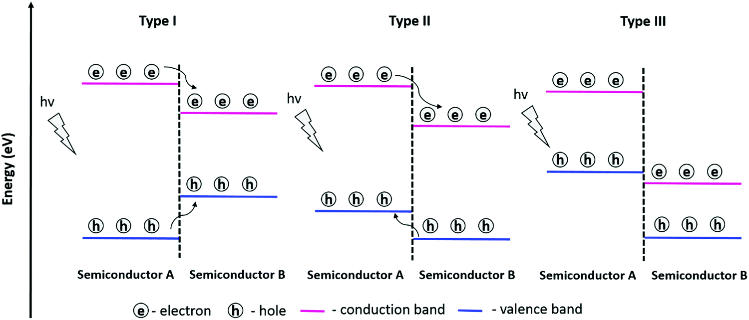 | ||
| Fig. 4 Schematic diagrams of Type I, Type II, and Type III heterojunctions. | ||
The type of band alignment has an influence on the separation of photogenerated charge carriers. In this context, heterojunctions with Type II alignment may be advantageous as the electrons and holes are separated in two semiconductors as opposed to Type I where charge carriers gather in the same semiconductor and have a higher probability of recombination.90,92 Apart from band alignment, the internal electric field across the interface of the semiconductors due to the band bending (effect of the Fermi level equilibrium) also influences the electron–hole separation. The formation of a space charge region is favored in the p–n junction due to the diffusion of electrons from the n-type semiconductor to the p-type semiconductor, and vice versa for the holes. Thus, the built-in electric field at the interface favors the transport of a type of charge carrier (e.g., electron) forbidding the other (e.g., hole) in a specific direction; this contributes positively to the charge separation process and the lifetime of the photogenerated charge carriers.77,93,94 Hence, the design of specific band alignments at the semiconductor–semiconductor junction can improve the photogenerated electron–hole separation and influence directly the surface reactions.94,95
As noticed in Table 2, semiconductor–semiconductor junction-based materials have been reported considerably more than other systems (bare materials or metal–semiconductor junction-based materials) for the photoactive detection of low NO2 concentrations. For instance, n–n type heterojunction systems were formed by combining ZnO with In2O3,44 ZnO with cadmium sulfide (CdS),63 and ZnO with tin oxide (SnO2).64 The band alignment of these composites corresponds to Type II. Hence, in the ZnO–In2O3 heterojunction, with the In2O3 CB above that of ZnO, the photogenerated electrons are transferred from the CB of In2O3 to that of ZnO, while the photogenerated holes are transferred in the opposite direction (i.e., from the VB of ZnO to that of In2O3). This transfer of electrons and holes in opposite directions promotes the separation of photogenerated charge carriers and increases the number of active species that participated in the oxidation or reduction reactions at the surface. Indeed, this model structure (ZnO–In2O3 with 10 mol% In2O3 in ZnO) reported in the literature44 exhibited response (50%) to a low (50 ppb) NO2 concentration with response and recovery times of 100 s and 31 s, respectively, under UV light (λ = 368 nm) activation and an irradiance of 5 mW cm−2. The authors in this work also discussed the influence of In2O3 loading (5, 10, and 15 mol%) on ZnO, showing a compromise in the loaded amounts. Results showed that too low or too high amounts did not represent an improvement for the separation efficiency of charge carriers because either they are not enough to show a change in properties or they incorporate recombination centers. The change in photoactivation efficiency as a function of the concentration of active materials was also observed before.61 The CdS–ZnO composite represents another Type II heterojunction addressed to efficiently separate photogenerated charge carriers and improve the photocurrent of the film. In this system, the electrons from the CB of CdS are injected into the CB of ZnO, while the holes accumulate in the VB of CdS. This composite (i.e. CdS–ZnO core/shell nanowires) achieved the detection of 5 ppb of NO2 under light illumination (λ = 468 nm) and an optimum irradiance of 0.68 mW cm−2. The response (6.7% for 5 ppb of NO2) exhibited good dynamics with response and recovery times of 27 s and 53 s, respectively. Thanks to this structure, which provides a high density of electrons in the CB of ZnO, the response to low concentrations of NO2 is achieved.63 Similarly, the system composed of ZnO and SnO2 suggests a Type II heterojunction, in which the photogenerated electrons are transferred to the CB of SnO2 and the holes accumulate in the VB of ZnO. On testing, this composite, with a Zn/Sn molar ratio of 1:1, displayed response to a low NO2 concentration (200 ppb) using a wavelength light of 380 nm and an irradiance of 0.7 cd m−2 (reported for Rgas/Rair = 2.5, calculated for ((Rgas − Rair)/Rair) × 100 = 150%), although with relatively slow response and recovery times, 420 s and 480 s, respectively.64 The authors of this work also reported a remarkable increase of the photoactivated response with the increase of NO2 concentration to 500 ppb (reported for (Rgas − Rair)/Rair = 1266, calculated for ((Rgas − Rair)/Rair) × 100 = 126600%). However, it is worth noting that this value deviates considerably from others reported in the literature for the same concentrations, as noticed in Table 2.
In the literature, there are also p–n heterojunction systems that have shown successful responses to low NO2 concentrations. Among these, heterojunctions formed by combining ZnO with MoS2,40,65 ZnO with copper(I) oxide (Cu2O),66 and ZnO with a copper(II) oxide (CuO) and Cu2O mixture.67 Different morphologies of ZnO (n-type) in the form of nanowires40 and nanorods65 were mixed with few-layer MoS2 nanosheets (p-type). These systems formed Type II p–n heterojunctions, which suggest that after the photoactivation, efficient separation of the charge carriers is achieved. In the MoS2–ZnO system, the electrons from the CB of MoS2 can move into the CB of ZnO, while holes are transferred from the VB of ZnO into the VB of MoS2, driven by the built-in field at the interface. Thanks to this structure, the sensors based on ZnO nanowires with MoS2 showed a response of 8.4% to 50 ppb of NO2 under UV light (λ = 365 nm) with response and recovery times of about 1 min. Unlike other reports, these results were obtained using nitrogen as the carrier gas for the tests. In addition, this system manifested good selectivity to NO2 compared with several interfering gases (e.g., NO, NH3, H2S, HCOH, CO, H2) and showed long-term stability over three weeks with a gradual response decay. Similarly, the systems formed with ZnO nanorods and MoS2 nanosheets65 showed a good response (91%) to 5 ppb of NO2 using UV activation (λ = 365 nm, irradiance = 0.3 mW cm−2) with response and recovery times of 132 s and 100 s, respectively. The improved performances of these sensors were attributed to the formation of a p–n heterojunction and the presence of abundant adsorption sites, including VO at the ZnO structure and sulfur vacancies and edge defects at MoS2.
The p–n junction can also be established by mixing ZnO (n-type) with CuO and Cu2O (both p-type) as shown in previous work.67 In this heterojunction system, which can be identified as Type II, an internal electric field is created due to the Fermi level alignment so that the electrons from the CB of CuO and Cu2O migrate to the CB of ZnO, while holes move to the VB of CuO and/or Cu2O. The gas sensing test of this composite with highly concentrated donor defects was performed using white light and an irradiance of 0.15 W cm−2. Results showed a response of 124% to 200 ppb of NO2 with relatively long response and recovery times, 12.6 and 12.8 min, respectively. This system also revealed good selectivity to NO2 among other gases such as SO2, C3H6O, C2H5OH, and methanol (CH3OH). The use of p–n junctions based on ZnO nanorods and Cu2O nanocubes was also reported previously for NO2 detection at low concentrations. This composite showed a response of 485% to 100 ppb of NO2.66 Lu et al. stated further improvements to NO2 by adding Au to the Cu2O–ZnO heterojunction system. Thus, the addition of Au led to a response of 1050% to 100 ppb of NO2.
In the literature, one can also find composites containing traditional materials (e.g., MOX, TMDCs) and other new materials with semiconducting properties based on carbon (e.g., graphene, reduced graphene oxide (rGO)) that have been used for the photoactivated detection of NO2. For instance, the rGO–SnO2 composite, identified as a p–n type heterojunction, exhibited a sensing response of 23% to 500 ppb of NO2 with good selectivity over other analytes (SO2, NH3, HCOH, H2, CH4, and C8H10)69 by using UV light activation (λ = 365 nm, irradiance = 97mW cm−2). In this system, the electron–hole pairs are photogenerated in SnO2 and electrons migrate to rGO driven by the built-in electric field. Humidity tests of the rGO–SnO2 sensor to 11% to 89% RH showed its stable sensing ability in this range, although with a decrease of the response to 5 ppm of NO2.
Another example of p–n heterojunctions is represented by rGO (p-type) and SnS2 (n-type) semiconductors.70 This system with different contents of rGO in the mixture was found to have a direct influence on the gas sensing response of rGO–SnS2 composites under light illumination. Generally, samples with low rGO loads in the SnS2–rGO mixture (i.e., predominantly n-type behavior) enhanced the visible light-activated response (λ = 650 nm, irradiance of 1 mW cm−2) to NO2 by a factor of approximately six compared to non-photoactivated samples. On the other hand, samples with high rGO loads in the SnS2–rGO mixture (i.e., predominantly p-type behavior) showed negligible differences in response to NO2 with and without visible light activation. The results for the n-type SnS2–rGO mixture were attributed to the significant differences between the work functions of each material, which allowed a large number of electrons to be transferred from the rGO to the SnS2. Even though this should also be valid for the p-type SnS2–rGO mixture, the fact that a poor photoelectric material, for example rGO, is dominant in the sample makes the whole SnS2–rGO mixture poorly photoactive. Graphene sheets containing embedded TiO2 nanoparticles were also investigated as a photoactive material for NO2 sensing. Comparative tests of their response to 1750 ppb of NO2 with and without photoactivation indicated two-fold higher responses by the photoactivation of the material. Further photoactivated tests (λ = 400 nm) showed a response of 17% to low NO2 concentrations (70 ppb) in a humid environment (40% RH).68
The mixture of more than two types of materials based on Fe2O3–MWCNTs–WO3 for the photoactivated response to NO2 was also reported in the past,71 although without a specific mention of the formation and influence of junctions in the sensing properties of the composite films. Laboratory tests of these composite films showed a response of 0.67% to 50 ppb of NO2 under pulsed UV illumination (365 nm) and response and recovery times of 232 s and 71 s, respectively. The selectivity tests indicated a remarkable response to NO2 compared to other gases (NH3, SO2, CO, and H2S). Further tests of these sensors in the exhaust of a motorcycle in the idling position proved their on-field applicability by detecting NO2 (∼232 ppb).71 The combination of p–n heterojunctions and metal-semiconductor junctions in the same systems was also tested previously by using ZnO–Cu2O composite films modified with Au.66 Lu et al. claimed that the addition of Au to the mentioned system provides further efficiency to the separation of photogenerated electron–hole pairs. Therefore, the response of Au–Cu2O–ZnO based sensors (1050%) doubles the response of ZnO–Cu2O (485%) to 100 ppb of NO2, when using continuous UV illumination (irradiance not available in the report).
In summary, photoactivated gas-sensitive materials with both n–n and p–n type heterojunctions were used for detecting sub-ppm NO2 concentrations. Most of the combinations that involve n- and p-type semiconductors correspond to Type II band alignment, which is known to provide better separation of photogenerated electron–hole pairs. We observed that among n-type semiconductors, ZnO is one of the most common materials in these combinations, while MoS2, CuO, and Cu2O attracted more attention from the group of p-type materials. Most of the sensors based on semiconductor–semiconductor junctions exhibited NO2 response under UV activation (365 or 380 nm), while only CdS–ZnO and SnS2–rGO showed response in the visible range of light (468 nm and 650 nm, respectively). The last systems, which contain narrow band gap semiconductors (e.g., CdS (∼2.4 eV),35 SnS2 (∼2.3 eV)42), can have a strong absorption potential in the visible region, ensuring the photoactivation of the composite material (narrow/wide band gap semiconductors)26 and the response to NO2 under visible-light illumination.
3.4. Organo-functionalized hybrid nanomaterials
Chemical sensors based on photoactive metal oxides (e.g., WO3, SnO2, ZnO, In2O3), metal sulfides (e.g., CdS, MoS2 and SnS2), and carbon (SWCNTs, graphene, rGO) have shown responses to NO2, as well as other gases, proving relatively fast response and sensitivity to sub-ppm NO2 concentrations.59,60,96,97 Previous sections showed that these characteristics can be improved further by forming nanoscale interfaces within the materials, with either metal or semiconductor modifiers. Although less discussed in the literature, another possible surface modification path for improving the photoactivity of gas-sensitive materials involves the use of organo-functional groups. Indeed, this has been used previously as an alternative to enhance the properties of bare and modified sensitive materials98 both under thermoactivation98–100 or at room temperature101,102 and also recently by applying photoactivation.103,104 The variety of organic functionalities offers a broad spectrum of combinations for new sensing photoactive hybrid materials. The role of these organic molecules is to modify the surface structurally and in terms of chemical nature to create more active sites enhancing the gas sensing behavior.100Table 3 displays selected examples of these types of modified nanomaterials for NO2 sensing.| Material | Synthesis | Morphology | C (ppm) | R dry (%) | T (°C) | λ (nm) | Ref. |
|---|---|---|---|---|---|---|---|
| C: concentration; Rdry: response in a dry environment; T: temperature; λ: wavelength; Ref.: references; APTES: 3-triethoxysilylpropylamine; AACVD: aerosol assisted chemical vapor deposition; RT: room temperature; DNA: deoxyribonucleic acid; CTMA: cetyltrimethylammonium chloride; DBSA: dodecylbenzenesulfonic acid; PPy: polypyrrole; en-APTAS: N-[3-(trimethoxysilyl)-propyl]-ethylenediamine; CSA: camphorsulfonic acid. | |||||||
| Phototactivated | |||||||
| APTES/WO3−x | Silanization/AACVD | Nanowires | 10 | 5.5 | RT | 356 | 103 |
| DNA-CTMA functionalized GaN | Plasma-assisted molecular beam epitaxy | Thin films | 100 | 19 | RT | 364, 254 | 104 |
| Non-photoactivated | |||||||
| Polythiophene/WO3 | Colloidal chemical method | Nanocrystalline powder | 100 | 1200 | 70 | — | 99 |
| APTES/WO3 | Polymer electrospinning – annealing | Porous nanotubes | 1 | 4400 | 340 | — | 100 |
| Titanyl phthalocyanine/ZnO | Vapor phase growth technique | Tetrapod-shaped nanocrystals | 0.5 | 145 | 25 | — | 98 |
| DBSA doped PPy–WO3 | Mechanical mixing method/drop casting | Nanoparticles | 100/5 | 72/12 | RT | — | 101 |
| en-APTAS/SnO2 | Self-assembled monolayer | Layers/nanowires | 0.4 | 2100 | RT | 450, 650 only for desorption | 102 |
| CSA/PPy–ZnO | Polymerization/sol–gel/spin-coating | Aggregation of nanoparticles | 100 | 80 | RT | — | 105 |
| PPy/Fe2O3 | Hydrothermal process | Microspheres/nanoparticles | 0.1 | 220.7 | 50 | — | 106 |
Recently, for instance, WO3−x nanowires modified with (3-aminopropyl)triethoxysilane (APTES) molecules by silanization showed UV light-activated response to NO2 and ethanol at room temperature.103 Tests of these organo-functionalized structures showed their nearly eight times higher sensitivity (ppm−1) to NO2 and improved response dynamics, as compared to bare WO3−x nanowires, with further improvements (about four-fold the sensitivity of APTES@WO3−x) by using APTES modified CeO2–WO3−x structures. These results were attributed in part to the presence of the reactive amino group of APTES at the surfaces of WO3−x and CeO2–WO3−x, which favors the reactivity towards polar gaseous molecules. Results were also connected with the UV light activation, which allows the transfer of electrons from the APTES to the metal oxide conduction band, increasing its conductivity and facilitating the reaction with the gases. Along a similar line, the UV light activation of bare gallium nitride (GaN) films functionalized with deoxyribonucleic acid (DNA) in complex with cetyltrimethylammonium chloride (CTMA) proved to be sensitive to NO2 at room temperature.104 This study proposed that the functional groups in the DNA–CTMA compounds (–NH3, OH) are responsible for the increase of the surface charge density at GaN so that the charge transfer between GaN and NO2 gas molecules is likely increased. The tests showed that the modified GaN (DGaN) has a better response (37.33%) to NO2 under 254 nm UV illumination than without UV illumination (19%). The authors inferred that the charge carriers are generated on the surface of the material under UV light activation, and this further can enhance the ionization of pre-adsorbed O2 molecules. These aspects led to a significant increment of active species at the material surface, improving the response of the DGaN sensors to NO2 under UV light activation.
As noted in Table 3, the list of light-activated hybrid materials for NO2 sensing in the literature is short. However, one can find examples of other hybrid materials that have been used for NO2 detection (at room temperature or under thermoactivation), and that might be improved by using light-activated sensing. For example, polythiophene (PTP) was used for the functionalization of nanocrystalline WO3 powder by an in situ chemical oxidative polymerization method. This electron donor–acceptor system, composed of PTP molecules and WO3 particles that behave as p- and n-type semiconductors, respectively, was employed to increment further the depletion barrier height of the bare WO3 particles and improve the response of the sensor to NO2. Tests to 100 ppm of NO2 corroborated the improvement showing a response of 110% for bare WO3 and 1200% for PTP–WO3 at 70 °C.99 Similarly, WO3 porous nanotubes functionalized with APTES molecules showed sensitivity to low NO2 concentrations, though using thermal activation at 340 °C.100 Tests to 1 ppm of NO2 demonstrated that the introduction of APTES increases the response of pristine WO3 from 90% to 4400%, respectively. The authors also found that the concentration dependence of response has a linear behavior with a measured detection limit of 10 ppb (response = 25%). The results were attributed to the incorporation of amino groups (due to the APTES molecules) that exhibit strong electron-donor properties and tend to form hydrogen bonds with the unpaired electrons of the oxygen from the NO2 gas. Another hybrid material based on SnO2 nanowires functionalized with N-[3(trimethoxysilyl)propyl]ethylenediamine (en-APTAS) also showed a non-photoactivated response to NO2 at room temperature (<28 °C); however, it proved the need for visible light illumination (450 and 650 nm) to enhance and accelerate the gas desorption process.102 The results of this system towards several gases, including SO2, CO, CO2, NH3, NO, and NO2, reported the major response (2100%) to NO2 at a sub-ppm concentration (400 ppb).
Titanyl phthalocyanine (TiOPc) functionalized ZnO nanotetrapods were also used for detecting NO2 without photoactivation.98 In this system, the organic molecule modified the sensitivity of the nanostructure at low temperatures (i.e., room temperature), obtaining a good response (14500%) for 500 ppb of NO2, although with slow dynamics since the time to reach this response needed more than 60 min. This strong sensitivity was connected with the formation of localized p–n heterojunctions at the surface of n-type ZnO and p-type TiOPc and the possibility of exchanging charge carriers at this hybrid–composite interface. Another example of hybrid NO2 sensitive materials working at room temperature also includes dodecylbenzenesulfonic acid (DBSA) doped polypyrrole–tungsten oxide (PPy–WO3) nanocomposites, which showed high sensitivity to NO2 gas with 72% and 12% response to 100 ppm and 5 ppm, respectively.101 The authors of this work proposed the formation of p–n junctions distributed at the surface of this material and electron charge transfer mainly between NO2 and PPy, with the role of DBSA centered in enhancing the rate of reaction by creating additional active sites in the PPy–WO3 hybrid nanocomposite. Previously, a hybrid sensor of polypyrrole–zinc oxide (PPy–ZnO) doped with camphorsulfonic acid (CSA) was also evaluated for NO2 sensing at room temperature, obtaining 80% of the response to 100 ppm of NO2.105 In summary, organo-functionalized hybrid nanomaterials have proven to be alternatives for the photoactivated detection of not only NO2, but also other gases/vapors reported previously, e.g., acetone, nitromethane, triethylamine,107 methanol,108 ammonia,109 and hydrogen sulfide.110
4. Key enabling technologies
4.1. Synthetic procedures (MOX, dichalcogenides, composites)
The literature shows a variety of nanomaterials with attractive features for the photoactivated detection of NO2 at room temperature. These usually include metal oxides (ZnO,51,111 In2O3,58,96,112 WO397), metal sulfides (SnS2,113 MoS2114), carbon nanostructures (SWCNTs,115 graphene,116 rGO117), and surface-modified or nanostructured composites (e.g., ZnO–Pd,62 MoS2–Au,118 SnS2–rGO,70 ZnO–rGO,119 CuxO1−y–ZnO2−α67). The last usually provide enhanced performance compared to bare materials, as stated in the sections above. The properties of these materials are strongly influenced by their crystalline size, dimensions, and morphology,120 and therefore their controlled synthesis plays an important role in their final performance and functionality.Generally, the decrease of NP size enhances the efficiency of photocatalyst materials since the proportion of available surface area increases while maintaining the intrinsic activity of the material. However, it must be noted that this has an increasing effect on the quantum confinement, which enlarges the optical energy band gap of the material, and so, size reduction may sometimes reduce photo-efficiency (Fig. 5a), as determined previously for ZnO120 and anatase TiO2.121
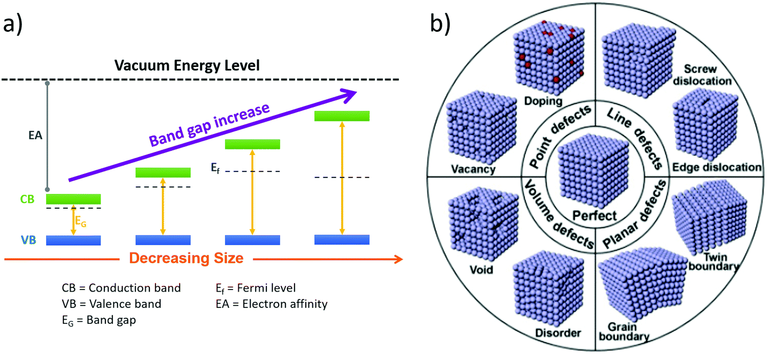 | ||
| Fig. 5 (a) Energy band variation in nanoparticles as the size decreases to the quantum dot classification (adapted from ref. 130, with permission from AIP Publishing, 2020). (b) Schematic illustration of crystal defects with different atomic arrangements in photocatalytic materials (adapted from ref. 124, with permission from Elsevier, 2018). | ||
The crystalline quality of the material also influences the light–solid interactions, i.e., photon absorption, charge-carrier formation, dynamics, and surface trapping. Crystal defects have generally negative effects on the photocatalytic properties since defects act as centers for electron–hole recombination and scattering of itinerant electrons and holes, which is unfavorable for the diffusion of charge carriers. However, in specific cases, the defect-controlled synthesis of photocatalytic materials may be strategic to improve properties such as the band structure of semiconductors to extend the light absorption range122 and/or add active sites for catalytic reactions.123,124 A schematic illustration of the possible defects in crystalline materials is displayed in Fig. 5b. Usually, defects are divided into four groups: point defects (e.g., vacancy and doping), line defects (e.g., screw dislocation and edge dislocation), planar defects (e.g., grain boundary and twin boundary), and volume defects (e.g., lattice disorder and void).124,125
The literature shows numerous synthetic methods to achieve a controlled synthesis of materials with photosensitivity to NO2,58,62,67,113,114,118,119,126–128 as noticed in Table 4. However, against a host of competing synthetic methods, those considered as bottom-up methods are a recurrent strategy for the synthesis of bare and composite materials, probably because these methods are generally more affordable and enable the tuning of key parameters such as the size (nano/micrometer range), shape (thin films, nanorods, nanosheets, etc.), and crystallinity of the material in a fairly reproducible manner.129
| Method | Material | Type of SC | Morphology | Dimensions (nm) | Ref. |
|---|---|---|---|---|---|
| SC: semiconductor; M: metal.a Microwave hydrothermal process.b Precipitation/hydrothermal process.c Oxidation-exfoliation/hydrothermal process.d Solution precursor plasma spray (SPPS)/GO-Hummers’ method.e Commercial-chemical precipitation.f Precipitation–calcination.g Electrospinning-high temperature calcination.h Diameter.i Length.j Thickness.k Width. | |||||
| Hydrothermal | ZnO | n | Nanobars/nanotubes | — | 111 |
| SnS2 | n | Nanosheets | 50–200 | 113 | |
| In2O3 | n | Nanorods | 120–300h | 112 | |
| 500–1000i | |||||
| ZnOa | n | Nanorod-assembled macro-/mesoporous films | 5–20h | 51 | |
| ZnO | n | Nanowires | 20–80h | 62 | |
| 10000–30000i |
|||||
| NiO2b | p | Hexagonal nano-discs | 25–30 | 59 | |
| WO3 | n | Hollow spheres formed of nanosheets | 2000–4000h | 97 | |
| ZnO/silk fibroin | n | Films/nanoparticles | — | 132 | |
| RGO/CeO2c | p | Nanosheets/nanocrystals | 3j | 134 | |
| SnS2/rGO | n/p | Sheets/layers | — | 70 | |
| PSS/ZnO | n | Nanowires | 100–5000h | 131 | |
| 20000–50000i |
|||||
| Solution precursor plasma spray (SPPS) | SnO/ZnO/SnO2 | n | Nanostructured coatings | 15–40 | 135 |
| WO3/GOd | n–p | GO-gauze-like sheets | — | 133 | |
| CuxO1−y/ZnO2−α | p–n | Nanoparticles | 15–40 | 67 | |
| Chemical precipitation | WS2/Aue | n | Multiwalled nanotubes/nanoparticles | 500–1000i | 39 |
| 30–200h | |||||
| Mo2S/Au | p/M | Nanosheets/Nanoparticles | 4,j 4000i/50h | 118 | |
| In2O3f | n | Nano-brick-like structures | 100–150 | 96 | |
| Sol–gel | MoS2/ZnO | p/n | Nanosheets/nanocrystals | — | 126 |
| TiO2/graphene | n/— | Nanoparticles/sheets | 20h | 68 | |
| Electrospinning | rGO/SnO2g | n/p | Sheets/nanofibers | Fibers 80–250h | 69 |
| In2O3 | n | Nanowires | 80–200h | 58 | |
| Solvothermal | MoS2–rGO | n/p | Nanosheets/sheets | — | 136 |
| Self-assembly crystallization | Pt/ZnO | M/n | Nanoparticles/nanowires | 1–5h/140–300,h 4000i | 127 |
| Seeded growth assisted method | ZnO/Pd | Schottky junction | Nanorods/nanoparticles | 10–20h/2–8h | 62 |
| Stepper lithography/magnetron sputtering | GaN/TiO2 | N/A | Wires/thin films | 400,i 400–500k/30j | 128 |
| Exfoliation | MoTe2 | p | 2D layers | 3.7j | 60 |
| Chemical vapor deposition | MoS2 | n | 2D layers | ∼3j | 114 |
Hydrothermal synthesis is one of the favorite methods for the preparation of bare NO2 photosensitive materials, according to our survey (Table 4). This method, for instance, has been used for the synthesis of ZnO with tuned morphologies including nanobars/tubes,111 nanorod assembled macro/mesoporous films,51 and nanowires.131 It has also proved the synthesis of other structured materials such as In2O3 nanorods112 and Sn2S2 nanosheets.113 Other relevant synthetic methods for the synthesis of bare NO2 photosensitive materials include chemical vapor deposition (CVD) and electrospinning, previously used for the formation of MoS2 2D multilayers114 and In2O3 nanowires,58 respectively.
The scenario of synthetic methods for the nanostructured composites described in this review frequently involves procedures with one or more steps. Among the one-step procedures, the sol–gel method has shown effectiveness in producing ZnO nanocrystal-coated MoS2 sheets126 and TiO2 nanoparticle modified graphene sheets.68 Other one-step procedures involve the self-assembly crystallization method to form Pt-decorated ZnO nanowires,127 the seeded growth assisted method to form ZnO nanorods functionalized with Pd nanoparticles,62 and chemical precipitation for achieving Au nanoparticle decorated MoS2 thin films.39 Hydrothermal methods also showed feasibility for the one-step synthesis of composites with a variety of morphologies, for example, ZnO–silk fibroin nanomaterials in the form of nanoparticles or micro-blocks,132 hexagonal 2D SnS2 flakes to decorate rGO,70 and polystyrene sulfonate (PSS) functionalized ZnO nanowires.131 The two-step procedure for the synthesis of composites has also provided a wide variety of materials and morphologies. For instance, a two-step process in which GaN wires were synthesized by stepper lithography and functionalized with TiO2 nanoclusters by magnetron sputtering was successfully implemented to attain GaN–TiO2 interfaces.128 Along the same line, reduced graphene oxide (rGO) was synthesized by a modified Hummers’ method and functionalized with SnO2 porous hollow nanofibers obtained by the electrospinning–calcination process.69 Also, WO3–GO composite films were formed by WO3 porous nanostructures synthesized via solution precursor plasma spray (SPPS) in the first step and graphene oxide films processed by Hummers’ method in the second step.133
The variety of methods for achieving photoactive NO2 sensing materials is evident from the survey above and Table 4, as well as the recurrence of methods based on wet-chemistry, particularly those based on hydrothermal reactions. The main rationale for this generally is connected with the simplicity of these methods as compared to others, which require further infrastructure (vacuum systems, high temperatures, or reactants in the gas-phase).137 Another reason for the success of wet-chemistry-based methods is associated with their flexible procedure that allows for one-step or two-step synthesis of composites. On the other hand, the survey also evidences a less explored area of methods with higher compatibility in microelectronic fabrication (e.g., CVD and PVD) and higher projection for the on-chip integration of these materials in sensory systems that need to be explored further.
4.2. System integration and light-activated microsensors
The literature survey above reveals that the use of photoactivation for gas sensing relies overall on conventional macroscopic external light sources, including low/high-pressure discharge bulbs14,138 and LED modules.139–142 However, particularly the first might be inappropriate when visualizing a portable or miniaturized photoactivated sensor system. This is because conventional lamps are bulky, require driving circuits with high voltage operation, and may add relatively high temperature to the system, which together is undesirable for the power consumption of the system and the operating temperature of the material. Other major disadvantages of conventional lamps include their long warming times and short lifetimes, which increase the running costs, as well as the high probability of interference in the sensor performance due to ozone production (when using mercury-containing lamps).33 Hence, the search for more effective, environmentally friendly, long-endurance, and mainly small candidates for light irradiation has gradually gained importance in gas sensors and other chemical sensors.16,143In this context, external light sources based on solid-state technology such as LEDs have demonstrated significant technological advantages and great progress in the past few years, particularly in terms of light intensity, efficiency, power consumption, and wavelength variability.144 These facts contribute to displacing the use of conventional lamps not only in chemical sensors, but also in other applications, including households, the automotive industry, the food industry, medicine, and water pollutant removal.145–147 Indeed, the possibility of integrating one or more LED sources in a monolithic chip on a large scale has resulted in cost reduction. This opened the opportunity to build a variety of light-based elements and systems, for instance, full-visible-spectrum LED lighting sources,148 multichip array LED modules,149,150 and OLED systems utilizing flexible substrates.151,152 In recent years, the development of LED modules generally based on gallium nitride (GaN) has reached outstanding performance, and besides LED light sources working in the visible spectrum, a considerable technological improvement in terms of reliability and luminous efficacy has been reached for LEDs in the UV region.16,143,144 This is significant for gas sensing as the higher energy of emitted photons from UV sources increases the possibility of overcoming wide band gap semiconductors to generate electron–hole pairs that activate the sensing material.16 The future perspectives in LED technology still put faith in the optimization of blue/violet light, and UV light LED sources in the wavelength range below 400 nm.143,153 The efforts in this area generally focus on improving parameters such as external quantum efficiency (EQE), wall-plug efficiency (WPE), and light-extraction efficiency (LEE), and controlling the temperature of the substrate carrier, including the die and package, respectively.143,149,154 These improvements are mostly based on new approaches of growing GaN structures, such as nanostructure growth using pre-patterned AlN/Si templates,155 and/or advanced materials, which showed promising reliability for LED encapsulation, for example, a p-BVE-based polymer terminated with –CF3 ends.149,150,156 The most promising aspirants to access the wavelength in the UVA, UVB, or UVC spectrum (deep ultraviolet, DUV) exploit the performance of aluminum gallium nitride (AlGaN) based LEDs.149,157 These light sources show potential for their integration into miniaturized photoactivated gas sensors; however, they are still expensive and less effective, compared to their GaN/InGaN-based LED counterparts emitting in the visible spectrum.158 This is why the few reports related to on-chip integration of micro light sources for chemical sensors or other applications in the literature refer to light wavelengths above 360 nm. A summary of integrated microscopic light sources used in gas sensors or other close applications is displayed in Table 5.
| Light source material | Morphology | Substrate carrier | Light source type | Spectrum | λ (nm) | Ref. |
|---|---|---|---|---|---|---|
| N/A: data not available (commercial LED), LED: light-emitting diode, VCSEL: vertical cavity surface emitting laser, λ: wavelength, Vis: visible light, UVA: Ultraviolet A, NIR: near infrared. | ||||||
| Gas photoactivated sensors | ||||||
| GaN | Thin layers | Sapphire | LED | Vis | 455 | 159 |
| GaN | Thin layers | Sapphire | LED | UVA | 390 | 160 |
| N/A | Nanowires | Glass | LED | UVA | 365 | 161 |
| Other types of sensors | ||||||
| GaN | Nanowires | GaN | LED | Vis | 465 | 162 |
| GaAs | Thin layers | PET | VCSEL | NIR | 850 | 163 |
| Other on-chip integrated microlights | ||||||
| GaN | Nanorods | AlN/Si | LED | Vis | — | 155 |
| GaN | Thin layers | Sapphire | LED | Vis | 450 | 164 |
| GaN | Core–shell nanowires | c-Sapphire | LED | UVA/Vis | 360–410 | 165 |
| GaN | Thin layers | Polyimide | LED | Vis | 400–460 | 166 |
Certainly, the advances in on-chip integration of sensing elements and light sources have brought about new photoactivated sensors containing customized and optimized microscopic light sources. Recent examples of such integration for gas sensing applications proved the feasibility of this approach in terms of fabrication and optimization of light parameters for the photoactivated response of ZnO particles and nanowires to NO2 (Table 5 and Fig. 6).159,160 The authors of these studies noticed that the micro light plates provided a less dependent light source performance to the gas sensing system compared to other systems using external ‘macroscopic’ light sources, which hardly provide efficient (i) irradiance, (ii) power management, and (iii) reproducibility in the test. The improvements in micro light plates for gas sensing were mainly attributed to the increment of irradiation efficiency caused by the minimization of the space between the sensitive material and the light source. These characteristics, moreover, allowed for reducing the size and the power consumption of the system from mW to μW.19,159 A similar concept, although using commercial LED dies (365 nm), was also employed in the past to explore the photoactivity of ZnO NWs towards ethanol and humidity.161 For comparative purposes, it is worth noting that MEMS-based thermoactivated sensors (so-called micro hot plates) show average power consumption in the order of tens of mW.18
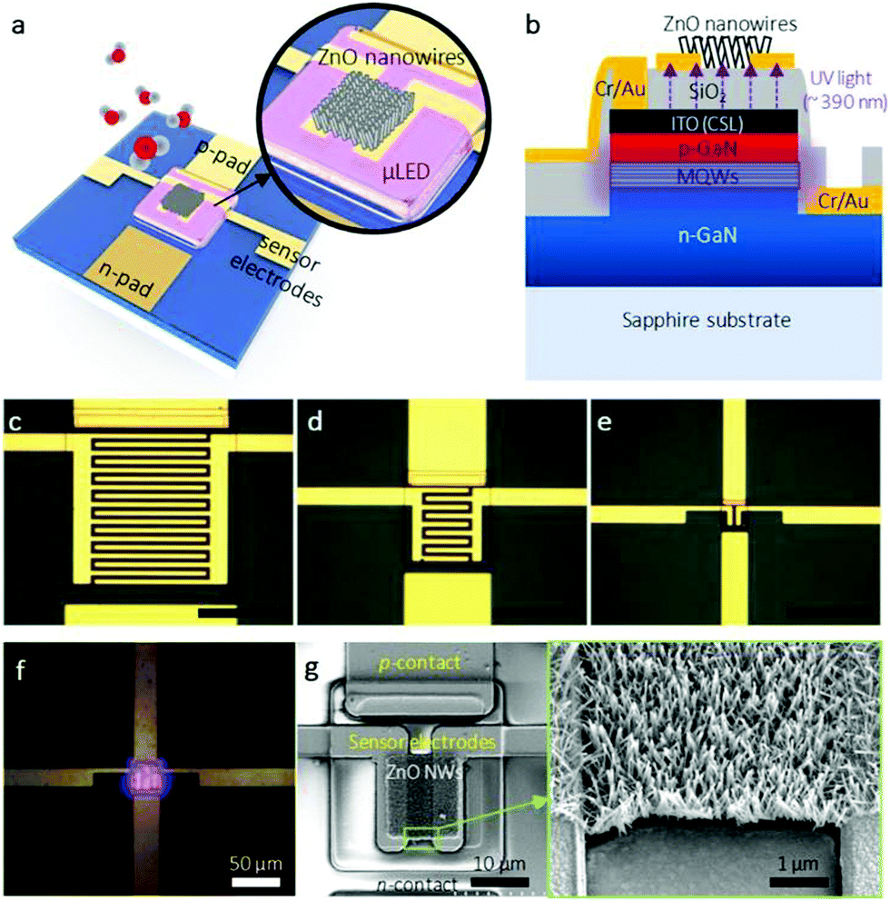 | ||
| Fig. 6 Illustration of a nanowire-based sensor with an integrated microscopic light source: (a) top view and (b) cross-sectional view. Optical microscopy images of the electrodes and microlight plate area (c–e) before and (f) after excitation of the LED. (g) SEM images of the gas-sensitive structures integrated over the microlight plate. Reprinted (adapted) from ref. 160, with permission from the American Chemical Society, 2020. | ||
Other types of integrated light sources in the visible spectrum for sensing applications have also been proposed previously, for instance, using vertical GaN-based nanowires. These structures showed potential for future 3D nano-LED arrays that could be valuable for building chemical sensors.162 Previous studies have also shown the integration of light sources into flexible substrates for optofluidic fluorescent sensors.163 These systems used microscale vertical cavity surface-emitting lasers (micro-VCSELs) with silicon photodiodes to achieve near-infrared light emitters. Authors reported the opto-mechanical properties of these flexible systems. Table 5 also shows other examples of on-chip integrated light sources.155,164–166 Among them, the new type of LED consisting of organic compound-based films that emit light in response to an electric current (OLED) is gaining interest in the field. This technology is younger than its more established LED counterparts, but it has reached significant progress in the past few years, especially in the near UV wavelength range,167 and could bring further advances in the on-chip integration of light sources for chemical sensors. Currently, the continuous improvements in OLEDs focus on achieving better EQEs in the UV-A range,168 better lifetimes, and emissions in the UVB and UVC wavelength regions.
5. Conclusions
The review summarized the recent advances in photoactive bare and composite materials for NO2 sensing at ppb concentrations, providing the fundamentals of photoactivated gas sensing and insights into the materials, synthetic methods, and enabling technologies for achieving light-activated gas microsensors. The discussion addressed the most common strategies to improve photoactivity in gas-sensitive materials, including incorporating surface vacancies in semiconductor materials and forming nanoscale interfaces based on metal–semiconductor or semiconductor–semiconductor junctions. The survey showed that semiconducting metal oxides (specifically ZnO), either with or without nanoscale interfaces, are the most representative materials in light-activated NO2 sensing. Among various photoactive semiconductors investigated and reported in the literature to date, results suggest that only specific systems, including ZnO, Pd–ZnO, and CdS–ZnO, provide significant responses to low NO2 concentrations (<10 ppb) with relatively fast response and recovery times (<1 min). However, new photoactive materials (e.g., TMDCs, organic semiconductors, and organo-functional structures) have proven to be promising systems for improving further the photoactive response to gases and volatiles, particularly when employed in combination with well-established metal oxide semiconductors, as their synergy adds robustness and stability to the system. The new material combination should also explore the use of Z-scheme heterojunctions (which have been less exploited in the gas sensing literature) as these systems promise an efficient charge separation and superior photoactivated response to chemical species. This new generation of gas-sensitive photoactive materials needs to focus further on improving and evaluating functional parameters such as selectivity, long-term stability, and humidity interference to provide a more realistic appraisal of photoactivated sensors’ performance for their practical application.Overall, future research on gas-sensitive photoactive materials needs to deepen into the experimental and computational design of interfaces, doping levels, and defects of the composite materials, rescuing and extrapolating the knowledge from other close areas such as photocatalysis and photonics. This, with the objective of bringing earth-abundant material combinations capable of delivering a photoactive response in the visible part of the solar spectrum to impact the power consumption and integration of multisensory systems positively. The availability of multisensory systems containing different photosensitive materials and/or activating lights could open the possibility for multivariable analysis and the use of pattern recognition concepts that are eventually essential to boost selectivity and pave the way for the applicability of these systems.
Conflicts of interest
There are no conflicts to declare.Acknowledgements
This work was supported by the Czech Science Foundation (GAČR), via Grant No. 20-20123S, and the MCIN/AEI/10.13039/501100011033, via Grants PID2019-107697RB-C42 (ERDF A way of making Europe), and RYC-2015-18296 from the Ramón y Cajal programme.References
- R. A. Potyrailo, Multivariable Sensors for Ubiquitous Monitoring of Gases in the Era of Internet of Things and Industrial Internet, Chem. Rev., 2016, 116, 11877–11923, DOI:10.1021/acs.chemrev.6b00187.
- J. L. Peel, R. Haeuber, V. Garcia, A. G. Russell and L. Neas, Impact of nitrogen and climate change interactions on ambient air pollution and human health, Biogeochemistry, 2013, 114, 121–134, DOI:10.1007/s10533-012-9782-4.
- R. W. Atkinson, B. K. Butland, H. R. Anderson and R. L. Maynard, Long-term concentrations of nitrogen dioxide and mortality, Epidemiology, 2018, 29, 460–472, DOI:10.1097/EDE.0000000000000847.
- J. C. Chow, Measurement methods to determine compliance with ambient air quality standards for suspended particles, J. Air Waste Manage. Assoc., 1995, 45, 320–382, DOI:10.1080/10473289.1995.10467369.
- E. G. Snyder, T. H. Watkins, P. A. Solomon, E. D. Thoma, R. W. Williams, G. S. W. Hagler, D. Shelow, D. A. Hindin, V. J. Kilaru and P. W. Preuss, The changing paradigm of air pollution monitoring, Environ. Sci. Technol., 2013, 47, 11369–11377, DOI:10.1021/es4022602.
- G. Korotcenkov and B. K. Cho, Engineering approaches for the improvement of conductometric gas sensor parameters: Part 1. Improvement of sensor sensitivity and selectivity (short survey), Sens. Actuators, B, 2013, 188, 709–728, DOI:10.1016/j.snb.2013.07.101.
- D. Karakaya, O. Ulucan and M. Turkan, Electronic Nose and Its Applications: A Survey, Int. J. Autom. Comput., 2020, 17, 179–209, DOI:10.1007/s11633-019-1212-9.
- Z. Chen, Z. Chen, Z. Song, W. Ye and Z. Fan, Smart gas sensor arrays powered by artificial intelligence, J. Semicond., 2019, 40, 111601, DOI:10.1088/1674-4926/40/11/111601.
- J. F. McAleer, P. T. Moseley, J. O. W. Norris, D. E. Williams, P. Taylor and B. C. Tofield, Tin oxide based gas sensors, Mater. Chem. Phys., 1987, 17, 577–583, DOI:10.1016/0254-0584(87)90017-4.
- N. Yamazoe, Toward innovations of gas sensor technology, Sens. Actuators, B, 2005, 108, 2–14, DOI:10.1016/j.snb.2004.12.075.
- G. Korotcenkov, Metal oxides for solid-state gas sensors: What determines our choice?, Mater. Sci. Eng., B, 2007, 139, 1–23, DOI:10.1016/j.mseb.2007.01.044.
- G. W. Hunter, S. Akbar, S. Bhansali, M. Daniele, P. D. Erb, K. Johnson, C.-C. Liu, D. Miller, O. Oralkan, P. J. Hesketh, P. Manickam and R. L. Vander Wal, Editors’ Choice–Critical Review—A Critical Review of Solid State Gas Sensors, J. Electrochem. Soc., 2020, 167, 037570, DOI:10.1149/1945-7111/ab729c.
- J. Saura, Gas-sensing properties of SnO2 pyrolytic films subjected to ultraviolet radiation, Sens. Actuators, B, 1994, 17, 211–214, DOI:10.1016/0925-4005(93)00874-X.
- E. Comini, G. Faglia and G. Sberveglieri, UV light activation of tin oxide thin films for NO2 sensing at low temperatures, Sens. Actuators, B, 2001, 78, 73–77, DOI:10.1016/S0925-4005(01)00796-1.
- J. D. Prades, R. Jimenez-Diaz, F. Hernandez-Ramirez, S. Barth, A. Cirera, A. Romano-Rodriguez, S. Mathur and J. R. Morante, Equivalence between thermal and room temperature UV light-modulated responses of gas sensors based on individual SnO2 nanowires, Sens. Actuators, B, 2009, 140, 337–341, DOI:10.1016/j.snb.2009.04.070.
- E. Espid and F. Taghipour, UV-LED Photo-activated Chemical Gas Sensors: A Review, Crit. Rev. Solid State Mater. Sci., 2017, 42, 416–432, DOI:10.1080/10408436.2016.1226161.
- R. Kumar, X. Liu, J. Zhang and M. Kumar, Room-Temperature Gas Sensors Under Photoactivation: From Metal Oxides to 2D Materials, Nano-Micro Lett., 2020, 12, 1–37, DOI:10.1007/s40820-020-00503-4.
- Z. Yuan, F. Yang, F. Meng, K. Zuo and J. Li, Research of Low-Power MEMS-Based Micro Hotplates Gas Sensor: A Review, IEEE Sens. J., 2021, 21, 18368–18380, DOI:10.1109/JSEN.2021.3088440.
- N. Markiewicz, O. Casals, C. Fabrega, I. Gràcia, C. Cané, H. S. Wasisto, A. Waag and J. D. Prades, Micro light plates for low-power photoactivated (gas) sensors, Appl. Phys. Lett., 2019, 114, 53508, DOI:10.1063/1.5078497.
- A. Kudo and Y. Miseki, Heterogeneous photocatalyst materials for water splitting, Chem. Soc. Rev., 2009, 38, 253–278, 10.1039/b800489g.
- S. K. Saraswat, D. D. Rodene and R. B. Gupta, Recent advancements in semiconductor materials for photoelectrochemical water splitting for hydrogen production using visible light, Renewable Sustainable Energy Rev., 2018, 89, 228–248, DOI:10.1016/j.rser.2018.03.063.
- Y. Tachibana, L. Vayssieres and J. R. Durrant, Artificial photosynthesis for solar water-splitting, Nat. Photonics, 2012, 68(6), 511–518, DOI:10.1038/nphoton.2012.175.
- J. L. White, M. F. Baruch, J. E. Pander III, Y. Hu, I. C. Fortmeyer, J. E. Park, T. Zhang, K. Liao, J. Gu, Y. Yan, T. W. Shaw, E. Abelev and A. B. Bocarsly, Light-Driven Heterogeneous Reduction of Carbon Dioxide: Photocatalysts and Photoelectrodes, Chem. Rev., 2015, 115, 12888–12935, DOI:10.1021/ACS.CHEMREV.5B00370.
- A. Hernández-Ramírez and I. Medina-Ramírez, Semiconducting Materials, in Photocatalytic Semicond. Synth. Charact. Environ. Appl., Springer International Publishing, 2015, pp. 1–40 DOI:10.1007/978-3-319-10999-2_1.
- Z. Zhang and J. T. Yates, Band bending in semiconductors: Chemical and physical consequences at surfaces and interfaces, Chem. Rev., 2012, 112, 5520–5551, DOI:10.1021/cr3000626.
- L. Wei, C. Yu, Q. Zhang, H. Liu and Y. Wang, TiO2-based heterojunction photocatalysts for photocatalytic reduction of CO2 into solar fuels, J. Mater. Chem. A, 2018, 6, 22411–22436, 10.1039/c8ta08879a.
- N. Serpone and A. V. Emeline, Semiconductor photocatalysis - Past, present, and future outlook, J. Phys. Chem. Lett., 2012, 3, 673–677, DOI:10.1021/jz300071j.
- X. Wang, F. Wang, Y. Sang and H. Liu, Full-spectrum solar-light-activated photocatalysts for light–chemical energy conversion, Adv. Energy Mater., 2017, 7, 1700473, DOI:10.1002/aenm.201700473.
- J. Li and N. Wu, Semiconductor-based photocatalysts and photoelectrochemical cells for solar fuel generation: A review, Catal. Sci. Technol., 2015, 5, 1360–1384, 10.1039/c4cy00974f.
- A. Giberti, B. Fabbri, A. Gaiardo, V. Guidi and C. Malagù, Resonant photoactivation of cadmium sulfide and its effect on the surface chemical activity, Appl. Phys. Lett., 2014, 104, 222102, DOI:10.1063/1.4881179.
- R. McCluney, Introduction to Radiometry and Photometry, Sens. Rev., 1998, 18, 159–163, DOI:10.1108/sr.1998.08718dae.002.
- V. Lordi, P. Erhart and D. Åberg, Charge carrier scattering by defects in semiconductors, Phys. Rev. B: Condens. Matter Mater. Phys., 2010, 81, 235204, DOI:10.1103/PhysRevB.81.235204.
- M. Shatalov, A. Lunev, X. Hu, O. Bilenko, I. Gaska, W. Sun, J. Yang, A. Dobrinsky, Y. Bilenko, R. Gaska and M. Shur, Performance and applications of deep UV LED, Int. J. High Speed Electron. Syst., 2012 DOI:10.1142/S0129156412500115.
- F. Xu and H. P. Ho, Light-activated metal oxide gas sensors: A review, Micromachines, 2017, 8, 333, DOI:10.3390/mi8110333.
- M. Grätzel, Photoelectrochemical cells, Nature, 2001, 414, 338–344, DOI:10.1038/35104607.
- A. G. Tamirat, J. Rick, A. A. Dubale, W. N. Su and B. J. Hwang, Using hematite for photoelectrochemical water splitting: A review of current progress and challenges, Nanoscale Horiz., 2016, 1, 243–267, 10.1039/c5nh00098j.
- A. Ghicov and P. Schmuki, Self-ordering electrochemistry: A review on growth and functionality of TiO2 nanotubes and other self-aligned MOx structures, Chem. Commun., 2009, 2791–2808, 10.1039/b822726h.
- Q. Lu, Y. Yu, Q. Ma, B. Chen and H. Zhang, 2D Transition-Metal-Dichalcogenide-Nanosheet-Based Composites for Photocatalytic and Electrocatalytic Hydrogen Evolution Reactions, Adv. Mater., 2016, 28, 1917–1933, DOI:10.1002/adma.201503270.
- A. Y. Polyakov, D. A. Kozlov, V. A. Lebedev, R. G. Chumakov, A. S. Frolov, L. V. Yashina, M. N. Rumyantseva and E. A. Goodilin, Gold Decoration and Photoresistive Response to Nitrogen Dioxide of WS2 Nanotubes, Chem. – Eur. J., 2018, 24, 18952–18962, DOI:10.1002/chem.201803502.
- Y. Zhou, C. Gao and Y. Guo, UV assisted ultrasensitive trace NO2 gas sensing based on few-layer MoS2 nanosheet-ZnO nanowire heterojunctions at room temperature, J. Mater. Chem. A, 2018, 6, 10286–10296, 10.1039/c8ta02679c.
- M. J. Mleczko, A. C. Yu, C. M. Smyth, V. Chen, Y. Cheol Shin, S. Chatterjee, Y.-C. Tsai, Y. Nishi, R. M. Wallace and E. Pop, Contact Engineering High-Performance n-Type MoTe2 Transistors, Nano Lett., 2021, 55, 11, DOI:10.1021/acs.nanolett.9b02497.
- L. A. Burton, T. J. Whittles, D. Hesp, W. M. Linhart, J. M. Skelton, B. Hou, R. F. Webster, G. O’Dowd, C. Reece, D. Cherns, D. J. Fermin, T. D. Veal, V. R. Dhanak and A. Walsh, Electronic and optical properties of single crystal SnS2: An earth-abundant disulfide photocatalyst, J. Mater. Chem. A, 2016, 4, 1312–1318, 10.1039/c5ta08214e.
- X. Zhang, Y. L. Chen, R. S. Liu and D. P. Tsai, Plasmonic photocatalysis, Rep. Prog. Phys., 2013, 76, 046401, DOI:10.1088/0034-4885/76/4/046401.
- H. Wang, L. Zhou, Y. Liu, F. Liu, X. Liang, F. Liu, Y. Gao, X. Yan and G. Lu, UV-activated ultrasensitive and fast reversible ppb NO2 sensing based on ZnO nanorod modified by constructing interfacial electric field with In2O3 nanoparticles, Sens. Actuators, B, 2020, 305, 127498, DOI:10.1016/j.snb.2019.127498.
- H. Wang, J. Bai, M. Dai, K. Liu, Y. Liu, L. Zhou, F. Liu, F. Liu, Y. Gao, X. Yan and L. Geyu, Visible light activated excellent NO2 sensing based on 2D/2D ZnO/g-C3N4 heterojunction composites, Sens. Actuators, B, 2020, 304, 127287, DOI:10.1016/J.SNB.2019.127287.
- E. Gonzalez, E. Llobet, A. Romero, X. Vilanova and A. New, Approach to NO2 Gas Sensing Based on Pulsed UV Light and FFT Analysis Using MOX Sensors, IEEE Sens. J., 2020, 20, 397–404, DOI:10.1109/JSEN.2019.2942490.
- K. Davis, R. Yarbrough, M. Froeschle, J. White and H. Rathnayake, Band gap engineered zinc oxide nanostructures: Via a sol-gel synthesis of solvent driven shape-controlled crystal growth, RSC Adv., 2019, 9, 14638–14648, 10.1039/c9ra02091h.
- V. Pawar, P. K. Jha, S. K. Panda, P. A. Jha and P. Singh, Band-Gap Engineering in ZnO Thin Films: A Combined Experimental and Theoretical Study, Phys. Rev. Appl., 2018, 9, 054001, DOI:10.1103/PhysRevApplied.9.054001.
- J. Wang, Y. Shen, X. Li, Y. Xia and C. Yang, Synergistic effects of UV activation and surface oxygen vacancies on the room-temperature NO2 gas sensing performance of ZnO nanowires, Sens. Actuators, B, 2019, 298, 126858, DOI:10.1016/j.snb.2019.126858.
- G. Li, H. Zhang, L. Meng, Z. Sun, Z. Chen, X. Huang and Y. Qin, Adjustment of oxygen vacancy states in ZnO and its application in ppb-level NO2 gas sensor, Sci. Bull., 2020, 65(2020), 1650–1658, DOI:10.1016/j.scib.2020.05.027.
- Y. Xia, L. Zhou, J. Yang, P. Du, L. Xu and J. Wang, Highly Sensitive and Fast Optoelectronic Room-Temperature NO2 Gas Sensor Based on ZnO Nanorod-Assembled Macro-/Mesoporous Film, ACS Appl. Electron. Mater., 2020, 2, 580–589, DOI:10.1021/acsaelm.9b00810.
- C. Zhang, X. Geng, H. Liao, C. J. Li and M. Debliquy, Room-temperature nitrogen-dioxide sensors based on ZnO1-x coatings deposited by solution precursor plasma spray, Sens. Actuators, B, 2017, 242, 102–111, DOI:10.1016/j.snb.2016.11.024.
- F. Wang, C. Di Valentin and G. Pacchioni, Rational Band Gap Engineering of WO3 Photocatalyst for Visible light Water Splitting, ChemCatChem, 2012, 4, 476–478, DOI:10.1002/cctc.201100446.
- F. Wang, C. Di Valentin and G. Pacchioni, Electronic and structural properties of WO3: A systematic hybrid DFT study, J. Phys. Chem. C, 2011, 115, 8345–8353, DOI:10.1021/jp201057m.
- C. Zhang, A. Boudiba, P. De Marco, R. Snyders, M. G. Olivier and M. Debliquy, Room temperature responses of visible-light illuminated WO3 sensors to NO2 in sub-ppm range, Sens. Actuators, B, 2013, 181, 395–401, DOI:10.1016/j.snb.2013.01.082.
- T. Suzuki, H. Watanabe, T. Ueno, Y. Oaki and H. Imai, Significant Increase in Band Gap and Emission Efficiency of In2O3 Quantum Dots by Size-Tuning around 1 nm in Supermicroporous Silicas, Langmuir, 2017, 33, 3014–3017, DOI:10.1021/acs.langmuir.6b04181.
- Z. G. Zhang, X. X. Wang, J. Zhang, M. Yu, J. C. Zhang, H. Di Zhang and Y. Z. Long, Recent advances in 1D micro- and nanoscale indium oxide structures, J. Alloys Compd., 2018, 752, 359–375, DOI:10.1016/j.jallcom.2018.04.188.
- X.-X. Wang, H.-Y. Li and X. Guo, Flexible and transparent sensors for ultra-low NO2 detection at room temperature under visible light illumination, J. Mater. Chem. A, 2020, 8, 14482–14490, 10.1039/d0ta02934c.
- X. Geng, D. Lahem, C. Zhang, C. J. Li, M. G. Olivier and M. Debliquy, Visible light enhanced black NiO sensors for ppb-level NO2 detection at room temperature, Ceram. Int., 2019, 45, 4253–4261, DOI:10.1016/j.ceramint.2018.11.097.
- E. Wu, Y. Xie, B. Yuan, H. Zhang, X. Hu, J. Liu and D. Zhang, Ultrasensitive and Fully Reversible NO2 Gas Sensing Based on p-Type MoTe2 under Ultraviolet Illumination, ACS Sens., 2018, 3, 1719–1726, DOI:10.1021/acssensors.8b00461.
- Q. Zhang, G. Xie, M. Xu, Y. Su, H. Tai, H. Du and Y. Jiang, Visible light-assisted room temperature gas sensing with ZnO-Ag heterostructure nanoparticles, Sens. Actuators, B, 2018, 259, 269–281, DOI:10.1016/j.snb.2017.12.052.
- J. Wang, C. Hu, Y. Xia and S. Komarneni, Highly sensitive, fast and reversible NO2 sensors at room-temperature utilizing nonplasmonic electrons of ZnO/Pd hybrids, Ceram. Int., 2020, 46, 8462–8468, DOI:10.1016/j.ceramint.2019.12.081.
- Z. Yang, L. Guo, B. Zu, Y. Guo, T. Xu and X. Dou, CdS/ZnO Core/Shell Nanowire-Built Films for Enhanced Photodetecting and Optoelectronic Gas-Sensing Applications, Adv. Opt. Mater., 2014, 2, 738–745, DOI:10.1002/adom.201400086.
- G. Lu, J. Xu, J. Sun, Y. Yu, Y. Zhang and F. Liu, UV-enhanced room temperature NO2 sensor using ZnO nanorods modified with SnO2 nanoparticles, Sens. Actuators, B, 2012, 162, 82–88, DOI:10.1016/j.snb.2011.12.039.
- R. R. Kumar, T. Murugesan, A. Dash, C. H. Hsu, S. Gupta, A. Manikandan, A. kumar Anbalagan, C. H. Lee, N. H. Tai, Y. L. Chueh and H. N. Lin, Ultrasensitive and light-activated NO2 gas sensor based on networked MoS2/ZnO nanohybrid with adsorption/desorption kinetics study, Appl. Surf. Sci., 2021, 536, 147933, DOI:10.1016/j.apsusc.2020.147933.
- W. C. Lu, S. S. Kumar, Y. C. Chen, C. M. Hsu and H. N. Lin, Au/Cu2O/ZnO ternary nanocomposite for low concentration NO2 gas sensing at room temperature, Mater. Lett., 2019, 256, 126657, DOI:10.1016/j.matlet.2019.126657.
- X. Geng, C. Zhang, Y. Luo and M. Debliquy, Preparation and characterization of CuxO1-y@ZnO1-α nanocomposites for enhanced room-temperature NO2 sensing applications, Appl. Surf. Sci., 2017, 401, 248–255, DOI:10.1016/j.apsusc.2017.01.014.
- A. Giampiccolo, D. M. Tobaldi, S. G. Leonardi, B. J. Murdoch, M. P. Seabra, M. P. Ansell, G. Neri and R. J. Ball, Sol gel graphene/TiO2 nanoparticles for the photocatalytic-assisted sensing and abatement of NO2, Appl. Catal., B, 2019, 243, 183–194, DOI:10.1016/j.apcatb.2018.10.032.
- W. Li, J. Guo, L. Cai, W. Qi, Y. Sun, J. L. Xu, M. Sun, H. Zhu, L. Xiang, D. Xie and T. Ren, UV light irradiation enhanced gas sensor selectivity of NO2 and SO2 using rGO functionalized with hollow SnO2 nanofibers, Sens. Actuators, B, 2019, 290, 443–452, DOI:10.1016/j.snb.2019.03.133.
- Y. Huang, W. Jiao, Z. Chu, G. Ding, M. Yan, X. Zhong and R. Wang, Ultrasensitive room temperature ppb-level NO2 gas sensors based on SnS2/rGO nanohybrids with P-N transition and optoelectronic visible light enhancement performance, J. Mater. Chem. C, 2019, 7, 8616–8625, 10.1039/c9tc02436k.
- P. G. Su, J. H. Yu, I. C. Chen, H. C. Syu, S. W. Chiu and T. I. Chou, Detection of ppb-level NO2 gas using a portable gas-sensing system with a Fe2O3/MWCNTs/WO3 sensor using a pulsed-UV-LED, Anal. Methods, 2019, 11, 973–979, 10.1039/c8ay02500b.
- P. G. Su and J. H. Yu, Enhanced NO2 gas-sensing properties of Au-Ag bimetal decorated MWCNTs/WO3 composite sensor under UV-LED irradiation, Sens. Actuators, A, 2020, 303, 111718, DOI:10.1016/j.sna.2019.111718.
- K. O. Ukoba, A. C. Eloka-Eboka and F. L. Inambao, Review of nanostructured NiO thin film deposition using the spray pyrolysis technique, Renewable Sustainable Energy Rev., 2018, 82, 2900–2915, DOI:10.1016/j.rser.2017.10.041.
- C. Zhang, G. Liu, X. Geng, K. Wu and M. Debliquy, Metal oxide semiconductors with highly concentrated oxygen vacancies for gas sensing materials: A review, Sens. Actuators, A, 2020, 309, 112026, DOI:10.1016/j.sna.2020.112026.
- M. S. Tyagi, Physics of Schottky Barrier Junctions, in Metal-semiconductor Schottky barrier junctions and their applications, Springer, US, 1984, pp. 1–60 DOI:10.1007/978-1-4684-4655-5_1.
- Z. Li and X. Meng, Recent development on palladium enhanced photocatalytic activity: A review, J. Alloys Compd., 2020, 830, 154669, DOI:10.1016/j.jallcom.2020.154669.
- T. Su, Q. Shao, Z. Qin, Z. Guo and Z. Wu, Role of Interfaces in Two-Dimensional Photocatalyst for Water Splitting, ACS Catal., 2018, 8, 2253–2276, DOI:10.1021/acscatal.7b03437.
- X. Li, J. Yu, M. Jaroniec and X. Chen, Cocatalysts for selective photoreduction of CO2 into solar fuels, Chem. Rev., 2019, 119, 3962–4179, DOI:10.1021/acs.chemrev.8b00400.
- L. G. Devi and R. Kavitha, A review on plasmonic metal-TiO2 composite for generation, trapping, storing and dynamic vectorial transfer of photogenerated electrons across the Schottky junction in a photocatalytic system, Appl. Surf. Sci., 2016, 360, 601–622, DOI:10.1016/j.apsusc.2015.11.016.
- A. Wang, S. Wu, J. Dong, R. Wang, J. Wang, J. Zhang, S. Zhong and S. Bai, Interfacial facet engineering on the Schottky barrier between plasmonic Au and TiO2 in boosting the photocatalytic CO2 reduction under ultraviolet and visible light irradiation, Chem. Eng. J., 2021, 404, 127145, DOI:10.1016/j.cej.2020.127145.
- S. Zhong, Y. Xi, Q. Chen, J. Chen and S. Bai, Bridge engineering in photocatalysis and photoelectrocatalysis, Nanoscale, 2020, 12, 5764–5791, 10.1039/c9nr10511e.
- V. Kumar, S. O’Donnell, B. Zoellner, J. Martinez, G. Wang and P. A. Maggard, Interfacing Plasmonic Nanoparticles with Ferroelectrics for Hot-Carrier-Driven Photocatalysis: Impact of Schottky Barrier Height, ACS Appl. Energy Mater., 2019, 2, 7690–7699, DOI:10.1021/acsaem.9b01682.
- C. Clavero, Plasmon-induced hot-electron generation at nanoparticle/metal-oxide interfaces for photovoltaic and photocatalytic devices, Nat. Photonics, 2014, 8, 95–103, DOI:10.1038/nphoton.2013.238.
- M. R. Khan, T. W. Chuan, A. Yousuf, M. N. K. Chowdhury and C. K. Cheng, Schottky barrier and surface plasmonic resonance phenomena towards the photocatalytic reaction: Study of their mechanisms to enhance photocatalytic activity, Catal. Sci. Technol., 2015, 5, 2522–2531, 10.1039/c4cy01545b.
- D. W. Kim, K. H. Park, S. H. Lee, C. Fàbrega, J. D. Prades and J. W. Jang, Plasmon expedited response time and enhanced response in gold nanoparticles-decorated zinc oxide nanowire-based nitrogen dioxide gas sensor at room temperature, J. Colloid Interface Sci., 2021, 582, 658–668, DOI:10.1016/j.jcis.2020.08.082.
- C. Chen, Q. Zhang, G. Xie, M. Yao, H. Pan, H. Du, H. Tai, X. Du and Y. Su, Enhancing visible light-activated NO2 sensing properties of Au NPs decorated ZnO nanorods by localized surface plasmon resonance and oxygen vacancies, Mater. Res. Express, 2020, 7, 015924, DOI:10.1088/2053-1591/ab6b64.
- J. Wang, S. Fan, Y. Xia, C. Yang and S. Komarneni, Room-temperature gas sensors based on ZnO nanorod/Au hybrids: Visible-light-modulated dual selectivity to NO2 and NH3, J. Hazard. Mater., 2020, 381, 120919, DOI:10.1016/j.jhazmat.2019.120919.
- C. Langhammer, Z. Yuan, I. Zorić and B. Kasemo, Plasmonic properties of supported Pt and Pd nanostructures, Nano Lett., 2006, 6, 833–838, DOI:10.1021/nl060219x.
- J. Su, G.-D. Li, X.-H. Li and J.-S. Chen, 2D/2D Heterojunctions for Catalysis, Adv. Sci., 2019, 6, 1801702, DOI:10.1002/ADVS.201801702.
- J. Low, J. Yu, M. Jaroniec, S. Wageh and A. A. Al-Ghamdi, Heterojunction Photocatalysts, Adv. Mater., 2017, 29, 1601694, DOI:10.1002/adma.201601694.
- D. Huang, S. Chen, G. Zeng, X. Gong, C. Zhou, M. Cheng, W. Xue, X. Yan and J. Li, Artificial Z-scheme photocatalytic system: What have been done and where to go?, Coord. Chem. Rev., 2019, 385, 44–80, DOI:10.1016/J.CCR.2018.12.013.
- L. Zhang and M. Jaroniec, Toward designing semiconductor-semiconductor heterojunctions for photocatalytic applications, Appl. Surf. Sci., 2018, 430, 2–17, DOI:10.1016/j.apsusc.2017.07.192.
- H. Wang, L. Zhang, Z. Chen, J. Hu, S. Li, Z. Wang, J. Liu and X. Wang, Semiconductor heterojunction photocatalysts: Design, construction, and photocatalytic performances, Chem. Soc. Rev., 2014, 43, 5234–5244, 10.1039/c4cs00126e.
- J. S. Jang, H. G. Kim and J. S. Lee, Heterojunction semiconductors: A strategy to develop efficient photocatalytic materials for visible light water splitting, Catal. Today, 2012, 270–277, DOI:10.1016/j.cattod.2011.07.008.
- Q. Xu, L. Zhang, J. Yu, S. Wageh, A. A. Al-Ghamdi and M. Jaroniec, Direct Z-scheme photocatalysts: Principles, synthesis, and applications, Mater. Today, 2018, 21, 1042–1063, DOI:10.1016/j.mattod.2018.04.008.
- D. Han, L. Zhai, F. Gu and Z. Wang, Highly sensitive NO2 gas sensor of ppb-level detection based on In2O3 nanobricks at low temperature, Sens. Actuators, B, 2018, 262, 655–663, DOI:10.1016/j.snb.2018.02.052.
- J. Zhao, M. Hu, Y. Liang, Q. Li, X. Zhang and Z. Wang, A room temperature sub-ppm NO2 gas sensor based on WO3 hollow spheres, New J. Chem., 2020, 44, 5064–5070, 10.1039/c9nj06384f.
- N. Coppedè, M. Villani, R. Mosca, S. Iannotta, A. Zappettini and D. Calestani, Low Temperature Sensing Properties of a Nano Hybrid Material Based on ZnO Nanotetrapods and Titanyl Phthalocyanine, Sensors, 2013, 13, 3445–3453, DOI:10.3390/s130303445.
- J. Huang, Y. Kang, T. Yang, Y. Wang and S. Wang, Preparation of polythiophene/WO3 organic-inorganic hybrids and their gas sensing properties for NO2 detection at low temperature, J. Nat. Gas Chem., 2011, 20, 403–407, DOI:10.1016/S1003-9953(10)60196-X.
- W. Liu, L. Xu, K. Sheng, C. Chen, X. Zhou, B. Dong, X. Bai, S. Zhang, G. Lu and H. Song, APTES-functionalized thin-walled porous WO3 nanotubes for highly selective sensing of NO2 in a polluted environment, J. Mater. Chem. A, 2018, 6, 10976–10989, 10.1039/c8ta02452a.
- A. T. Mane, S. T. Navale and V. B. Patil, Room temperature NO2 gas sensing properties of DBSA doped PPy-WO3 hybrid nanocomposite sensor, Org. Electron., 2015, 19, 15–25, DOI:10.1016/j.orgel.2015.01.018.
- M. W. G. Hoffmann, J. D. Prades, L. Mayrhofer, F. Hernandez-Ramirez, T. T. Järvi, M. Moseler, A. Waag and H. Shen, Highly selective SAM-nanowire hybrid NO2 sensor: Insight into charge transfer dynamics and alignment of frontier molecular orbitals, Adv. Funct. Mater., 2014, 24, 595–602, DOI:10.1002/adfm.201301478.
- M. Tomić, Z. Fohlerova, I. Gràcia, E. Figueras, C. Cané and S. Vallejos, UV-light activated APTES modified WO3-x nanowires sensitive to ethanol and nitrogen dioxide, Sens. Actuators, B, 2020, 129046, DOI:10.1016/j.snb.2020.129046.
- M. Reddeppa, S. B. Mitta, B. G. Park, S. G. Kim, S. H. Park and M. D. Kim, DNA-CTMA functionalized GaN surfaces for NO2 gas sensor at room temperature under UV illumination, Org. Electron., 2019, 65, 334–340, DOI:10.1016/j.orgel.2018.11.038.
- M. A. Chougule, S. Sen and V. B. Patil, Polypyrrole-ZnO hybrid sensor: Effect of camphor sulfonic acid doping on physical and gas sensing properties, Synth. Met., 2012, 162, 1598–1603, DOI:10.1016/j.synthmet.2012.07.002.
- C. Wang, M. Yang, L. Liu, Y. Xu, X. Zhang, X. Cheng, S. Gao, Y. Gao and L. Huo, One-step synthesis of polypyrrole/Fe2O3 nanocomposite and the enhanced response of NO2 at low temperature, J. Colloid Interface Sci., 2020, 560, 312–320, DOI:10.1016/j.jcis.2019.10.076.
- L. Mazeina, F. K. Perkins, V. M. Bermudez, S. P. Arnold and S. M. Prokes, Functionalized Ga2O3 nanowires as active material in room temperature capacitance-based gas sensors, Langmuir, 2010, 26, 13722–13726, DOI:10.1021/la101760k.
- F. A. Harraz, M. Faisal, M. Jalalah, A. A. Almadiy, S. A. Al-Sayari and M. S. Al-Assiri, Conducting polythiophene/α-Fe2O3 nanocomposite for efficient methanol electrochemical sensor, Appl. Surf. Sci., 2020, 508, 145226, DOI:10.1016/j.apsusc.2019.145226.
- M. Hijazi, M. Rieu, V. Stambouli, G. Tournier, J. P. Viricelle and C. Pijolat, Ambient temperature selective ammonia gas sensor based on SnO2-APTES modifications, Sens. Actuators, B, 2018, 256, 440–447, DOI:10.1016/j.snb.2017.10.036.
- B. T. Raut, M. A. Chougule, S. R. Nalage, D. S. Dalavi, S. Mali, P. S. Patil and V. B. Patil, CSA doped polyaniline/CdS organic-inorganic nanohybrid: Physical and gas sensing properties, Ceram. Int., 2012, 38, 5501–5506, DOI:10.1016/j.ceramint.2012.03.064.
- M. Procek, A. Stolarczyk and T. Pustelny, Impact of Temperature and UV Irradiation on Dynamics of NO2 Sensors Based on ZnO Nanostructures, Nanomaterials, 2017, 7, 312, DOI:10.3390/nano7100312.
- Y. Shen, X. Zhong, J. Zhang, T. Li, S. Zhao, B. Cui, D. Wei, Y. Zhang and K. Wei, In-situ growth of mesoporous In2O3 nanorod arrays on a porous ceramic substrate for ppb-level NO2 detection at room temperature, Appl. Surf. Sci., 2019, 498, 143873, DOI:10.1016/j.apsusc.2019.143873.
- D. Gu, X. Wang, W. Liu, X. Li, S. Lin, J. Wang, M. N. Rumyantseva, A. M. Gaskov and S. A. Akbar, Visible-light activated room temperature NO2 sensing of SnS2 nanosheets based chemiresistive sensors, Sens. Actuators, B, 2020, 305, 127455, DOI:10.1016/j.snb.2019.127455.
- R. Kumar, N. Goel and M. Kumar, UV-Activated MoS2 Based Fast and Reversible NO2 Sensor at Room Temperature, ACS Sens., 2017, 2, 1744–1752, DOI:10.1021/acssensors.7b00731.
- L. Sacco, S. Forel, I. Florea and C. S. Cojocaru, Ultra-sensitive NO2 gas sensors based on single-wall carbon nanotube field effect transistors: Monitoring from ppm to ppb level, Carbon, 2020, 157, 631–639, DOI:10.1016/j.carbon.2019.10.073.
- F. Yavari, E. Castillo, H. Gullapalli, P. M. Ajayan and N. Koratkar, High sensitivity detection of NO2 and NH3 in air using chemical vapor deposition grown graphene, Appl. Phys. Lett., 2012, 100, 203120, DOI:10.1063/1.4720074.
- S. Cui, H. Pu, E. C. Mattson, Z. Wen, J. Chang, Y. Hou, C. J. Hirschmugl and J. Chen, Ultrasensitive chemical sensing through facile tuning defects and functional groups in reduced graphene oxide, Anal. Chem., 2014, 86, 7516–7522, DOI:10.1021/ac501274z.
- Y. Zhou, C. Zou, X. Lin and Y. Guo, UV light activated NO2 gas sensing based on Au nanoparticles decorated few-layer MoS2 thin film at room temperature, Appl. Phys. Lett., 2018, 113, 082103, DOI:10.1063/1.5042061.
- Y. Xia, J. Wang, J. L. Xu, X. Li, D. Xie, L. Xiang and S. Komarneni, Confined Formation of Ultrathin ZnO Nanorods/Reduced Graphene Oxide Mesoporous Nanocomposites for High-Performance Room-Temperature NO2 Sensors, ACS Appl. Mater. Interfaces, 2016, 8, 35454–35463, DOI:10.1021/acsami.6b12501.
- R. Kumar, O. Al-Dossary, G. Kumar and A. Umar, Zinc oxide nanostructures for NO2 gas–sensor applications: A review, Nano-Micro Lett., 2015, 7, 97–120, DOI:10.1007/s40820-014-0023-3.
- Á. Morales-García, A. Macià Escatllar, F. Illas and S. T. Bromley, Understanding the interplay between size, morphology and energy gap in photoactive TiO2 nanoparticles, Nanoscale, 2019, 11, 9032–9041, 10.1039/c9nr00812h.
- M. Guan, C. Xiao, J. Zhang, S. Fan, R. An, Q. Cheng, J. Xie, M. Zhou, B. Ye and Y. Xie, Vacancy associates promoting solar-driven photocatalytic activity of ultrathin bismuth oxychloride nanosheets, J. Am. Chem. Soc., 2013, 135, 10411–10417, DOI:10.1021/ja402956f.
- M. Kong, Y. Li, X. Chen, T. Tian, P. Fang, F. Zheng and X. Zhao, Tuning the relative concentration ratio of bulk defects to surface defects in TiO2 nanocrystals leads to high photocatalytic efficiency, J. Am. Chem. Soc., 2011, 133, 16414–16417, DOI:10.1021/ja207826q.
- S. Bai, N. Zhang, C. Gao and Y. Xiong, Defect engineering in photocatalytic materials, Nano Energy, 2018, 53, 296–336, DOI:10.1016/j.nanoen.2018.08.058.
- Z. Fang, B. Bueken, D. E. De Vos and R. A. Fischer, Defect-Engineered Metal-Organic Frameworks, Angew. Chem., Int. Ed., 2015, 54, 7234–7254, DOI:10.1002/anie.201411540.
- J. Wang, J. Deng, Y. Li, H. Yuan and M. Xu, ZnO nanocrystal-coated MoS2 nanosheets with enhanced ultraviolet light gas sensitive activity studied by surface photovoltage technique, Ceram. Int., 2020, 46, 11427–11431, DOI:10.1016/j.ceramint.2020.01.157.
- E. Espid, B. Adeli and F. Taghipour, Enhanced Gas Sensing Performance of Photo-Activated, Pt-Decorated, Single-Crystal ZnO Nanowires, J. Electrochem. Soc., 2019, 166, H3223–H3230, DOI:10.1149/2.0301905jes.
- M. A. H. Khan, B. Thomson, R. Debnath, A. Rani, A. Motayed and M. V. Rao, Reliable anatase-titania nanoclusters functionalized GaN sensor devices for UV assisted NO2 gas-sensing in ppb level, Nanotechnology, 2020, 31, 155504, DOI:10.1088/1361-6528/ab6685.
- A. V. Nikam, B. L. V. Prasad and A. A. Kulkarni, Wet chemical synthesis of metal oxide nanoparticles: A review, CrystEngComm, 2018, 20, 5091–5107, 10.1039/C8CE00487K.
- A. Tofanello, S. Shen, F. L. De Souza and L. Vayssieres, Strategies to improve the photoelectrochemical performance of hematite nanorod-based photoanodes, APL Mater., 2020, 8, 040905, DOI:10.1063/5.0003146.
- J. Wang, M. Yu, X. Li and Y. Xia, UV-enhanced NO2 gas sensing properties of polystyrene sulfonate functionalized ZnO nanowires at room temperature, Inorg. Chem. Front., 2019, 6, 176–183, 10.1039/c8qi01110a.
- R. Gao, Z. Ying, W. Sheng and P. Zheng, Gas sensors based on ZnO/silk fibroin film for nitrogen dioxide detection under UV light at room temperature, Mater. Lett., 2018, 229, 210–212, DOI:10.1016/j.matlet.2018.07.018.
- X. Geng, J. You, J. Wang and C. Zhang, Visible light assisted nitrogen dioxide sensing using tungsten oxide - Graphene oxide nanocomposite sensors, Mater. Chem. Phys., 2017, 191, 114–120, DOI:10.1016/j.matchemphys.2017.01.046.
- J. Hu, C. Zou, Y. Su, M. Li, X. Ye, B. Cai, E. S. W. Kong, Z. Yang and Y. Zhang, Light-assisted recovery for a highly-sensitive NO2 sensor based on RGO-CeO2 hybrids, Sens. Actuators, B, 2018, 270, 119–129, DOI:10.1016/j.snb.2018.05.027.
- X. Geng, C. Zhang, Y. Luo, H. Liao and M. Debliquy, Light assisted room-temperature NO2 sensors with enhanced performance based on black SnO1-α@ZnO1-β@SnO2-γ nanocomposite coatings deposited by solution precursor plasma spray, Ceram. Int., 2017, 43, 5990–5998, DOI:10.1016/j.ceramint.2017.01.136.
- N. Yi, Z. Cheng, H. Li, L. Yang, J. Zhu, X. Zheng, Y. Chen, Z. Liu, H. Zhu and H. Cheng, Stretchable, ultrasensitive, and low-temperature NO2 sensors based on MoS2@rGO nanocomposites, Mater. Today Phys., 2020, 15, 100265, DOI:10.1016/j.mtphys.2020.100265.
- C. P. Burke-Govey and N. O. V. Plank, Review of hydrothermal ZnO nanowires: Toward FET applications, J. Vac. Sci. Technol., B, 2013, 31, 06F101, DOI:10.1116/1.4821801.
- J. Bao, I. Shalish, Z. Su, R. Gurwitz, F. Capasso, X. Wang and Z. Ren, Photoinduced oxygen release and persistent photoconductivity in ZnO nanowires, Nanoscale Res. Lett., 2011, 6, 1–7, DOI:10.1186/1556-276X-6-404.
- M. Kumar, A. V. Agrawal, R. Kumar, S. Venkatesan, A. Zakhidov, G. Yang, J. Bao and M. Kumar, Photoactivated Mixed In-Plane and Edge-Enriched p-Type MoS2 Flake-Based NO2 Sensor Working at Room Temperature, ACS Sens., 2018, 3, 998–1004, DOI:10.1021/acssensors.8b00146.
- T.-C. Chen, Y.-C. Yang, H.-L. Liu, C.-M. Yang, M. Meyyappan and C.-S. Lai, The Effect of Monolayer Graphene on the UV Assisted NO2 Sensing and Recovery at Room Temperature, Proceedings, 2017, 1, 461, DOI:10.3390/proceedings1040461.
- L. Qi, L. Yu, Z. Liu, F. Guo, Y. Qiang Gu and X. Fan, An enhanced optoelectronic NO2 gas sensors based on direct growth ZnO nanowalls in situ on porous rGO, J. Alloys Compd., 2018, 749, 244–249, DOI:10.1016/j.jallcom.2018.03.298.
- S. W. Fan, A. K. Srivastava and V. P. Dravid, UV-activated room-temperature gas sensing mechanism of polycrystalline ZnO, Appl. Phys. Lett., 2009, 95, 142106, DOI:10.1063/1.3243458.
- Y. Nagasawa and A. Hirano, A review of AlGaN-based deep-ultraviolet light-emitting diodes on sapphire, Appl. Sci., 2018, 8, 1264, DOI:10.3390/app8081264.
- H. S. Wasisto, J. D. Prades, J. Gülink and A. Waag, Beyond solid-state lighting: Miniaturization, hybrid integration, and applications of GaN nano-and micro-LEDs, Appl. Phys. Rev., 2019, 6, 41315, DOI:10.1063/1.5096322.
- W. Zhang and W. Jiang, UV treatment improved the quality of postharvest fruits and vegetables by inducing resistance, Trends Food Sci. Technol., 2019, 92, 71–80, DOI:10.1016/j.tifs.2019.08.012.
- N. G. Yeh, C. H. Wu and T. C. Cheng, Light-emitting diodes-Their potential in biomedical applications, Renewable Sustainable Energy Rev., 2010, 8, 2161–2166, DOI:10.1016/j.rser.2010.02.015.
- O. Autin, C. Romelot, L. Rust, J. Hart, P. Jarvis, J. MacAdam, S. A. Parsons and B. Jefferson, Evaluation of a UV-light emitting diodes unit for the removal of micropollutants in water for low energy advanced oxidation processes, Chemosphere, 2013, 92, 745–751, DOI:10.1016/j.chemosphere.2013.04.028.
- J. Liang, L. Sun, S. Wang, Q. Sun, B. Devakumar and X. Huang, Filling the cyan gap toward full-visible-spectrum LED lighting with Ca2LaHf2Al3O12:Ce3+ broadband green phosphor, J. Alloys Compd., 2020, 836, 155469, DOI:10.1016/j.jallcom.2020.155469.
- S. Nagai, K. Yamada, A. Hirano, M. Ippommatsu, M. Ito, N. Morishima, K. Aosaki, Y. Honda, H. Amano and I. Akasaki, Development of highly durable deep-ultraviolet AlGaN-based LED multichip array with hemispherical encapsulated structures using a selected resin through a detailed feasibility study, Jpn. J. Appl. Phys., 2016, 55, 082101, DOI:10.7567/JJAP.55.082101.
- V. Poher, N. Grossman, G. T. Kennedy, K. Nikolic, H. X. Zhang, Z. Gong, E. M. Drakakis, E. Gu, M. D. Dawson, P. M. W. French, P. Degenaar and M. A. A. Neil, Micro-LED arrays: A tool for two-dimensional neuron stimulation, J. Phys. D: Appl. Phys., 2008, 41, 94014, DOI:10.1088/0022-3727/41/9/094014.
- D. Y. Won, H. M. Kim, Y. J. Oh, M.-C. Nguyen, R. Choi, J.-M. Myoung and H. Yoon, Minimizing Residual Images of Amorphous Indium Gallium Zinc Oxide Thin-Film Transistor-Based Flexible Organic Light-Emitting Diode Displays by Controlling Oxygen Partial Pressure, J. Nanosci. Nanotechnol., 2020, 20, 6916–6919, DOI:10.1166/jnn.2020.18805.
- C. Feng, X. Zheng, R. Xu, Y. Zhou, H. Hu, T. Guo, J. Ding, L. Ying and F. Li, Highly efficient inkjet printed flexible organic light-emitting diodes with hybrid hole injection layer, Org. Electron., 2020, 85, 105822, DOI:10.1016/j.orgel.2020.105822.
- C. A. Hurni, A. David, M. J. Cich, R. I. Aldaz, B. Ellis, K. Huang, A. Tyagi, R. A. Delille, M. D. Craven, F. M. Steranka and M. R. Krames, Bulk GaN flip-chip violet light-emitting diodes with optimized efficiency for high-power operation, Appl. Phys. Lett., 2015, 106, 031101, DOI:10.1063/1.4905873.
- J. Schanda, Light Emitting Diodes, in Encyclopedia of Modern Optics Five-Volume Set, Elsevier Inc., 2004, pp. 522–526 DOI:10.1016/B0-12-369395-0/01258-6.
- S. Li, S. Fündling, Ü. Sökmen, R. Neumann, S. Merzsch, P. Hinze, T. Weimann, U. Jahn, A. Trampert, H. Riechert, E. Peiner, H.-H. Wehmann and A. Waag, GaN nanorods and LED structures grown on patterned Si and AlN/Si substrates by selective area growth, Phys. Status Solidi C, 2010, 7, 2224–2226, DOI:10.1002/pssc.200983457.
- K. Yamada, Y. Nagasawa, S. Nagai, A. Hirano, M. Ippommatsu, K. Aosaki, Y. Honda, H. Amano and I. Akasaki, Study on the Main-Chain Structure of Amorphous Fluorine Resins for Encapsulating AlGaN-Based DUV-LEDs, Phys. Status Solidi Appl. Mater. Sci., 2018, 215, 1700525, DOI:10.1002/pssa.201700525.
- S. I. Inoue, T. Naoki, T. Kinoshita, T. Obata and H. Yanagi, Light extraction enhancement of 265 nm deep-ultraviolet light-emitting diodes with over 90 mW output power via an AlN hybrid nanostructure, Appl. Phys. Lett., 2015, 106, 131104, DOI:10.1063/1.4915255.
- M. Kneissl, T.-Y. Seong, J. Han and H. Amano, The emergence and prospects of deep-ultraviolet light-emitting diode technologies, Nat. Photonics, 2019, 13, 233–244, DOI:10.1038/s41566-019-0359-9.
- O. Casals, N. Markiewicz, C. Fabrega, I. Gràcia, C. Cane, H. S. Wasisto, A. Waag and J. D. Prades, A Parts per Billion (ppb) Sensor for NO2 with Microwatt (μW) Power Requirements Based on Micro Light Plates, ACS Sens., 2019, 4, 822–826, DOI:10.1021/acssensors.9b00150.
- I. Cho, Y. C. Sim, M. Cho, Y. H. Cho and I. Park, Monolithic Micro Light-Emitting Diode/Metal Oxide Nanowire Gas Sensor with Microwatt-Level Power Consumption, ACS Sens., 2020, 5, 563–570, DOI:10.1021/acssensors.9b02487.
- C. L. Hsu, L. F. Chang and T. J. Hsueh, Light-activated humidity and gas sensing by ZnO nanowires grown on LED at room temperature, Sens. Actuators, B, 2017, 249, 265–277, DOI:10.1016/j.snb.2017.04.083.
- S. Mariana, J. Gülink, G. Hamdana, F. Yu, K. Strempel, H. Spende, N. Yulianto, T. Granz, J. D. Prades, E. Peiner, H. S. Wasisto and A. Waag, Vertical GaN Nanowires and Nanoscale Light-Emitting-Diode Arrays for Lighting and Sensing Applications, ACS Appl. Nano Mater., 2019, 2, 4133–4142, DOI:10.1021/acsanm.9b00587.
- D. Kang, B. Gai, B. Thompson, S. M. Lee, N. Malmstadt and J. Yoon, Flexible Opto-Fluidic Fluorescence Sensors Based on Heterogeneously Integrated Micro-VCSELs and Silicon Photodiodes, ACS Photonics, 2016, 3, 912–918, DOI:10.1021/acsphotonics.6b00080.
- J. Herrnsdorf, J. J. D. McKendry, S. Zhang, E. Xie, R. Ferreira, D. Massoubre, A. M. Zuhdi, R. K. Henderson, I. Underwood, S. Watson, A. E. Kelly, E. Gu and M. D. Dawson, Active-matrix GaN micro light-emitting diode display with unprecedented brightness, IEEE Trans. Electron Devices, 2015, 62, 1918–1925, DOI:10.1109/TED.2015.2416915.
- M. Tchernycheva, A. Messanvi, A. de Luna Bugallo, G. Jacopin, P. Lavenus, L. Rigutti, H. Zhang, Y. Halioua, F. Julien, J. Eymery and C. Durand, Integrated photonic platform based on InGaN/GaN nanowire emitters and detectors, Nano Lett., 2014, 14(6), 3515–3520 CrossRef CAS PubMed.
- C. Goßler, C. Bierbrauer, R. Moser, M. Kunzer, K. Holc, W. Pletschen, K. Köhler, J. Wagner, M. Schwaerzle, P. Ruther, O. Paul, J. Neef, D. Keppeler, G. Hoch, T. Moser and U. T. Schwarz, GaN-based micro-LED arrays on flexible substrates for optical cochlear implants, J. Phys. D: Appl. Phys., 2014, 47, 205401, DOI:10.1088/0022-3727/47/20/205401.
- T. Miwa, S. Kubo, K. Shizu, T. Komino, C. Adachi and H. Kaji, Blue organic light-emitting diodes realizing external quantum efficiency over 25% using thermally activated delayed fluorescence emitters, Sci. Rep., 2017, 7, 1–8, DOI:10.1038/s41598-017-00368-5.
- Y. Luo, S. Li, Y. Zhao, C. Li, Z. Pang, Y. Huang, M. Yang, L. Zhou, X. Zheng, X. Pu and Z. Lu, An Ultraviolet Thermally Activated Delayed Fluorescence OLED with Total External Quantum Efficiency over 9%, Adv. Mater., 2020, 32, 2001248, DOI:10.1002/adma.202001248.
| This journal is © The Royal Society of Chemistry 2021 |