
 Open Access Article
 This Open Access Article is licensed under a
 Creative Commons Attribution 3.0 Unported Licence
Optical field coupling in ZnO nanorods decorated with silver plasmonic nanoparticles†
Mojtaba
Gilzad Kohan‡
 a,
Shujie
You‡
a,
Andrea
Camellini‡
b,
Isabella
Concina
a,
Margherita
Zavelani Rossi
bc and
Alberto
Vomiero
*ad
a,
Shujie
You‡
a,
Andrea
Camellini‡
b,
Isabella
Concina
a,
Margherita
Zavelani Rossi
bc and
Alberto
Vomiero
*ad
aDivision of Materials Science, Department of Engineering Sciences and Mathematics, Luleå University of Technology, 97187 Luleå, Sweden. E-mail: alberto.vomiero@ltu.se
bDipartimento di Energia, Politecnico di Milano, Via G. Ponzio 34/3, Milano I-20133, Italy
cIFN-CNR, piazza L. Da Vinci 32, 20133 Milano, Italy
dDepartment of Molecular Sciences and Nanosystems, Ca' Foscari University of Venice, Via Torino 155, 30172 Venezia Mestre, Italy. E-mail: alberto.vomiero@unive.it
First published on 19th August 2021
Abstract
Characterizing carrier redistribution due to optical field modulation in a plasmonic hot-electron/semiconductor junction can be used to raise the framework for harnessing the carrier decay of plasmonic metals in more efficient conversion systems. In this work we comprehensively studied the carrier redistribution mechanisms of a 1-dimensional (1D) metal-semiconductor Schottky architecture, holding the dual feature of a hot-electron plasmonic system and a simple metal/semiconductor junction. We obtained a strongly enhanced external quantum efficiency (EQE) of the plasmonic Ag decorated ZnO semiconductor in both the band-edge region of ZnO and the corresponding plasmonic absorption profile of the Ag NPs (visible region). Simultaneously, the insertion of an insulating Al2O3 intermediate layer between Ag NPs and ZnO resulted in a parallel distinction of the two main non-radiative carrier transfer mechanisms of plasmonic NPs, i.e. direct electron transfer (DET) and plasmonic induced resonance energy transfer (PIRET). The multi-wavelength transient pump–probe spectroscopy indicated the very fast plasmonic radiative transfer dynamics of the system in <500 fs below 389 nm. We demonstrate a 13% increase of photogenerated current in ZnO upon visible irradiation as a result of non-radiative plasmonic hot-electron injection from Ag NPs. Overall, our device encompasses several effective solutions for designing a plasmonic system featuring non-radiative electron–electron plasmonic dephasing and high photoconversion efficiencies.
Introduction
Synergetic design of hybrid semiconductor nanostructures can promote new high-throughput functionalities with improved optoelectronic properties. Interaction of noble metal NPs with semiconductors under electromagnetic optical fields can achieve the exploitation of various physical processes in several different fields such as energy harvesting, photocatalysis and biological sensing.1–3Through strong light interaction with plasmonic NPs, a conventional junction of the noble metal NPs/semiconductors can give rise to several unique phenomena such as electric field enhancement, tunable light absorption (from visible to infrared region of the spectrum) and generation of hot-electron–hole pairs through the decay of localized surface plasmon resonance (LSPR). The decay of the resonant oscillation in plasmonic NPs normally takes place as (i) radiative emissions and/or (ii) non-radiative relaxation via electron–electron and electron–phonon interactions. The term hot-electron generation is generally attributed to the non-radiative relaxation mode of plasmonic NPs.4,5 In a Schottky junction of plasmonic NPs and semiconductors, the LSPR generated hot-electrons can possibly overcome the barrier offset of plasmonic NPs/semiconductor and travel into the conduction band of the neighboring semiconductor.6 Generally, the transfer of the non-radiative hot-electrons from plasmonic NPs to semiconductors in a solid-state Schottky system is highlighted by two distinct mechanisms. (i) The main route is expressed via direct electron transfer (DET) of the high energy hot-electrons (between 1 and 4 eV for Ag and Au NPs with different shapes and sizes) that are not in thermodynamic equilibrium into the conduction band of the adjacent semiconductor.7–9 (ii) The second mechanism includes the induction of the electron–hole dipoles in the semiconductor from the large photo-excited electron–hole dipoles that were generated in the plasmonic NPs. This latter mechanism is generally referred to as plasmon induced resonance energy transfer (PIRET).10–12
Harnessing of the non-radiative hot-electrons, resulting from LSPR dephasing of plasmonic NPs, can substantially increase light absorption, resulting in boosting of the photoconversion efficiency of the energy conversion systems. In particular, coupling the LSPR decay of plasmonic NPs with wide-bandgap semiconductors that pose low absorption in the visible range can lead to very efficient absorption of light, higher carrier densities and lower recombination rates.13–15
Zinc oxide (ZnO) a direct wide-bandgap metal oxide (MOx) semiconductor, is a remarkable material for short-wavelength photonic devices due to its high excitonic binding energy (60 meV at room temperature) and large energy gap (3.0–3.2 eV).16 Conventionally, ZnO has been considered as a suitable substrate for the growth of other nanostructured alloys like GaN. The high quality of its bulk crystals, grown in a variety of structures, and its strong luminescence in the UV region have attracted numerous research studies on this material.17 Among all morphologies, the 1D ZnO nanorods (NRs) and nanowires (NWs) are some of the most extensively studied structures.18 Due to their high aspect ratio (length/width), it is possible to separate the length scales for light absorption and exciton diffusion, hence representing a favorable configuration in solar light harvesting devices (for instance, solar cells, photodetectors and photoelectrochemical cells) with efficient charge collection and current generation.19 Despite the outstanding performance of ZnO in optoelectronic applications, several shortcomings undermine the potential performance of ZnO NRs and NWs in different photonic fields. While 1D structures of ZnO permit enhanced carrier transport and large mean free path for electrons, the visible-light driven application of ZnO NRs are rather limited due to their bandgap energy of ∼3.2 eV which makes ZnO only responsive to UV light.20 In addition, low temperature and the wet-chemical environment of the hydrothermally grown ZnO NRs and NWs tend to create severe native and intrinsic defects, which in turn can cause uncontrolled conductivity, lattice imperfections and fast electron–hole recombination rate.21 Therefore, several solutions have been targeted to either modify the intrinsic crystalline properties of ZnO (annealing in different atmospheres and plasma treatment) and/or broaden its absorption profile through the design of a combinatorial composite system via metal and non-metal doping.22–27 In particular, coupling with noble metals is an effective approach to enhance the visible light absorption of wide bandgap semiconductors, which inherently can also assist the passivation of their intrinsic defects.6,7 For instance, deposition of Au/Pt NPs on ZnO NRs usually results in enlarged photocurrent, enhancement in ZnO UV emission and a simultaneous suppression of visible emission.28,29 The improved performance is often attributed to passivation of ZnO surface defects and coupling of metal NP surface plasmon resonance with ZnO.
Silver NPs with a plasmonic resonant absorption at a wavelength around 400 nm (∼3.1 eV depending on their size and shape), are potential materials to be coupled with ZnO30 due to their strong electromagnetic field enhancement properties.31 However, considering their low chemical stability, Ag NPs are less studied compared to many other metal NPs. Besides, the size of Ag NPs and deposition methods can both affect the coupling between Ag LSPR and ZnO.32–34
One study investigated the effect of fabricating a plasmonic Schottky junction of TiO2 with Ag/Au in a Kretschmann coupling geometry.35 The obtained photoconversion device indicated the superior hot-electron injection properties of Ag/Al2O3/TiO2 compared to the Au/Al2O3/TiO2 counterpart devices. The thin Al2O3 insulating layer in the junctions presented a very effective approach to reduce the fast electron–hole recombination between Ag LSPR and TiO2 and yet permits the tunneling mechanism of hot carriers. In particular, several studies reported the remarkable photocatalytic performance of the ZnO/Ag LSPR nanostructured systems in enhanced photo-degradation of standard dyes under UV and visible light illuminations.36–38 However, a precise investigation on the optical field interaction of a simple solid-state Schottky plasmonic system has not yet been addressed.
In this framework, we spotlight both competitive ways of carrier transfer as in a (i) typical Schottky junction, where photoexcited charges are transferred from ZnO to Ag due to their Fermi energy band offset and (ii) LSPR decay hot-electron transfer from Ag NPs to ZnO NRs. Later on, both DET and PIRET processes, as two major non-radiative hot-electron transfer mechanisms, were investigated. Herein we have proposed an architecture for our samples that can promote the dual functionality of plasmonic light harvesting and concurrently presents a Schottky junction between the Ag NPs and the ZnO NRs. The direct effect of light harvesting in Ag NPs, in which photon absorption and carrier generation occurs specifically in plasmonic NPs were distinctively studied by insertion of an insulating Al2O3 intermediate layer in between the Ag NPs and the ZnO NRs. The homogeneous passivating Al2O3 layer was intended to minimize the effect of DET processes and to only permit the dipole–dipole coupling mechanisms and possible contributions of high-energy electron tunneling from Ag to ZnO NRs. Ultra-fast transient absorption spectroscopy enabled insight into the excited carrier dynamics, showing the role of the LSPR and injection of hot-electrons. This, together with time resolved photoluminescence (TRPL) disclosed the optical response of the building blocks and highlighted the effect of the coupling between the semiconductor and the plasmonic metal NPs in non-LSPR mechanisms. Further, we pinpointed the electric response of the samples which results from the electron–electron decay mechanism of Ag NPs LSPR to ZnO and translated into photocurrent generation in photoconversion devices. Overall, this work presents an in-depth comprehensive study over the photophysics of the ZnO/Ag NPs Schottky junction and gives important hints for efficient architectures for future light harvesting/detection devices, combining high photon absorption with high carrier transfer/generation.
Results and discussion
Two sets of samples were considered for the systematic analysis of the hybrid system: (i) ZnO NRs/Ag NPs to highlight the effect of direct contact between Ag NPs and ZnO semiconductor; (ii) ZnO NRs/Al2O3/Ag NPs to investigate the role of the Al2O3 intermediate layer as a physical barrier to inhibit the direct charge injection between Ag NPs and NRs. This work includes some major studies toward investigation and distinction of the plasmonic carrier transfer dynamics of the plasmonic system Fig. 1(a)via several techniques which will be discussed further in the results. The SEM images of ZnO/Ag NPs sample in Fig. 1(b) show the morphology of the ZnO NRs on the FTO substrate. The NR array exhibits a perpendicular growth direction on FTO with the typical hexagonal cross-section of each NR. The as-prepared ZnO NRs present an overall diameter of 70–190 nm. The low concentration of the Ag NPs can be detected on the surface of the NRs in Fig. 1(b) and (d). The ZnO/Ag sample was decorated with a “less than 1 monolayer thick” homogeneous coverage of Ag NPs. The density of Ag NPs is so low that we can exclude any self-interaction between neighboring NPs and reduce the possibility of hot-spot formation due to NP–NP contact. This is a critical point to obtain a correct interpretation of the optical data and to infer the photo-induced charge dynamics. The overall length of the ZnO NRs corresponding to the 3 hours of hydrothermal growth is estimated to be around ∼1.5 μm (Fig. 1(c)). EDS analysis in a selected area of the tip of a single NR (90 × 90 nm2 in size), where Ag NPs were observable, detected the presence of Zn, O and Ag, with no other impurities on the samples (Fig. 1(d) and inset). The obtained XRD pattern confers the epitaxial growth of the single crystalline ZnO NRs along the (002) crystalline direction (Fig. 1(e)). Notably, the preferred crystalline orientation of the NRs is an important feature of 1D semiconductors in optoelectronic systems, promoting higher carrier transfer properties. The morphological characterization of the samples with Al2O3 interfacial layer is presented in Fig. S1 (ESI†). The Al2O3 film was homogenously deposited on the ZnO NRs, preserving the 1D morphology of the samples. The distribution of the Ag NPs on the ZnO/Al2O3/Ag NPs sample resembles the counterpart sample without an interfacial Al2O3 layer, although a few Ag NP aggregates were observed. The Ag NPs aggregates visible on the Al2O3 coated sample can be explained by the possible changes in the surface roughness of the NRs after Al2O3 deposition. The thickness of the deposited Al2O3 layer is determined through Rutherford backscattering (RBS) from a flat silicon substrate covered during the same ALD deposition (Fig. S2, ESI†). The RBS data are collected in channeling condition with respect to the substrate, which enables distinct detection of the thin Al2O3 layer. The XRUMP code simulation of the RBS spectrum evaluated the thickness of ∼4 nm of the Al2O3 layer conformally deposited over the substrate (Fig. S2, ESI†). Diffuse-reflectance spectra of the samples prior and after deposition of the Ag NPs are presented in Fig. 2(a). The as-prepared bare ZnO NRs exhibit high reflection in the visible region while the reflection has a steep drop around 375 nm corresponding to the optical absorption edge of ZnO NRs. | ||
| Fig. 1 (a) Schematic illustration of the (1) direct electron transfer and (2) dipole–dipole carrier transfer mechanisms in ZnO and plasmonic Ag system. (b) SEM image of the ZnO NRs decorated with Ag NPs. (c) Cross-section view of the grown ZnO on the FTO substrate. (d) High resolution SEM image shows the distribution of the Ag NPs on the surface of NRs. (inset) EDS results indicates the presence of Ag NPs on ZnO NRs. (e) The XRD pattern of the ZnO/Ag NPs sample. The reflection peaks labeled with asterisks (*) in the XRD pattern of the samples arise from the FTO substrate underneath. | ||
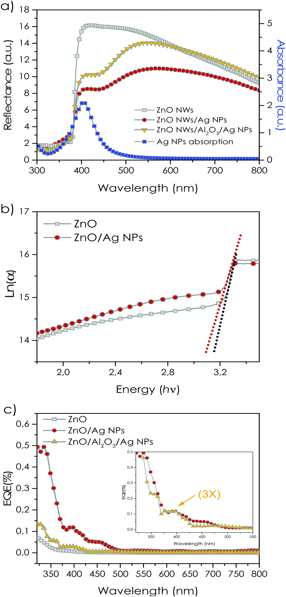 | ||
| Fig. 2 (a) Diffused reflectance of ZnO/Ag NPs, and ZnO/Al2O3/Ag NPs and bare ZnO NRs. The blue curve corresponds to absorption of Ag NPs in ethanol. (b) Urbach energy changes of the ZnO NRs samples before and after Ag NPs uptake. (c) External quantum efficiency of the ZnO/Ag NPs and ZnO/Al2O3/Ag NPs with respect to bare ZnO NRs (the EQE curve of the ZnO/Al2O3/Ag NPs sample is scaled up for clarity). | ||
The strong reflection in the region 400–800 nm is most likely due to the strong light scattering induced by the disordered NR array. As expected, the deposition of the Al2O3 layer on the samples did not result in any appreciable change of the ZnO NR absorption edge (Fig. S3, ESI†). The as-prepared Ag NPs present a typical sharp LSPR peak centred at around 405 nm. In agreement with SEM analysis (Fig. 1(b–d)) and the obtained LSPR position of the Ag NPs we determined the average size of the Ag NPs to be around 5–40 nm. After uptake of the Ag NPs on the samples, the corresponding LSPR absorption of Ag NPs creates a shoulder in the reflectance spectra of the ZnO NR films. In this regard, both ZnO/Ag NPs and ZnO/Al2O3 4 nm Ag−1 NPs exhibit the corresponding LSPR absorption peak of the Ag NPs in their reflectance spectra at around 420 nm. The slight shift of the positions of the LSPR characteristic absorption maximum in the absorption spectrum of the Ag NPs dispersed in ethanol (405 nm) and in the ZnO/Ag NPs composites (420 nm) can be attributed to the change of the Ag NP dielectric constant environmental medium.5
Fig. 2(b) shows the logarithm curve of the absorption coefficient (α) of the ZnO NRs before and after deposition of Ag NPs. The absorption coefficient is calculated using diffused reflectance spectra, taking into account the scattering effect of NRs. Considering the relation below, the Urbach energy (Eu) (band tail energy) can be obtained from the slope of the ln![[thin space (1/6-em)]](https://www.rsc.org/images/entities/char_2009.gif) (α) against the incident photon energy (hν).
(α) against the incident photon energy (hν).
| α = α0exp(hν/Eu) | (1) |
The Eu at the absorption edge of ZnO NRs (∼3.2 eV) is slightly modified by the uptake of the Ag NPs. The calculated Eu values indicated a slight increase from ∼0.075 eV to ∼0.097 eV for bare ZnO NR and Ag NP deposited samples, respectively. The increase in Eu values after deposition of the Ag NPs can be ascribed either to (i) the band-bending effect of the conduction band in ZnO due to the alignment of the Fermi energy level of Ag NPs and ZnO (originating the Schottky junction), or to (ii) the increase in the concentration of charge trapping sites at the surface of ZnO NRs after Ag uptake.39,40 Overall, our results suggest that the band tail energy, after deposition of Ag NPs on ZnO NRs is slightly enhanced.
The external quantum efficiency (EQE) of the samples under monochromatic light irradiation highlights the generation of free charge carriers, which depends on the behaviour of each constituent (ZnO NRs or Ag NPs) in the samples.
The presence of the Al2O3 spacer layer may modify the transfer of photogenerated charges between Ag NPs and ZnO NRs, making it worth investigating both the samples under monochromatic light irradiation (Fig. 2(c)).
In the range of 300–500 nm, the ZnO/Ag NP sample is characterized by EQE nearly ∼2.5 times larger than bare ZnO NRs. A downward tail can be observed in the EQE profile of the samples in the UV region below 350 nm in agreement with the absorption edge of the bare ZnO. The EQE curve of the ZnO/Ag NP sample exhibits a broad resonance peak between 375 and 500 nm with a maximum at ∼400 nm, corresponding to the LSPR absorption profile of the Ag NPs (Fig. 2(a)). These results clearly indicated the hot-electron LSPR transfer processes taking place from Ag NPs towards ZnO NRs, which can be translated into a combination of plasmonic charge injection mechanism via DET and PIRET to the ZnO conduction band. Based on the obtained EQE profile for the ZnO/Ag NP sample, coupling of Ag NPs to the ZnO NRs amounts to a drastic increase in the EQE values in both UV and visible regions distinctively from 375 to 500 nm which can support the field enhancement effect of Ag NPs on ZnO NRs. Interestingly, the ZnO/Al2O3/Ag NP sample shows a well-defined resonant peak between 370 and 430 nm corresponding to the Ag NP LSPR peak. Although, the overall EQE trend of the sample with 4 nm passivating Al2O3 is relatively smaller compared to the ZnO/Ag NPs sample (the EQE curve of the ZnO/Al2O3/Ag NP sample is scaled up in the inset of Fig. 2(c) for a more direct comparison). Here we have to consider that the passivating intermediate Al2O3 layer has dramatically reduced the DET injection mechanism and the corresponding resonant peak centered at 380 nm, can be assigned mainly to the PIRET dipole–dipole coupling process from Ag NPs to ZnO NRs. The 4 nm thick insulating Al2O3 layer decreases the probability of the tunnelling mechanism in this case, minimizing the DET process and emphasizing the effect of the dipole–dipole coupling. The different responses allow us to have a first indication of the predominant effect of DET over PIRET.
A typical steady state PL spectrum from ZnO NRs is shown in Fig. 3(a) (grey curve), which includes two parts: a sharp emission in the UV region centred at 376 nm (near band-edge emission, NBE) and a broad emission band in the visible region from 420 to 750 nm, centred at around 600 nm. The visible emission of ZnO is usually attributed to defect related emission (DLE) and comprises emission bands from interstitial Zn and oxygen, or vacancies. After uptake of Ag NPs, the ZnO UV-emission drops by around 80%; meantime the intensity of visible emission notably increases. We attributed the observed quenching of the NBE PL emission of the ZnO NRs to the non-radiative Förster resonance energy transfer (FRET) from the band-edge of the ZnO NRs to the red-shifted Ag NP light absorber.41 Furthermore, the centre of the visible emission red shifts by 25 nm, to 625 nm. We assigned the red shift of the visible broad band emission in this sample to the increase in the joint density of the states due to LSPR excitation of Ag NPs contributing to the energy levels of ZnO defect states as a result of the FRET absorption of emitted PL by Ag NPs decorating the surface of ZnO NRs. The PL quantum yield (QY) of as-prepared ZnO NRs and after surface modification is reported in Table S1 (ESI†). The QY was calculated by the total emission divided by the absorption at 325 nm. All samples show decreased emission after surface modification. The values in Table S1 (ESI†) further clarify that the decrease in QY is mainly due to the changes of the QY of visible emission (450 to 750 nm), since the QY from UV emission in most of the samples are around 0.1%. The surface modification lowers the QY(DLE) from strongest to mildest as: Al2O3 (45%) > Ag NPs (33%) > Al2O3 + Ag NPs (25%). Since Al2O3 does not absorb light in the visible region and the ALD deposition was performed at low temperature (150 °C), which does not change the crystallinity of ZnO, the quenching of QY(DLE) in ZnO/Al2O3 can be ascribed to surface passivation. Hence, considering the obtained optical transmittance of the ZnO/Al2O3 sample (Fig. S3, ESI†), we can verify that the deposited Al2O3 layer does not modify the energy band states in ZnO NRs. This effect is solely important for justification of the dipole–dipole PIRET transfer mechanism explained further in the current yield of the samples.
 | ||
| Fig. 3 (a) PL of the bare ZnO NRs and ZnO NRs/Ag NPs sample (λex = 325 nm) and (b) DLE life-time spectra of the samples before and after Ag NPs deposition. | ||
The drop of QY(DLE) in ZnO/Ag NPs is probably due to the absorption of Ag NPs as in Fig. 2. Interestingly, the change of QY(DLE) in ZnO/Al2O3/Ag NPs is lower than single modification of Al2O3 or Ag NPs. In this regard, the decay of the visible emission from the samples were studied using the time-resolved PL (TRPL) at room temperature to understand the changes of the surface trapped carriers of ZnO NRs. The TRPL decay curves of ZnO defect emission of the samples before and after decoration with Ag NPs are shown in the Fig. 3(b) and the calculated values of the lifetime are collected in Table 1. The direct contact of the Ag NPs with ZnO NRs (ZnO/Ag NPs sample) resulted in a slight increase of the average PL decay time-constant (τav), suggesting the transfer of the charges from ZnO to Ag NPs and increasing the pathway dynamics of the radiative electron recombination. In contrast, ZnO/Al2O3/Ag NPs sample presented a negligible change of τav indicating that the 4 nm Al2O3 layer can significantly block the transfer of the charges from ZnO NRs to Ag NPs. The ZnO/Al2O3 sample presented a minor decrease on the τav as a result of surface passivation due to the 4 nm thick ALD Al2O3 thin layer. It can be noted that the average PL life-time of ZnO visible emission does not present drastic changes even after uptake of Ag NPs. The overall fast PL decay in this case can, confirm the premises of the non-radiative FRET processes between Ag NPs and ZnO NRs.42 Since the electron life-time is determined by both radiative and non-radiative pathways, we describe the changes of the DLE life-time due to surface modifications of ZnO using a well-known two-state trapping model for semiconductors, in which the life-time of trap states (τtr) is defined by43,44
 | (2) |
| Sample | τ 1 [ns] | A1 | τ 2 [ns] | A2 | τ 3 [ns] | A3 | τ av [ns] |
|---|---|---|---|---|---|---|---|
| ZnO NRs | 3.33 | 233 | 11.5 | 210 | 36.8 | 39 | 17.9 |
| ZnO NRs/Al2O3 | 2.85 | 220 | 10.6 | 218 | 31.5 | 47 | 16.5 |
| ZnONRs/Al2O3/AgNPs | 3.11 | 233 | 11.2 | 216 | 33.6 | 42 | 16.8 |
| ZnO NRs/Ag NPs | 3.20 | 244 | 11.5 | 211 | 40.2 | 33 | 18.4 |
We performed pump–probe experiments to investigate the excited carrier dynamics. We used pump pulses centered at 266 nm and a white light probe beam extending from 375 to 650 nm. The pump photon energy, i.e. 4.7 eV, allows the simultaneous excitation of both ZnO45 and Ag NPs via interband transition.46 It is worth noticing that transient behavior of Ag NPs photo-excited via interband absorption closely matches that obtained by resonant LSPR pumping (i.e. there is no significant difference in recorded data when pumping at 266 nm or at 400 nm, Fig. S5, ESI†).47 Even so, we only precluded the possibility of the interband excitation of the Ag NPs using this analysis, and the carrier redistribution behavior and the timeframe of the process is only qualitatively studied using the hybrid solid-state samples. In Fig. 4 we show the transient transmission (TT), ΔT/T datasets along with TT spectra at four probe delays to highlight the different spectral evolution of the two samples.
 | ||
| Fig. 4 Differential transmission ΔT/T spectra and two-dimensional maps of (a) and (b) bare ZnO NRs and (c) and (d) ZnO NRs decorated with Ag NPs. ΔT/T spectra are shown at probe delay of 0.2, 0.5, 2 and 50 ps. Insest in panels (a) and (c) are expanded in the 500–650 nm region. Yellow and blue contour lines in panels (b) and (d) correspond to surface levels at half value of the negative and positive peak values of the TT datasets. Colorbar range limits are adjusted to favor a comparison between the two datasets on a common scale. The same datasets with colorbars covering the full dynamic range of the ΔT/T signals can be found in the ESI† (Fig. S6). Pump wavelength is 266 nm (i.e. 4.7 eV). | ||
Right after photoexcitation we observe in bare ZnO NRs two significant spectral features (Fig. 4(a) and (b)): a photoinduced absorption band (PA, ΔT/T < 0) between 380 nm and 420 nm with a minimum at around 389 nm and a broad photobleaching band (PB, ΔT/T > 0) at longer wavelengths which is most probably associated with defect states.45 In less than 1 ps, the TT spectrum evolves significantly in the region near the BE where the signal reverses and appears as a PB (ΔT/T > 0) with complex transient spectra features (dark grey spectrum in Fig. 4(a)). After 2 ps only one peak at around 389 nm remains, and for longer time delays no significant spectral modification can be appreciated (compare continuous and dashed black lines in Fig. 4(a)). The TT spectrum is thus characterized by two PB contributions: one ascribed to PB of the BE transition, centered at 389 nm, and a broad tail ascribed to defect states in the visible region. In the ZnO/Ag sample within the first 300 fs (Fig. 4(c)), the TT spectrum resembles that of bare ZnO NRs, with a negative PA band peaked at 389 nm (with smaller amplitude) and a broad positive PB band in the 500–700 nm region. The TT evolution differs significantly from that of bare ZnO NRs in the following time delays: in the region near ZnO BE, the TT signal further reduces its amplitude but remains negative (orange area in Fig. 4(d)). In about 2 ps the TT signal reaches a stable condition with a negative band in the 380–500 nm region and a broad PB band in the 500–700 nm region (Fig. 4(c)). As opposed to ZnO NRs a stable isosbestic point (ΔT = 0) is observed around 500 nm.
Fig. 5 shows the TT dynamics of ZnO NRs and ZnO/Ag in the region of ZnO BE, at a wavelength corresponding to the minimum of the initial PA (i.e. 389 nm, Fig. 5(a)), and around the maximum of the PB defect region (575 nm in Fig. 5(b)). ZnO dynamics in the BE region shows a fast rise-time reaching its maximum within the temporal resolution limit of our setup (∼100 fs) and it is followed by a fast exponential decay. The change of sign that the TT dynamics takes place in less than 1 ps leaving a positive PB signal afterward with a slow decay component (longer than 100 ps). In the visible region, we observe a very fast rise time, consistent with trap states recombination (Fig. 5(b)). Note that two PB bands correspond to population filling of the energy levels associated with ZnO BE and DLE (visible region), as observed in PL (Fig. 3). The population filling is reached in 2 ps for the BE whereas it is instantaneous for defects. The ZnO/Ag TT dynamics at 575 nm is instead similar to that of the ZnO NRs sample, with a very fast rise time and a long decay component. Differently, the TT dynamic in the BE region shows a fast response of ZnO NRs in the first ∼300 fs, affected by a reduction in the signal amplitude, and big differences afterward (Fig. 5(a) and inset).
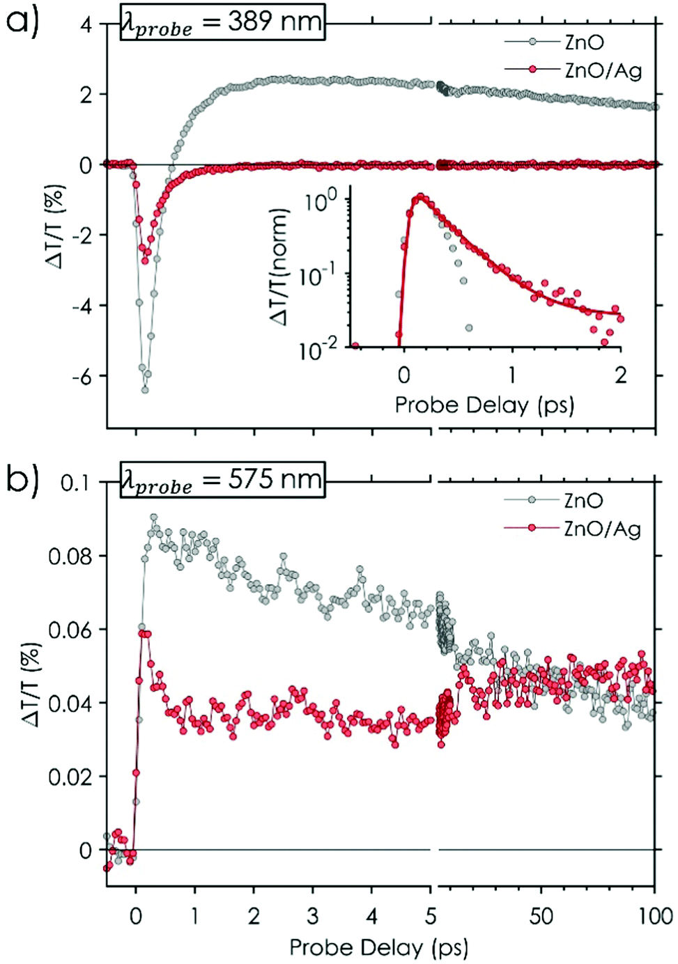 | ||
| Fig. 5 Differential transmission ΔT/T dynamics on 100 ps time scale for bare ZnO NRs (grey dots) and ZnO NRs/Ag NPs (red dots) at two probe wavelengths: (a) 389 nm and (b) 575 nm. Inset of panel (a) shows the normalized TT dynamics at 389 nm within the first 2 ps: ZnO/Ag dynamic is fitted by an exponential Ae−t/τ + y0 convolved with a Gaussian function having full width at half maximum corresponding to the temporal resolution of the setup (∼100 fs); decay constant of ZnO/Ag dynamics is ∼0.3 ps. Pump wavelength is 266 nm (i.e. 4.7 eV). | ||
The interpretation of the aforementioned complex spectral and temporal behaviors for the ZnO NRs sample relies on the pump induced modifications of the dielectric constant of ZnO and possibly on many body processes which occur after excitation with high energy photons (well above the onset of ZnO band edge absorption ∼375 nm). The main contributions arise from45 PB due to the state filling at the ZnO BE and of defect states, broadband modulation of the real part of the refractive index in all the visible spectral range, and band gap renormalization (BGR). BGR is a transient modification of both the electronic band gap and exciton binding energy as a result of a highly dense population of excited carrier. Generally, it induces a transient red-shift of the excitonic resonance, which leads to a derivative feature in the ΔT/T spectra (similar to a derivative of a Gaussian function) within the initial time delays. In our case, BGR overcomes ZnO BE PB, in the initial response (time delay < 300 fs) and is responsible for the negative PA band for λ < 420 nm (Fig. 4(a) and (b)). At longer time delays BE PB effect becomes comparable with BGR and finally the TT spectrum becomes positive reaching its maximum in ∼2 ps (Fig. 4(a)). For even longer delays (>2 ps) the BGR effect vanishes and the PB due to BE and defects filling becomes the dominant processes. It is worth mentioning that we are not able to detect the full BE PB feature because it is partially hidden by the high optical density of ZnO NRs array above the band edge (cf. ΔT = 0 at wavelengths shorter than 380 nm in Fig. 4).
A comparison between TT spectra of ZnO and ZnO/Ag (Fig. 4(a) and (c)) shows that the main differences in the spectral evolution occur is the region in which the Ag NPs LSPR resides (around 400 nm, Fig. 2(a)). In particular, note that after pump excitation the TT spectra of both ZnO NRs and ZnO/Ag NPs are negative in the region between 380 and 420 nm whereas Ag NPs with their typical plasmonic response46,48 show a positive TT signal (Fig. S5(a), ESI†). Owing to these pieces of evidence, we can state that the concurrent excitation of both ZnO and Ag NPs has no effect on the ZnO BGR, which dominates the very initial response (giving a lower signal possibly due to the concurrent signal from Ag NPs), and that the effect of Ag coupling appears evident with a timing that matches the onset of Ag NPs plasmonic feature (<500 fs – Fig. S5(a) in ESI†). As shown by the negative PA dynamic of ZnO/Ag sample at 389 nm (Fig. 5(a), red curve), this results in the reduction of ZnO BE state filling. Since this effect appears in less than 1 ps and ZnO NRs BE absorption only partially overlaps with Ag LSPR absorption (Fig. 2(a)), it is hardly related to Förster energy transfer mechanisms between ZnO and Ag NPs. More likely it is due to a fast electron redistribution favored by the tiny energy difference between the conduction band of ZnO and the Fermi level of Ag. Together with PL data, showing a reduction of NBE PL and an enhancement of defect related emission in the Ag decorated sample (Fig. 3(a)), pump–probe data suggest a fast and effective population of ZnO NRs trap states, mediated by Ag NPs plasmonic response. As shown in Fig. 5(b) (red-curve TT dynamic) the trap state occupation also reaches a stable condition on the same time scale of ZnO BE de-population. Overall, the comparison between ZnO NRs and ZnO/Ag TT measurements matches the reduction of the BE PL and the increase of defects PL in the Ag decorated sample and explains the higher ratio of PL defect emission compared to that of NBE PL and show that the excited electron evolution takes place in less than 500 fs. Furthermore, the LSPR charge transfer contributions of the Ag NPs to the ZnO NRs substrates were investigated by probing the photoresponse of the samples to filtered solar irradiation in different light-soaking pulsed intervals (Fig. 6).
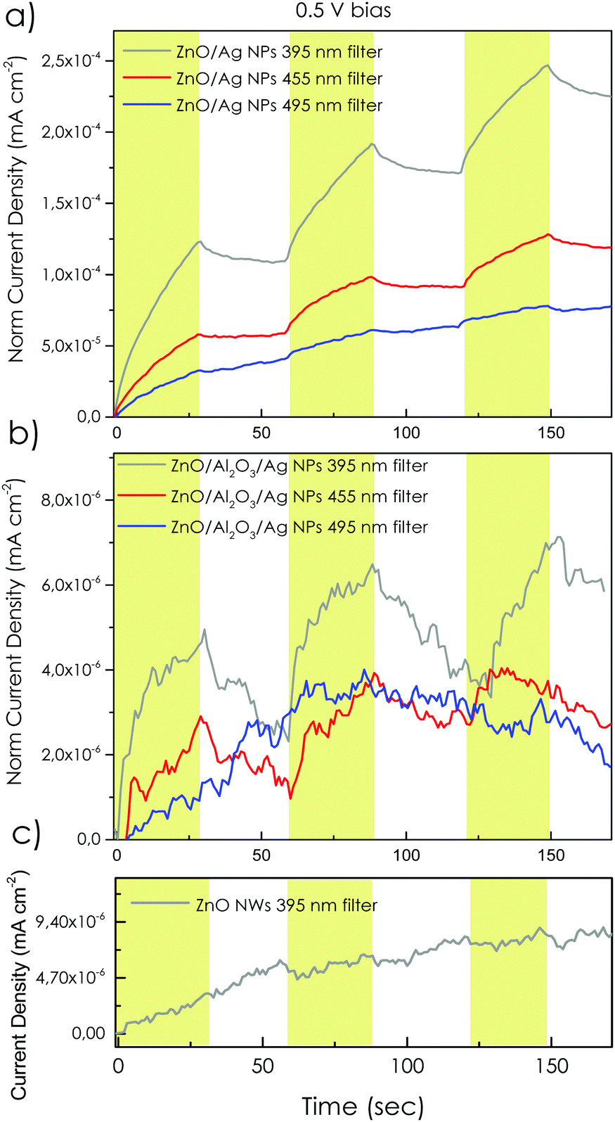 | ||
| Fig. 6 (a) and (b) Photoresponse of the samples at different optically filtered pulsed illuminations (395, 455 and 495 nm optical filters coupled with high-power LED with color temperature 5700 K with power density equivalent to simulated solar light AM 1.5 G) at 0.5 V applied potential. Yellow bands correspond to the illumination intervals. | ||
The overall photoresponse of the bare ZnO NRs under 0.5 V forward bias and unfiltered solar light irradiation (range 300 to 1200 nm) is shown in Fig. S7 (ESI†). Fig. 6(a) and (b) report the electrical response of Ag NPs decorated samples under filtered solar light irradiation (using 395, 455 and 495 nm long pass filters, which allow the light going through and reach the samples in the range of 400–850, 465–850 and 515–850 nm, respectively) under 0.5 V direct bias. The results were compared with the response of the bare ZnO NRs sample upon exposure to λ > 395 nm light (Fig. 6(c)). As expected, the undecorated sample (bare ZnO NRs), does not exhibit any peculiar response when exposed to λ > 395 nm white light, in agreement with the ZnO absorption edge. Remarkably, ZnO NRs/Ag NPs sample presented a pronounced current response to the 395 nm filtered light. The obtained photocurrent response of ZnO NRs/Ag NPs sample to λ > 395 filtered light in this case, presented an average derived current of about ∼15% of the bare unfiltered ZnO NRs (Fig. S7, ESI†). In addition, by increasing the optical filtering of the irradiated light from 395 to 495 nm the photocurrent response of the ZnO NR/Ag NP sample is gradually tapered off, in accordance with the absorption profile of the Ag NPs (Fig. 2(a)). The comparison with bare ZnO NRs sample suggests that light-induced photocurrent in ZnO NR/Ag NP samples is uniquely induced by the presence of the Ag NPs. In this regard, it can be deduced that the plasmonic electron–electron decay of excited Ag NPs could be transferred to the conduction band or the deep trap states of ZnO via combinatorial electron injection processes of direct hot electron transfer and dipole–dipole coupling. The samples with the Al2O3 passivating layer (ZnO NRs/Al2O3/Ag NPs), did result in non-negligible photoresponse upon illumination with λ > 395 nm. The current response of the sample ZnO NRs/Al2O3/Ag NPs is much smaller (∼67%) than the sample without spacer layer under the λ > 395 nm light irradiation (Fig. 6(b)) which again points towards a predominant DET mechanism.
In addition to the lower current intensity in the ZnO/Al2O3/Ag NP sample, the current decrease is also sharper, with respect to ZnO NRs/Ag NPs, when filtered light is applied. Current response is highly reduced when the energy of incident photon is reduced to λ > 455 nm and is completely turned off when photon energy is reduced to λ > 495 nm. The photoresponse of the ZnO/Al2O3/Ag NP sample in this case remarkably concurs with the obtained EQE profile of the sample. Hence we assume that the photoresponse of the samples with Al2O3 spacer layer can encompass the charge transfer mechanism from Ag NPs to ZnO through PIRET induction of the near-field enhancement and Fowler–Nordheim tunnelling-induced charge transfer processes.49,50
Conclusions
In conclusion, we investigated the photo-physics and the optoelectronic behavior of a hot-electron plasmonic Schottky system based on Ag NPs and ZnO NRs, with prospect of efficient light-harvesting suitable for photoconversion systems. We focused on the two dominant non-radiative plasmonic carrier transfer mechanisms: DET and PIRET processes. Overall, our findings in distinguishing the PIRET and DET processes can establish a new paradigm in light harvesting systems and designing optoelectronic devices. Specifically, we can anticipate that the studied PIRET mechanism in this work can be regarded as a valuable suggestion for the design of the devices with collective near-field enhancement possibilities. The comparison over the ZnO NRs decorated with Ag NPs, and analogous sample with an insulating layer, outlined the role of PIRET and its effect on increasing the population in a spectral region, where the semiconductor absorbs weakly. Our results indicated that the DET process can be a suitable method for sunlight harvesting in conversion devices through significant hot-carrier injection processes, if design consideration for the device architecture is the target. We found the time scale of photo-excited evolution, which includes electron redistribution from ZnO to Ag in less than 1 ps and the subsequent drop in the trap states in less than 2 ps, designated to the DET and PIRET process due to LSPR excitation of the NPs. We also demonstrated the non-radiative optical field coupling mechanism of Ag NPs with ZnO, with hot-electron injection, which results in a decrease in total ZnO emission. The results later highlighted the role of the Ag plasmonic response to non-radiative decay processes in ZnO, using two-state trapping model. Simultaneously, we demonstrated the optical field coupling mechanism of Ag NPs by the decreases in the total QY of ZnO emission, which further confirms the probability of non-radiative hot-electron injection involved in the LSPR decay of Ag NPs towards ZnO NRs. Finally, we found an increased photocurrent for the plasmon coupled samples. Overall, we could evidence and distinguish the role of DET and of PIRET in the non-radiative transfer processes. Our 1D architecture, intended for enhanced carrier collection, can reasonably favor the non-radiative carrier injection/transport of plasmonic damping, making the device promising for light conversion systems. It is noteworthy, these results can be applied to different metal plasmonic/semiconductors systems.Experimental methods
The ZnO NR arrays were synthesized via a hydrothermal method. Firstly, a seed layer was prepared by spin-coating of 1 × 10⁻² M zinc acetate dihydrate [Zn(CH3COO)2·2H2O] (Sigma-Aldrich) in ethanol solution on a fluorine-doped tin oxide (FTO) glass (Pilkinton TEC 15) substrate. The seeded FTO substrate was then calcinated in a furnace in an ambient atmosphere at 450 °C for 1 hour to assure complete oxidization of the spin coated layer. The hydrothermal reaction was started by immersing the seeded substrates in an aqueous solution of 1 × 10⁻² M zinc nitrate [Zn(NO3)2] (Sigma-Aldrich) and 1 × 10⁻² M of hexamethylene tetraamine (Sigma-Aldrich) inside a Teflon lined autoclave at 95 °C for 3 hours to perform the growth of ZnO NRs.Synthesis of the Ag NPs was carried out by reducing silver nitrate (AgNO3, Sigma-Aldrich), via the polyol method. A solution of 1 × 10⁻³ M polyvinylpyrrolidone (PVP, Mw = 104 g mol−1) and 1 × 10⁻² M AgNO3 in 20 mL ethylene glycol was prepared. Subsequently, the reaction took place in a Flexi Wave SK-1 microwave (MW) oven at 500 W for 40 s of MW radiation and the reaction temperature was increased to 120 °C. PVP serves as a capping agent, to promote nucleation and prevent the aggregation of the nanoparticles. Thereby, the silver nanoparticles were colloidally stabilized by the hydrocarbon chains of PVP polymer, possibly creating a micelle structure of silver capped with PVP molecules. Finally, the Ag NPs were washed with acetone and dispersed in ethanol for further sample preparation steps. Al2O3 insulating layer was deposited on the ZnO NRs by means of Atomic Layer Deposition (ALD), Savannah Cambridge nanotech. The deposition was carried out at 150 °C using repeated cycles of the trimethylaluminium precursor and deionized water. Ag NPs were uptaken on the as-prepared ZnO NRs via galvanostatic electrophoretic deposition (EPD). The electrophoretic deposition of the Ag NPs provides a comprehensive method for controlling the concentration of Ag NPs uptake. The amount of deposited Ag NPs was controlled by UV-vis spectroscopy of the EPD electrolyte in different deposition duration intervals using Beer–Lambert equation. It is estimated that overall ∼4.5 × 10⁻⁹ mol mm−2 of Ag NPs were deposited on ZnO NRs. The oxidation of the Ag NPs was prevented by applying low bias potentials (−0.5 V) during the EPD process and the micelle structure of NPs.
The morphology of the as-prepared bare ZnO NRs and ZnO NRs/Ag were characterized using a Magellan 400 Field emission scanning electron microscope (FE-SEM from FEI). The absorbance and diffuse reflectance spectra were recorded with Cary5000 UV-vis-NIR spectrophotometer. The X-ray diffraction pattern of the samples were carried out using PANalytical Empyrean diffractometer, Cu anode (kα1 emission line at 8.04 keV) scanning in the range of 15° < 2θ < 80°. Photoresponses of the samples were recorded using a spring-legged probe in local contact with the ZnO NR surface and another contact channeled to the FTO substrate. The samples are under controlled exposure of simulated solar light (1.5 AM), which can be screened by optical bandpass filters, thereby only permitting through specified range of the light. To avoid contribution of short circuit and shadowing effects, all electrical measurements were conducted without any deposited conductive electrical contacts, only using the spring-legged probe connected to the surface of samples (circular with 0.6 mm diameter). The optical range of the filters was explicitly mentioned in the results and discussions. EQE measurements were performed by illuminating the samples via a Newport Cornerstone260 light source equipped using a monochromatic light modulator with a 5 Hz chopper. Subsequently, the photo-generated current measured using a Keithley 2400 Lock-In amplifier. Rutherford backscattering spectrometry (RBS) was carried out by using a 1.8 MeV 4He+ ion beam, scattering angle θ = 160°, IBM geometry. The XRUMP code simulation was used for data analysis.
Steady state and transient photoluminescence were recorded using FLS980 high-resolution spectrometer, Edinburgh Instruments. A 372 nm pulsed diode laser (PDL) was used for excitation during the measurement of the lifetime of ZnO emission. Pump–probe experiments were carried out using a commercial Ti:Sapphire amplified laser system (Coherent Libra) delivering <100 fs pulses with a repetition rate of 1 kHz, carrier wavelength of 800 nm and average power of 4 W. Pump pulses at 266 nm were obtained using a homemade third harmonic generation setup. After generation, the residual second harmonic and fundamental wavelength were removed from the pump spectrum by a series of three dichroic mirrors having high reflectivity at 266 nm. The white light probe beam is generated by focusing a small power fraction of the fundamental beam into a 2 mm CaF2 plate and filtering out the residual fundamental with a BG39 filter. Synchronization between pump and probe pulses is obtained with a motorized translation stage. The pump and the probe are then focused on the sample by means of a CaF2 lens and an enhanced aluminum spherical mirror, respectively. The intensity of the pump beam is modulated at 0.5 kHz with a mechanical chopper. After the interaction between the probe and the excited sample, a fast optical multichannel analyzer working at the full repetition rate of the laser records the differential transmission ΔT/T = (TON − TOFF)/TOFF over the whole white light continuum as a function of the pump–probe delay. Here, TON and TOFF are the probe transmissions through the sample pump excited and unperturbed sample. The resolution limit of our setup is ∼100 fs and the incident pump fluence was set at ∼95 μJ cm−2.
Author contributions
MGK, SY and AC have contributed equally and majorly to this work. MGK performed the major part on sample preparation, conceptualization, formal analysis and writing the original draft. MZR and AC performed the transient absorption and validation of the results. AV, MZR and IC played a major role in validation, supervision and editing.Conflicts of interest
There are no conflicts to declare by the authors.Acknowledgements
The authors acknowledge the Swedish Foundations Consolidator Fellowship, the Luleå University of Technology Lab Fund program, the Kempe Foundation, the European Union Horizon 2020 research and innovation program (No. 654002) and the Knut & Alice Wallenberg Foundation. I. C. acknowledges VINNOVA under the VINNMER Marie Curie grant project Light energy, Li En, 2015.Notes and references
- A. Ziashahabi, M. Prato, Z. Dang, R. Poursalehi and N. Naseri, Sci. Rep., 2019, 9, 11839 CrossRef PubMed.
- R. Haldavnekar, K. Venkatakrishnan and B. Tan, Nat. Commun., 2018, 9, 1–18 CrossRef CAS PubMed.
- P. Nbelayim, G. Kawamura, W. Kian Tan, H. Muto and A. Matsuda, Sci. Rep., 2017, 7, 1–12 CrossRef CAS PubMed.
- J. Lehmann, M. Merschdorf, W. Pfeiffer, A. Thon, S. Voll and G. Gerber, Phys. Rev. Lett., 2000, 85, 2921–2924 CrossRef CAS PubMed.
- H. Hövel, S. Fritz, A. Hilger, U. Kreibig and M. Vollmer, Phys. Rev. B: Condens. Matter Mater. Phys., 1993, 48, 18178–18188 CrossRef PubMed.
- A. Furube and S. Hashimoto, NPG Asia Mater., 2017, 9, e454 CrossRef CAS.
- J. Wang, B. Li, T. Gu, T. Ming, J. Wang, P. Wang and J. C. Yu, ACS Nano, 2014, 8, 8152–8162 CrossRef PubMed.
- A. Manjavacas, J. G. Liu, V. Kulkarni and P. Nordlander, ACS Nano, 2014, 8, 7630–7638 CrossRef CAS.
- A. Camellini, A. Mazzanti, C. Mennucci, C. Martella, A. Lamperti, A. Molle, F. Buatier de Mongeot, G. Della Valle and M. Zavelani-Rossi, Adv. Opt. Mater., 2020, 8, 2000653 CrossRef CAS.
- S. K. Cushing, J. Li, F. Meng, T. R. Senty, S. Suri, M. Zhi, M. Li, A. D. Bristow and N. Wu, J. Am. Chem. Soc., 2012, 134, 15033–15041 CrossRef CAS PubMed.
- K. L. Kelly, E. Coronado, L. L. Zhao and G. C. Schatz, J. Phys. Chem. B, 2003, 107, 668–677 CrossRef CAS.
- X. Ma, Y. Dai, L. Yu, Z. Lou, B. Huang and M.-H. Whangbo, J. Phys. Chem. C, 2014, 118, 12133–12140 CrossRef CAS.
- N. Serpone and A. V. Emeline, J. Phys. Chem. Lett., 2012, 3, 673–677 CrossRef CAS PubMed.
- C. Clavero, Nat. Photonics, 2014, 8, 95–103 CrossRef CAS.
- S. Linic, P. Christopher and D. B. Ingram, Nat. Mater., 2011, 10, 911–921 CrossRef CAS PubMed.
-
Ü. Özgür, Y. I. Alivov, C. Liu, A. Teke, M. A. Reshchikov, S. Doǧan, V. Avrutin, S. J. Cho and H. Mork
![[o with combining cedilla]](https://www.rsc.org/images/entities/char_006f_0327.gif) , J. Appl. Phys., 2005;98:1–103 Search PubMed.
, J. Appl. Phys., 2005;98:1–103 Search PubMed. - S. Pearton, Springer Ser. Mater. Sci., 2012, 156, 14–15 Search PubMed.
- E. Comini, C. Baratto, G. Faglia, M. Ferroni, A. Vomiero and G. Sberveglieri, Prog. Mater. Sci., 2009, 54, 1–67 CrossRef CAS.
- P. Ghamgosar, F. Rigoni, M. G. Kohan, S. You, E. A. Morales, R. Mazzaro, V. Morandi, N. Almqvist, I. Concina and A. Vomiero, ACS Appl. Mater. Interfaces, 2019, 11, 23454–23462, DOI:10.1021/acsami.9b04838.
- I. Concina, Z. H. Ibupoto and A. Vomiero, Adv. Energy Mater., 2017, 7, 1–29 Search PubMed.
- S. Baruah, M. A. Mahmood, M. Tay and Z. Myint, Beilstein J. Nanotechnol., 2010, 14–20 CrossRef CAS.
- C. Chen, H. He, Y. Lu, K. Wu and Z. Ye, ACS Appl. Mater. Interfaces, 2013, 5, 6354–6359 CrossRef CAS PubMed.
- J. Rodrigues, T. Holz, R. Fath Allah, D. Gonzalez, T. Ben, M. R. Correia, T. Monteiro and F. M. Costa, Sci. Rep., 2015, 5, 10783 CrossRef CAS.
- E. Muchuweni, T. S. Sathiaraj and H. Nyakotyo, Mater. Sci. Eng., B, 2018, 227, 68–73 CrossRef CAS.
- L. H. Quang, S. J. Chua, K. P. Loh and E. Fitzgerald, J. Cryst. Growth, 2006, 287, 157–161 CrossRef CAS.
- S. You, A. Patelli, P. Ghamgosar, T. Cesca, F. Enrichi, G. Mattei and A. Vomiero, APL Mater., 2019, 7, 081111 CrossRef.
- K. Zhang, Z. L. Wang and Y. Yang, ACS Nano, 2016, 10, 10331–10338 CrossRef CAS PubMed.
- N. Gogurla, A. K. Sinha, S. Santra, S. Manna and S. K. Ray, Sci. Rep., 2014, 4, 6483, DOI:10.1038/srep06483.
- Q.-H. Ren, Y. Zhang, H.-L. Lu, H.-Y. Chen, Y. Zhang, D.-H. Li, W.-J. Liu, S.-J. Ding, A.-Q. Jiang and D. W. Zhang, Nanotechnology, 2016, 27, 165705 CrossRef PubMed.
- K. Ueno, T. Oshikiri, Q. Sun, X. Shi and H. Misawa, Chem. Rev., 2018, 118, 2955–2993 CrossRef CAS.
- Y. Ohko, T. Tatsuma, T. Fujii, K. Naoi, C. Niwa, Y. Kubota and A. Fujishima, Nat. Mater., 2003, 2, 29–31 CrossRef CAS.
- T. Wang, Z. Jiao, T. Chen, Y. Li, W. Ren, S. Lin, G. Lu, J. Ye and Y. Bi, Nanoscale, 2013, 5, 7552–7557 RSC.
- X. D. Zhou, X. H. Xiao, J. X. Xu, G. X. Cai, F. Ren and C. Z. Jiang, EPL, 2011, 93, 0–6 CAS.
- J. Jadhav and S. Biswas, Ceram. Int., 2016, 42, 16598–16610 CrossRef CAS.
- F. P. García de Arquer, A. Mihi, D. Kufer and G. Konstantatos, ACS Nano, 2013, 7, 3581–3588 CrossRef PubMed.
- Y. Zheng, L. Zheng, Y. Zhan, X. Lin, Q. Zheng and K. Wei, Inorg. Chem., 2007, 46, 6980–6986 CrossRef CAS.
- H. R. Liu, G. X. Shao, J. F. Zhao, Z. X. Zhang, Y. Zhang, J. Liang, X. G. Liu, H. S. Jia and B. S. Xu, J. Phys. Chem. C, 2012, 116, 16182–16190 CrossRef CAS.
- A. Ziashahabi, M. Prato, Z. Dang, R. Poursalehi and N. Naseri, Sci. Rep., 2019, 9, 1–12 CAS.
- S. S.-U. Rahman, K. Sebald, J. Gutowski, T. Klein, S. Klembt, C. Kruse and D. Hommel, Phys. Status Solidi, 2016, 13, 498–502 CrossRef.
- H. Chen, G. Liu and L. Wang, Sci. Rep., 2015, 5, 10852 CrossRef CAS PubMed.
- J. Li, S. K. Cushing, F. Meng, T. R. Senty, A. D. Bristow and N. Wu, Nat. Photonics, 2015, 9, 601–607 CrossRef CAS.
- A. L. Efros, in Nanocrystal Quantum Dots, ed. V. I. Klimov, CRC Press, New York, 1st edn., 2003, pp. 97–132 Search PubMed.
- J. Z. Zhang, Acc. Chem. Res., 1997, 30, 423–429 CrossRef CAS.
- H. Weller, A. Eychmüller, R. Vogel, L. Katsikas, A. Hässelbarth and M. Giersig, Isr. J. Chem., 1993, 33, 107–113 CrossRef CAS.
- S. Acharya, S. Chouthe, H. Graener, T. Böntgen, C. Sturm, R. Schmidt-Grund, M. Grundmann and G. Seifert, J. Appl. Phys., 2014, 115, 053508 CrossRef.
- J.-Y. Bigot, V. Halté, J.-C. Merle and A. Daunois, Chem. Phys., 2000, 251, 181–203 CrossRef CAS.
- R. Sato, M. Ohnuma, K. Oyoshi and Y. Takeda, Phys. Rev. B: Condens. Matter Mater. Phys., 2014, 90, 125417 CrossRef.
- J. H. Hodak, I. Martini and G. V. Hartland, J. Phys. Chem. B, 1998, 102, 6958–6967 CrossRef CAS.
- X.-C. Ma, Y. Dai, L. Yu and B.-B. Huang, Light: Sci. Appl., 2016, 5, e16017 CrossRef CAS PubMed.
- W. P. Putnam, R. G. Hobbs, P. D. Keathley, K. K. Berggren and F. X. Kärtner, Nat. Phys., 2017, 13, 335–339 Search PubMed.
Footnotes |
| † Electronic supplementary information (ESI) available. See DOI: 10.1039/d1tc03032a |
| ‡ These authors contributed equally to the work. |
| This journal is © The Royal Society of Chemistry 2021 |