
 Open Access Article
 This Open Access Article is licensed under a Creative Commons Attribution-Non Commercial 3.0 Unported Licence
Ultrathin PTAA interlayer in conjunction with azulene derivatives for the fabrication of inverted perovskite solar cells†
Nikolaos
Tzoganakis‡
a,
Boxu
Feng‡
b,
Michalis
Loizos
a,
Miron
Krassas
a,
Dimitris
Tsikritzis
 ac,
Xiaodong
Zhuang
*b and
Emmanuel
Kymakis
*ac
ac,
Xiaodong
Zhuang
*b and
Emmanuel
Kymakis
*ac
aDepartment of Electrical & Computer Engineering, Hellenic Mediterranean University (HMU), Heraklion 71410, Crete, Greece. E-mail: kymakis@hmu.gr
bMeso-Entropy Matter lab, State Key Laboratory of Metal Matrix Composites Shangai Key Laboratory of Electrical Insulation and Thermal gaining, School of Chemistry and Chemical Engineering, Frontiers Science Center for Transformative Molecules, Shanghai Jiao Tong University, Shanghai 200240, P. R. China. E-mail: zhuang@sjtu.edu.cn
cInstitute of Emerging Technologies (i-EMERGE) of HMU Research Center, Heraklion 71410, Crete, Greece
First published on 17th September 2021
Abstract
Perovskite solar cells (PSCs) have reshaped thin-film photovoltaic technology owning to their exceptionally high power conversion efficiency (PCE) values in conjunction with their low-cost and facile production. PSCs are fabricated following either an inverted or a normal material stacking structure. Inverted PSCs, although they exhibit lower PCE values compared with normal PSCs, show negligible hysteresis, a better stability, and a prolonged lifetime. In this work, novel azulene derivatives, namely Az-4TPA and biAz-4TPA, were synthesized and incorporated in inverted PCEs. These new molecules were extensively characterized and showed good optoelectronic properties. Furthermore, we uncover the relationship between the PCE and the wetting properties of the substrate on which the perovskite layer is grown, demonstrating that a hydrophobic substrate is required. To increase the hydrophobicity of the azulene thin film's surface, PTAA was used. By forming an ultra-thin biAz-4TPA/PTAA bilayer, the optimized devices reached a PCE up to 18.48% and displayed an extended lifetime.
Introduction
Organic–inorganic hybrid perovskite solar cells (PSCs) have shown a remarkable evolution in terms of their power conversion efficiency (PCE), reaching 25.2%.1 Moreover, the layers of PSCs materials are mostly deposited from solutions2 and using techniques that are scalable for large-area devices with high throughput,3,4 and thus PSCs have the potential to dominate the market, either as standalone thin-film solar cells5 or as tandem solar cells with established silicon solar cells.6,7Two types of cell architecture dominate PSCs, that is, normal or inverted PSCs, that can have either a planar8 or a mesoporous structure.9 Currently, normal PSCs show the highest efficiencies and have been widely investigated; however, their major drawbacks are high hysteresis,10,11 short lifetimes due to the sensitive spiro-OMeTAD material,12,13 and high fabrication costs due to the Au top metal electrode.14 On the other hand, inverted PSCs are mostly hysteresis free,15 are more stable than normal PSCs16,17 and they use the cheaper Ag, Al or Cu as their back electrodes.18,19 However, inverted PSCs deliver lower PCE compared to normal PSCs, and expensive materials are used, such as [6,6]-phenyl-C61-butyric acid methyl ester (PCBM) and poly[bis(4-phenyl)(2,4,6-trimethylphenyl)amine] (PTAA).
Most high-performing inverted PSCs use PTAA as the hole-transport later (HTL) material20 due to its high conductivity and low absorption in the visible region.21,22 Furthermore, PTAA shows improved stability compared with spiro-OMeTAD, which it replaces when the lifetime is of importance for stable normal PSCs,23 and, most importantly, PTAA can easily be deposited from solution onto flexible24 and rigid substrates. However, the cost of PTAA and of PCBM,25 the most common electron-transport layer (ETL) material, is high,26 rendering inverted PSCs expensive and unfavorable for modules.27 PTAA outperforms most common inorganic and polymer HTLs such as NiOx28 and PEDOT:PSS,21,29 but it is UV sensitive,30 which limits the lifetime of the device. Therefore, alternative materials for PTAA are sought that are suitable for large-area and flexible substrates, i.e., they must be soluble in common solvents, have low-temperature annealing requirements and be of low cost for delivering high-PCE devices. Various oxides31–34 and organic materials35–40 have been developed as HTLs in PSCs instead of PTAA, but some of the most successful and high-performance approaches employ a bilayer of PTAA with another material. More specifically, a bilayer of PEDOT:PSS/PTAA increases the PCE from 16.94% up to 19%41 and to 19.41% on flexible substrates.42 Similarly, Du et al. have prepared a NiOx/PTAA bilayer that increased the PCE up to 17.1%.43 Moreover, PTAA bilayers have been formed in conjunction with reduced graphene oxide,44 graphene,45 CuOx,46 PFN-P2,47 NiOx,48 and VOx.49
In this work, two novel molecules, biAz-4TPA (4,4′,4′′,4′′′-([6,6′-biazulene]-1,1′,3,3′-tetrayl)tetrakis(N,N-diphenylaniline)) and Az-4TPA (4,4′,4′′,4′′′-(azulene-1,3,5,7-tetrayl)tetrakis(N,N-diphenylaniline)), were synthesized and incorporated in inverted PSCs as the HTL. Moreover, we develop an innovative approach of reducing the PTAA requirements in inverted PSCs by 62%. This is achieved by substituting the PTAA layer with a thin bilayer formed of biAz-4TPA and PTAA. PTAA was developed over the biAz-4TPA layer in order to increase the hydrophobicity of the surface, which is required for the satisfactory formation and crystallization of the perovskite layer. Using solutions only, we fabricated inverted PCEs with varying biAz-4TPA/PTAA film thicknesses. The devices incorporating the optimal biAz-4TPA/PTAA bilayer show a higher PCE, up to 18.48%, and an improved lifetime while reducing the requirements of expensive PTAA. Our approach greatly reduces the total mass requirements for the HTL from 2 mg to 1 mg. The results confirm that the azulene derivative biAz-4TPA facilitates hole extraction and that PTAA is an efficient surface-modification material for increasing the hydrophobicity of the substrate, allowing better formation of the perovskite film.
Experimental
The solvents and the commercial reagents were used as received, unless otherwise stated. The synthesis and characterization of the novel compounds are described in the ESI† (S12–S26).Material characterization
Atomic force microscopy (AFM) measurements were performed in air using XE7 AFM instrument (Park System, Korea). The images were acquired using a PPP-NCHR cantilever (Nanosensors, USA), which has a tip with a nominal diameter of 10 nm. Image acquisition was performed using a drive frequency of ∼295 kHz. Intermittent contact mode was used to record the image over an area of 10 × 10 μm (512 × 512 data points), using a scan rate of 0.7 Hz. The working set point was above 70% of the free oscillation amplitude. The raw AFM images were processed using the free Gwyddion software.50 An Ossila contact angle goniometer was used for the contact angle measurements. The UV-Vis spectra were acquired using a Shimadzu UV-2401 PC Recording Spectrophotometer. Steady-state photoluminescence and time-resolved photoluminescence measurements of the perovskite films were conducted using an FS5 spectrofluorometer (Edinburgh Instruments). A pulsed laser diode (λ = 478.4 nm, pulse full-width at half-maximum < 70 ps, and repetition rate 200 kHz–40 MHz) was used to excite the samples.Device fabrication
Pre-patterned glass/ITO substrates were cleaned using an ultrasonic bath with deionized water, acetone, and isopropanol (IPA), respectively, 15 min in each step. Then, the samples were transferred to an N2 glovebox, where they underwent UV-ozone treatment for 15 min. The biAz-4TPA solution was prepared by dissolving the synthesized powder in chloroform or chlorobenzene (Sigma Aldrich) achieving a concentration of 0.25 mg mL−1. Then 45 μL of the prepared solution was dynamically dispensed at 2000 rpm for 35 s onto the glass/ITO surface. Afterwards, an ultra-thin layer of PTAA (Solaris, Mw = 20–70 kDa) was prepared by spin coating from a PTAA solution in toluene with varying concentrations (2–0.1 mg mL−1), at an angular speed of 6000 rpm and for 30 s. The biAz-4TPA/PTAA films were annealed at 110 °C for 10 min. The perovskite solution was prepared by mixing 0.2 M MABr (GreatCell Solar), 1.14 M FAI (GreatCell Solar), 0.2 M PbBr2 (Alfa Aesar) and 1.24 M PbI2 (TCI America) in 4![[thin space (1/6-em)]](https://www.rsc.org/images/entities/char_2009.gif) :1 v/v anhydrous dimethylformamide (DMF) (99.8%, Sigma Aldrich):dimethyl sulfoxide (DMSO) (99.9%, Sigma Aldrich) and then adding 5 vol% from a 1.5 M CsI (Alfa Aesar) stock solution and 4 vol% from a 1.5 M RbI (Alfa Aesar) stock solution. The perovskite layers were dynamically spin coated onto the biAz-4TPA/PTAA film at 6000 rpm for 45 s. 20 s prior to the end of the spinning process, 200 mL of anhydrous chlorobenzene (CB) (99.8%, Sigma Aldrich) was dropped onto the spinning perovskite film. Subsequently, the samples were immediately annealed for 45 min on a preheated hotplate at 100 °C. Next, a thin layer of PC60BM (99%, Solenne) approximately 30 nm thick, was deposited by spin coating a 20 mg mL−1 PC60BM solution in anhydrous CB onto the perovskite at 2000 rpm for 60 s. Afterwards, 45 μL from a 0.5 mg mL−1 bathocuproine (BCP) solution (96%, Sigma Aldrich) prepared in IPA (99.5% extra dry, ACROS Organics) was dispersed and spin coated onto the PC60BM at 4000 rpm for 45 s. Finally, a 100-nm-thick Ag top electrode was deposited by thermal evaporation under a high vacuum of 10−6 mbar.
:1 v/v anhydrous dimethylformamide (DMF) (99.8%, Sigma Aldrich):dimethyl sulfoxide (DMSO) (99.9%, Sigma Aldrich) and then adding 5 vol% from a 1.5 M CsI (Alfa Aesar) stock solution and 4 vol% from a 1.5 M RbI (Alfa Aesar) stock solution. The perovskite layers were dynamically spin coated onto the biAz-4TPA/PTAA film at 6000 rpm for 45 s. 20 s prior to the end of the spinning process, 200 mL of anhydrous chlorobenzene (CB) (99.8%, Sigma Aldrich) was dropped onto the spinning perovskite film. Subsequently, the samples were immediately annealed for 45 min on a preheated hotplate at 100 °C. Next, a thin layer of PC60BM (99%, Solenne) approximately 30 nm thick, was deposited by spin coating a 20 mg mL−1 PC60BM solution in anhydrous CB onto the perovskite at 2000 rpm for 60 s. Afterwards, 45 μL from a 0.5 mg mL−1 bathocuproine (BCP) solution (96%, Sigma Aldrich) prepared in IPA (99.5% extra dry, ACROS Organics) was dispersed and spin coated onto the PC60BM at 4000 rpm for 45 s. Finally, a 100-nm-thick Ag top electrode was deposited by thermal evaporation under a high vacuum of 10−6 mbar.
Device characterization
The PSCs were evaluated under an inert atmosphere using an ABB solar simulator (Sol1A, Oriel), equipped with a 450 W Xe lamp and an AM1.5G filter. The intensity was calibrated at 100 mW cm−2 using a KG3-window Si reference cell. The J–V curves were recorded at a constant scan rate of 20 mV s−1 using a multiplexor test board system (Ossila), and no device preconditioning was applied before the measurements. A black metallic aperture mask was used during each measurement to set the active area of the fabricated devices at 0.04 cm2 and to reduce the influence of the scattered light. The external quantum efficiency (EQE) spectra were recorded using a QE-T system from Enlitech. A chopping frequency of 60 Hz was used. Calibration of the light intensity was performed using a quartz-window Si solar cell. The integrated current density was calculated by integrating the product between the spectral response of the test cell and the AM1.5G reference spectrum. Optoelectrical characterization was performed using a transient module of a commercially available measurement platform, ARKEO (Cicci Research s.r.l.). Transient photovoltage (TPV) experiments were performed in small perturbation mode by confining the intensity of the light pulse to less than 10% of the background voltage. Thus, the equilibrium of the field induced by the background bias remained undisturbed. By doing so, the voltage decay of the measured devices follows first-order behavior and directly reflects the lifetime of the charge carriers. Transient photocurrent (TPC) experiments were performed in both large and small perturbation regimes. Large perturbations were induced over 200 ms under a 0.8 duty cycle, while small perturbations were loaded with a 0.001 cycle and passed through an external circuit of 50 Ω resistance. Signals from both the open-circuit voltage (for TPV) and the short-circuit current (for TPC) were monitored after passing them through voltage and impedance amplifiers, respectively. In order to observe the photoinduced charge extraction through linearly increasing voltage (photo-CELIV) measurements, a 470 nm fast LED source driven by a 100 mA current and exhibiting a Lambertian radiation pattern was used. The relaxation pulse width was set to 20 ms, charged by a 50000 V s−1 ramp, following a 13 ms delay after the injection pulse. The collected signals were processed through a transimpedance amplifier and passed through a 100 MHz bandwidth digitizer running in single-shot mode. The lifetime behavior of the PSCs was monitored using an ISOS testing laboratory from InfinityPV in ISOS-L2 operation mode. The devices were first encapsulated with a piece of glass and a UV-curable epoxy as an adhesive (Ossila E132). Then, the devices were placed inside the test chamber and exposed under continuous illumination. The apparatus was equipped with a solar simulator using a metal halide light source simulating the AM1.5G spectrum in the range of 300–900 nm. The light intensity was calibrated at 100 mW cm−2 using a Si reference cell. The humidity in the test chamber was below 15%, while the temperature was over 65 °C. Between the J–V measurements the devices were left in the open-circuit condition.
Results and discussion
Fig. 1a shows the molecular structures of the novel azulene derivatives, namely Az-4TPA and biAz-4TPA. Az-4TPA was prepared through Suzuki coupling between Az-4Bpin and 4-bromo-N,N-diphenylaniline; biAz-4TPA was prepared through Suzuki coupling between 4Br-Bi-Az and (4-(diphenylamino)phenyl)boronic acid (synthetic details and characterizations are provided in the ESI†). The electrochemical properties of both molecules were explored using cyclic voltammetry (CV) under an argon atmosphere in dichloromethane (DCM) solution with 0.1 M NBu4PF6 at a scan rate of 20 mV s−1. CV exhibited an electron oxidation wave with an anodic peak potential Epa1 at 0.49 and 0.67 V vs. Fc/Fc+ for Az-4TPA and biAz-4TPA, respectively, assigned to the one-electron oxidation of the lateral TPA branch (Fig. 1b). From CV measurement, the highest occupied molecular (HOMO) energy levels of Az-4TPA and biAz-4TPA are −4.83 and −5.01 eV using the equation of EHOMO = [(EOX − E1/2(Ferrocene)) + 4.8] eV (Fc+/Fc (−4.8 eV) as a reference), respectively. The photo-physical properties of Az-4TPA and biAz-4TPA were characterized via UV-Vis absorption and PL measurements in the solution state at room temperature. In Fig. 1c, the UV-Vis absorption spectra, in chloroform solution, showed an intense absorption mainly in the UV region because of the limited conjugation length in each molecule, which was deliberately designed to be transparent in the visible region, and the absorption maximum (λabsmax) was at 310 nm for Az-4TPA and 352 nm for biAz-4TPA, and the onset point (λabsonset) was at 507 nm for Az-4TPA and 457 nm for biAz-4TPA (Fig. S1, ESI†). From the absorption onsets, the optical band gaps were estimated to be 2.44 and 2.71 eV for Az-4TPA and biAz-4TPA, respectively. The different optical band gaps of Az-4TPA and biAz-4TPA can be attributed to their different degrees of electronic conjugation in the molecule. The azulene moiety of Az-4TPA can make the molecule more conjugated, while the 6,6′-biazulenyl moiety of biAz-4TPA has a repulsion effect between the hydrogens on the two seven-membered rings, resulting in the lower conjugation of biAz-4TPA. Meanwhile, upon excitation (378 nm) of Az-4TPA and biAz-4TPA, intense emissions at around 410, 434 and 460 nm were observed (Fig. 1c). To corroborate their HOMO energy levels, we also performed ultraviolet photoelectron spectroscopy (UPS) measurements (Fig. 1d and Fig. S2, ESI†). The ionization potential (IP) values were determined according to the equation IP = hν − (Ecutoff − EH, onset) to be 4.82 and 4.77 eV for Az-4TPA and biAz-4TPA, respectively. Combining the measured IP and the optical bandgap values, the LUMO levels of Az-4TPA and biAz-4TPA were estimated to be −2.38 and −2.06 eV, respectively. These frontier orbital energy levels calculated via UPS are more practical than those from CV due to the use of solid-state measurements. In Table S1 (ESI†) are listed the estimated values for the band gap, the HOMO and the LUMO for both materials. In Fig. 2 we compare the estimated energy levels of the new azulene derivatives with that of PTAA and perovskite. The suitable optical band gap and the perfect match of the energy levels of Az-4TPA and biAz-4TPA with PTAA suggest that these two small molecules might be excellent HTL candidates in perovskite solar cells. | ||
| Fig. 1 (a) Chemical structures of Az-4TPA and biAz-4TPA. (b) Cyclic voltammetry curves of Az-4TPA and biAz-4TPA in dichloromethane with 0.1 M NBu4PF6 at a scan rate of 20 mV s−1. (c) UV-Vis absorption spectra of Az-4TPA (1 × 10⁻⁸ mol L−1) and biAz-4TPA (5 × 10⁻⁹ mol L−1), and steady-state fluorescence spectra of Az-4TPA (1 × 10⁻⁵ mol L−1) and biAz-4TPA (5 × 10⁻⁵ mol L−1) in chloroform (both excitations at 378 nm). (d) Ultraviolet photoelectron spectroscopy (UPS) spectra of biAz-4TPA. | ||
 | ||
| Fig. 2 Energy level diagram of Az-TPA, biAz-4TPA and perovskite materials. The values are referenced to the vacuum energy Ev, which is assumed to be 0 eV. The dashed lines indicate the Fermi level. The LUMO and HOMO of PTAA were set at 2.3 and 5.2 eV, respectively. For the perovskite, the conduction band (CB) was set at 3.9 eV and the valance band (VB) at 5.4 eV. | ||
The solubilities of the Az-4TPA and biAz-4TPA molecules were tested in various solvents in order to select the most appropriate solvent for the spin-coating process and to estimate their maximum solubility. Fig. S3 (ESI†) shows solutions of 1 mg of Az-4TPA and biAz-4TPA in 1 mL of chlorobenzene, DMF, dichloromethane and chloroform. Both materials have a low solubility in DMF and chlorobenzene, but a high solubility in chloroform. Az-4TPA shows low solubility in dichloromethane, while biAz-4TPA is soluble in this solvent. Therefore, chloroform is an excellent solvent for both materials. However, chloroform is highly toxic, very reactive and a low-boiling solvent that should be avoided if possible. Therefore, the materials were dissolved in hot chlorobenzene instead, since it is a safer solvent and is extensively used in the fabrication of perovskite solar cells. 20 mg of biAz-4TPA is soluble in 1 ml chlorobenzene at 120 °C (Fig. S3i, ESI†).
Thin films of Az-4TPA and biAz-4TPA were deposited on ITO from a 1 mg mL−1 solution and they were characterized in terms of their morphology and optoelectronic properties. The morphology of the Az-4TPA and biAz-4TPA films was studied using AFM. The thin films showed an excellent morphology according to the optical microscopy images and AFM topography images presented in Fig. S4 (ESI†). The resulting thin films are very smooth and show an RMS roughness of about 1 nm. Similarly, biAz-4TPA forms a very smooth and compact thin film on ITO with an RMS roughness of 1.4 nm.
The hydrophilicity of the surface of the thin film is a critical parameter that controls the wettability and the growth of the overlayers. Thus, in addition to surface morphology characterization using AFM, the thin films of Az-4TPA and biAz-4TPA were characterized via contact angle measurements. These measurements involve a sessile water droplet on the test surface while monitoring the evolution of the droplet. The wettability of the surface is revealed by the resulting contact angle, and if the contact angle is high, i.e., close to 90°, then the surface is considered to be hydrophobic. Fig. 3 compares the contact angle of the water droplet formed on thin films of (a) biAz-4TPA formed from 1 mg mL−1 solution, (b) biAz-4TPA (0.25 mg mL−1)/PTAA(0.75 mg mL−1), (c) Az-4TPA formed from 1 mg mL−1 solution and (d) pure PTAA formed from 2 mg mL−1 solution. The azulene derivatives show high hydrophilicity since the contact angle was measured at ∼48.8° and 49.5° for biAz-4TPA and Az-4TPA, respectively. By contrast, the biAz-4TPA/PTAA and pure PTAA surfaces are considered to be hydrophobic with contact angles of 78.9° and 82.5°, respectively. PTAA is highly hydrophobic, which facilitates the growth of high-quality perovskite polycrystalline thin films.51
 | ||
| Fig. 3 Water contact angle measurements of (a) biAz-4TPA, (b) optimal biAz-4TPA/PTAA bilayer, (c) Az-4TPA and (d) PTAA (2 mg mL−1). The azulene thin films show hydrophilicity, exhibiting contact angles of 48.8° and 49.5° for (a) biAz-4TPA and (c) Az-4TPA, respectively. The hydrophobicity increases with the PTAA interlayer. Pure PTAA in panel (d) shows a contact angle of 80.8°. The contact angle of the biAz-4TPA/PTAA bilayer in panel (b) was measured at 78.9°. | ||
Finally, in order to fully characterize the materials regarding their optoelectronic properties, we measured the conductivity of the thin films using the two-probe method. Specifically, a thin film of known thickness was sandwiched between ITO and an evaporated Au metal electrode. Using a Keithley source measurement unit, the current density response was measured by varying the voltage from −2 V to 2 V. Fig. S5a (ESI†) shows the current density versus the applied voltage. The experimental points fall in a straight line for both materials, indicating ohmic behaviour and similar conductivities. From the slope of the line, we estimate the conductivity to be ∼2.05 × 10⁻⁵ S cm−1 for both materials.
The newly synthesized organic molecules were first tested as PTAA replacement in order to probe the charge-extraction dynamics of the new materials in the PSCs. Fig. S6 (ESI†) compares the performance of the control devices and devices incorporating biAz-4TPA or Az-4TPA as HTLs. The devices employing the azulene derivatives deliver a low PCE, which is around 10%. The performance of Az-4TPA is systematically lower compared with biAz-4TPA. Hence, we focused on biAz-4TPA for further development. We varied the concentration of the biAz-4TPA solution in order to tune the thickness of the HTL in the fabricated devices. This optimization procedure revealed the optimum concentration of the biAz-4TPA solution to be 0.25 mg mL−1. To investigate the reason for the low PCE in biAz-4TPA-only devices, we deposited thin films of biAz-4TPA, PTAA and a bilayer of biAz-4TPA/PTAA on ITO, followed by a perovskite layer. The samples were investigated in terms of the morphology and dynamics of the carriers. The surface of the samples was characterized via AFM and the topography images are presented in Fig. 4 and compared with the perovskite layer grown on PTAA, which is the control sample. Clearly, the surface morphology of the perovskite is affected by the substrate. Compared with the perovskite grown on PTAA, the perovskite grown on biAz-4TPA shows grains that are not well formed and the thickness of the perovskite layer is lower. On the other hand, crystallization of the perovskite layer grown on biAz-4TPA is not altered according to the XRD diffractograms of Fig. S7 (ESI†) and UV-Vis absorption measurements (Fig. S5b, ESI†). We conclude that the biAz-4TPA substate due to its lower hydrophobicity, compared to PTAA, negatively affected the growth of the perovskite layer, decreasing the performance of the devices. To resolve this, we increased the hydrophobicity of the biAz-4TPA surface by using the hydrophobic PTAA over biAz-4TPA, forming an ultra-thin bilayer of biAz-4TPA/PTAA. The thickness of PTAA was reduced as a result of using lower concentrations of PTAA solutions. The goal was to uncover the minimum amount of PTAA need to form an ultrathin layer over biAz-4TPA, which is enough to increase the hydrophobicity of the surface and to form a good perovskite layer, but without hindering the charge extraction. Fig. 4c reveals that the morphology of the perovskite layer deposited on biAz-4TPA/PTAA is similar to the control device. Moreover, PL analysis, as shown in Fig. 5a, reveals that the biAz-4TPA/perovskite interface facilitates charge extraction, while the bilayer with PTAA shows more quenching indicating improved charge extraction. Reducing the thickness of the PTAA layer further increases the PL quenching. Transient PL analysis agrees with the improved charge extraction at the biAz-4TPA/PTAA interface. Fig. 5b shows the transient PL curves of the biAz-4TPA/perovskite and biAz-4TPA/PTAA/perovskite interfaces, demonstrating the improved interface of biAz-4TPA with an ultra-thin PTAA layer on top. However, the PL decay shows similar results for all the samples, which indicates that biAz-4TPA exhibits a comparable performance to PTAA in terms of hole transfer, and devices without the PTAA interlayer show a worse performance due to the not well-formed perovskite morphology that is induced by the low hydrophobicity of biAz-4TPA. Consequently, biAz-4TPA can efficiently extract hole carriers, but interface engineering is needed to increase the hydrophobicity of the surface. This is achieved by the ultra-thin film of PTAA over the biAz-4TPA surface.
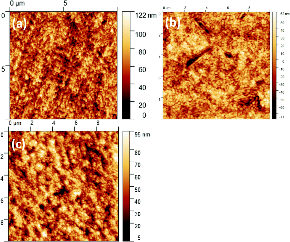 | ||
| Fig. 4 AFM images of the perovskite layer grown on (a) biAz-4TPA, (b) PTAA and (c) the optimal biAz-4TPA/PTAA bilayer. | ||
 | ||
| Fig. 5 Steady-state (a) and transient photoluminescence (b) characterization of the perovskite deposited on biAz-4TPA, the biAz-4TPA/PTAA bilayer and on glass. | ||
The performance of the devices was monitored via current–voltage measurements under 1 Sun conditions. Fig. 6 presents the optimized results on varying the PTAA interlayer thickness. For clarity in the figures, we use the shorthand ‘biAz’ instead of the complete name biAz-4TPA. Without reducing the PTAA thickness and by inserting the biAz-4TPA layer in the control device (biAz/PTAA, 2 mg mL−1), the PCE does not decline, which signifies the good charge extraction of biAz-4TPA and the favourable energy level alignment. This agrees with the energy level diagram of Fig. 2 and confirming that the biAz-4TPA/PTAA bilayer extracts holes efficiently. The hydrophobicity of PTAA is a crucial parameter that controls the PCE of the devices; thus, in order to obtain working devices we only need to have a very thin bilayer of biAz-4TPA/PTAA. In this context, we decreased the PTAA concentration, i.e., we reduced the PTAA thickness. The PCE shows a slight improvement with reducing the PTAA thickness, as is shown in Fig. 6 and Table 1. Table 1 summarizes the photovoltaic parameters, i.e., the short-circuit current (Jsc), the open-circuit voltage (Voc), the fill factor (FF), and the PCE, extracted from the current–voltage curves (Fig. S8, ESI†). Further decreasing the PTAA thickness results in a steady increase of the PCE up to the PTAA concentration of 0.75 mg mL−1, which is the optimal value, delivering a mean PCE of 17.42% and a champion cell of 18.48%. The improvement derives from the higher Voc, FF and Jsc upon formation of the optimal biAz-4TPA/PTAA bilayer. This behaviour concurs with the PL characterization results, which showed improved charge extraction within the optimal biAz-4TPA/PTAA (0.75 mg mL−1) bilayer. Lower concentrations result in a non-uniform PTAA interlayer, which was manifested by the lower FF, Voc and Jsc values obtained. Moreover, Fig. 6 correlates the contact angle values with the PCE. Hydrophobic surfaces, which are the case for a PTAA concentration of more than 0.5 mg mL−1, deliver high PCE values, whereas we observe a significant drop in the PCE when the biAz-4TPA/PTAA surface becomes hydrophilic at a PTAA concentration below 0.25 mg mL−1.
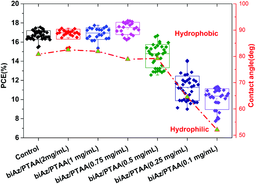 | ||
| Fig. 6 Box chart of the photovoltaic performance of the control device compared with the PSCs that incorporate the biAz-4TPA/PTAA interlayer with a decreasing PTAA film thickness. The triangle symbols indicate the contact angle values for each surface. Lower contact angles translate to a hydrophilic surface. The contact angle values were extracted from the images in Fig. S9 (ESI†). | ||
| PSC | PCE (%) | J sc (mA cm−2) | V oc (V) | FF (%) |
|---|---|---|---|---|
| Control | 16.72 ± 0.47 (17.49) | 20.12 ± 0.36 (21.30) | 1.099 ± 0.010 (1.111) | 74.52 ± 1.61 (73.92) |
| biAz/PTAA (2 mg mL−1) | 16.82 ± 0.53 (17.72) | 20.69 ± 0.26 (21.26) | 1.097 ± 0.013 (1.093) | 74.09 ± 1.99 (76.29) |
| biAz/PTAA (1 mg mL−1) | 16.88 ± 0.61 (17.81) | 20.41 ± 0.50 (21.11) | 1.106 ± 0.017 (1.103) | 74.77 ± 1.84 (76.49) |
| biAz/PTAA (0.75 mg mL−1) | 17.42 ± 0.64 (18.48) | 20.81 ± 0.40 (21.87) | 1.105 ± 0.016 (1.117) | 75.74 ± 1.47 (75.66) |
| biAz/PTAA (0.5 mg mL−1) | 14.53 ± 1.22 (16.33) | 19.37 ± 0.37 (21.08) | 1.031 ± 0.032 (1.104) | 72.69 ± 4.39 (70.16) |
| biAz/PTAA (0.25 mg mL−1) | 11.17 ± 1.29 (12.60) | 16.62 ± 0.89 (18.85) | 1.003 ± 0.025 (0.976) | 64.09 ± 3.80 (68.50) |
| biAz/PTAA (0.1 mg mL−1) | 10.04 ± 1.09 (11.97) | 16.14 ± 0.49 (18.78) | 0.981 ± 0.028 (0.976) | 60.91 ± 6.00 (65.28) |
The devices show negligible hysteresis, as is shown in Table S2 (ESI†), in which the PCE was calculated from the reverse and forward J–V scans. In addition, the hysteresis index was calculated using the equation52
| Hysteresis index = (PCEReversescan – PCEForwardscan)/PCEReversescan. |
The hysteresis index is around 0.02 for all devices, meaning that the devices are hysteresis-free.
The thickness of the ultra-thin biAz-4TPA/PTAA bilayer could not be easily estimated. For this reason, UV-Vis measurements were conducted in order to indicate the thickness of the film. Fig. 7 presents the UV-Vis absorption spectra of films formed by biAz-4TPA and bilayers of biAz-4TPA/PTAA. As expected, the film of biAz-4TPA formed from the 1 mg mL−1 solution showed a high absorption, while the absorption was reduced as the concentration, i.e., the film thickness was reduced. Interestingly, the biAz-4TPA film formed from the optimal solution concentration (0.25 mg mL−1) exhibited an exceptionally low absorption, which indicates an ultra-thin film. The same behaviour was also observed in the spectra of the biAz-4TPA/PTAA bilayers. The absorbance was reduced with lower PTAA concentrations. According to the literature, a PTAA solution of 2 mg mL−1 forms approximately a 10-nm-thick film.20 Consequently, we can assume that the bilayer resulting from the 0.25 mg mL−1 biAz-4TPA and 0.75 mg mL−1 PTAA solution was much thinner than 10 nm. The very low absorbance of the optimal biAz-4TPA/PTAA concentration allowed more photons to reach the perovskite layer, producing additional photocarriers, along with reducing the series resistance due to the thinner biAz-4TPA/PTAA bilayer.
 | ||
| Fig. 7 UV-Vis absorbance spectra of biAz-4TPA thin films deposited from 0.25, 0.5 and 1 mg mL−1 solutions and of bilayers formed using a 0.25 mg mL−1 biAz-4TPA solution and varying concentrations of PTAA (0.75, 1 and 2 mg mL−1). | ||
We studied the performance of control PCSs while reducing the thickness of PTAA. Fig. S10 (ESI†) compares the photovoltaic parameters of the control device with devices fabricated with thinner PTAA layers, achieved by reducing the PTAA concentration. The PCE drops close to 14% and to 11.5% when the concentration of PTAA was reduced to 1.5 and 0.75 mg mL−1, respectively. The drop in PCE derives from a parallel drop in Voc and FF, which can be attributed to pinholes forming in the PTAA. The surface of PTAA is hydrophobic, according to Fig. S9a (ESI†), supporting the theory that the pinholes are the source of the PCE decline and not the morphology of the perovskite layer. Therefore, when the concentration of PTAA is below 2 mg mL−1, the ITO substrate is exposed directly to the perovskite layer, leading to increased charge carrier recombination. On the other hand, the devices incorporating the biAz-4TPA/PTAA bilayer performed exceptionally well, although the PTAA was formed from a 0.75 mg mL−1 solution. Such a low PTAA concentration is not expected to form a uniform and pinhole-free film, but in this case, biAz-4TPA protects the device from the shunt pathways. We can conclude that biAz-4TPA was responsible for the increase in the PCE, as shown in Fig. 6, and that PTAA is mostly required in order to increase the hydrophobicity of the biAz-4TPA surface.
The EQE measurements confirmed our observations, as shown in Fig. S11 (ESI†). PTAA absorbs at the UV region of the spectrum, and thus the EQE of the control device shows less generated current close to 400 nm. Reducing the PTAA results in increasing the EQE in the UV range and the visible region due to the improved interface. The biAz-4TPA/PTAA (0.5 mg mL−1) bilayer shows a flat but lower response due to the inferior perovskite layer. The integrated current density calculated from the EQE matches well with the Jsc values. In addition, transient photovoltage and photocurrent measurements were conducted in order to explain the enhancement of the PCE upon the formation of the biAz-4TPA/PTAA bilayer. Fig. 8 depicts the transient measurements of complete devices that incorporate the biAz-4TPA/PTAA bilayer. The estimated carrier lifetimes, depicted in Fig. 8a, were extracted from the corresponding transient tails of the TPV decay curves (Fig. 8b) that follow a single exponential trend. In particular, the TPV results show that deposition of the optimum PTAA concentration (0.75 mg mL−1) over biAz-4TPA reduces the charge recombination rate and increases the charge carrier lifetime. The absence of a uniform lifetime recombination trend is linked to the effect of the homogeneity loss within the bulk of the bilayer constituents. Fig. 8c shows the transient photo-current measurements that were conducted for confirmation of previous results. It is observed that the reduction of PTAA to a minimum possible concentration has a beneficial impact on the charge transfer capabilities due to a reduction in the film thickness and thus the series resistance, which is an obstacle to the carrier extraction procedure. Moreover, by promoting charge extraction with a linearly increasing voltage (photo-CELIV technique), the drift mobility of the carriers can be estimated.53 As shown in Fig. 8d, the reduction of the PTAA thickness improves the charge carrier drift mobility by approximately half an order of magnitude compared with the biAz-4TPA/PTAA (2 mg mL−1) bilayer without the PTAA reduction. This effect leads to an efficient charge transfer, which agrees with the previous transient measurement analysis. Notably, the delay of the photogeneration pulses does not affect the drift mobility, which means that the charge carrier transport is optimally balanced.
 | ||
| Fig. 8 Results from transient measurements of the complete devices: optimum biAz/PTAA (0.75 mg), biAz/PTAA (1 mg) and biAz/PTAA (2 mg). (a) Lifetime decay extracted from TPV measurements, (b) normalized Voc decay, (c) normalized current density decay and (d) drift mobility estimation from photo-CELIV measurements. | ||
To sum up, the ultra-thin biAz-4TPA/PTAA bilayer enhances the performance of the devices by increasing all the photovoltaic parameters, especially Jsc and FF. The increase in Jsc can be attributed to the reduced thickness and the lower light absorption of the biAz-4TPA/PTAA bilayer, which results in higher light transmittance towards the perovskite layer, increasing the photogenerated carriers. The thinner HTL bilayer compared with the control PTAA reduces the series resistance, which is expressed as a higher FF value.
The stability of the PSC is also a crucial performance parameter for the commercial future of this technology. PSCs are prone to degradation under humidity,13 thermal stress,54 and UV light,55 reducing the lifetime of the devices.56 Interface engineering has been proved to be successful for inhibiting the degradation of the devices and extending their lifetime, under working conditions.57,58 This, evaluation of the lifetime of the investigated PSCs was performed by implementing the ISOS-L2 protocol in which the samples are tested under continuous 1 Sun illumination at a temperature above 65 °C. Fig. 9 presents the lifetime behaviour of the devices with the optimal biAz-4TPA/PTAA bilayer compared with the control device. The PCE of the control device exhibited a drop in its initial PCE by 50% after 20 h (T50), and a drop to below 20% after 70 h. By contrast, the device with a biAz-4TPA/PTAA bilayer showed an increased performance, having a lifetime T50 of more than 60 h. PTAA has been proved to be sensitive to UV light degradation Thus, the increased lifetime can be attributed to the thinner PTAA layer and its protection by the biAz-4TPA layer.
 | ||
| Fig. 9 Lifetime measurements of encapsulated perovskite devices under continuous 1 Sun illumination, at 65 °C and 10–15% RH. The normalized PCE of the control device (black points) is compared with the optimal biAz-4TPA/PTAA (0.75 mg mL−1) device (red points). | ||
Conclusions
In conclusion, novel azulene derivatives were synthesized, characterized, and incorporated in inverted PSCs. Moreover, we demonstrated a simple method for reducing the dependence on PTAA in inverted devices by using ultrathin PTAA films between the novel azulene derivative and the perovskite layer. While delivering a higher PCE and stability, the optimal PTAA concentration of 0.75 mg mL−1 corresponds to more than 62% less PTAA used for fabrication of the devices. In addition, the optimal ultra-thin biAz-4TPA/PTAA bilayer corresponds to 50% mass reduction requirements for the formation of the HTL. The ultra-thin biAz-4TPA/PTAA bilayer results in a favourable energy level alignment that facilitates hole extraction while reducing the light absorbance at the HTL side, enabling more photons to reach the perovskite layer. Additionally, the performance of the PSCs was improved by lowering the series resistance of the device, due to the reduced thickness of the bilayer. The results show that the hydrophobic substrate is essential for perovskite growth in inverted PSCs, and potential new HTLs must conform with this otherwise interface engineering is needed to modify the wettability of the surface. Finally, we show that azulene derivates have the potential to be used as HTLs for PSCs, and their functionalization and molecular tuning are expected to deliver improved devices.Conflicts of interest
There are no conflicts to declare.Acknowledgements
Greece–China joint R&D project Calypso (T7ΔKI-00039), co-financed by Greece, the EU Regional Development Fund and the Chinese Ministry of Science and Technology by the National Key Research and Development Program of China (2017YFE9134000).References
- J. J. Yoo, G. Seo, M. R. Chua, T. G. Park, Y. Lu, F. Rotermund, Y. Kim, C. S. Moon, N. J. Jeon, J.-P. Correa-Baena, V. Bulović, S. S. Shin, M. G. Bawendi and J. Seo, Nature, 2021, 590, 587–593 CrossRef CAS PubMed.
- F. Yang, L. Dong, D. Jang, K. C. Tam, K. Zhang, N. Li, F. Guo, C. Li, C. Arrive, M. Bertrand, C. J. Brabec and H. Egelhaaf, Adv. Energy Mater., 2020, 10, 2001869 CrossRef CAS.
- R. Swartwout, M. T. Hoerantner and V. Bulović, Energy Environ. Mater., 2019, 2, 119–145 CrossRef CAS.
- J. Lee, Y. Seo, S. Kwon, D. Kim, S. Jang, H. Jung, Y. Lee, H. Weerasinghe, T. Kim, J. Y. Kim, D. Vak and S. Na, Adv. Energy Mater., 2019, 9, 1901805 CrossRef.
- A. Rajagopal, K. Yao and A. K.-Y. Jen, Adv. Mater., 2018, 30, 1800455 CrossRef PubMed.
- A. Al-Ashouri, E. Köhnen, B. Li, A. Magomedov, H. Hempel, P. Caprioglio, J. A. Márquez, A. B. Morales Vilches, E. Kasparavicius, J. A. Smith, N. Phung, D. Menzel, M. Grischek, L. Kegelmann, D. Skroblin, C. Gollwitzer, T. Malinauskas, M. Jošt, G. Matič, B. Rech, R. Schlatmann, M. Topič, L. Korte, A. Abate, B. Stannowski, D. Neher, M. Stolterfoht, T. Unold, V. Getautis and S. Albrecht, Science, 2020, 370, 1300–1309 CrossRef CAS PubMed.
- A. F. Palmstrom, G. E. Eperon, T. Leijtens, R. Prasanna, S. N. Habisreutinger, W. Nemeth, E. A. Gaulding, S. P. Dunfield, M. Reese, S. Nanayakkara, T. Moot, J. Werner, J. Liu, B. To, S. T. Christensen, M. D. McGehee, M. F. A. M. van Hest, J. M. Luther, J. J. Berry and D. T. Moore, Joule, 2019, 3, 2193–2204 CrossRef CAS.
- D. Liu and T. L. Kelly, Nat. Photonics, 2014, 8, 133–138 CrossRef CAS.
- Y. Chen, Z. Yang, S. Wang, X. Zheng, Y. Wu, N. Yuan, W.-H. Zhang and S. F. Liu, Adv. Mater., 2018, 30, 1805660 CrossRef PubMed.
- X. Liu, Y. Zhang, L. Shi, Z. Liu, J. Huang, J. S. Yun, Y. Zeng, A. Pu, K. Sun, Z. Hameiri, J. A. Stride, J. Seidel, M. A. Green and X. Hao, Adv. Energy Mater., 2018, 8, 1800138 CrossRef.
- Y. Wang, H.-Y. Wang, J. Han, M. Yu, M.-Y. Hao, Y. Qin, L.-M. Fu, J.-P. Zhang and X.-C. Ai, Energy Technol., 2017, 5, 442–451 CrossRef CAS.
- Z. Hawash, L. K. Ono, S. R. Raga, M. V. Lee and Y. Qi, Chem. Mater., 2015, 27, 562–569 CrossRef CAS.
- J. A. Christians, P. Schulz, J. S. Tinkham, T. H. Schloemer, S. P. Harvey, B. J. Tremolet de Villers, A. Sellinger, J. J. Berry and J. M. Luther, Nat. Energy, 2018, 3, 68–74 CrossRef CAS.
- B. J. Kim, S. Lee and H. S. Jung, J. Mater. Chem. A, 2018, 6, 12215–12236 RSC.
- S. S. Mali, J. V. Patil, H. Kim, R. Luque and C. K. Hong, Mater. Today, 2019, 26, 8–18 CrossRef CAS.
- S. Bai, P. Da, C. Li, Z. Wang, Z. Yuan, F. Fu, M. Kawecki, X. Liu, N. Sakai, J. T.-W. Wang, S. Huettner, S. Buecheler, M. Fahlman, F. Gao and H. J. Snaith, Nature, 2019, 571, 245–250 CrossRef CAS PubMed.
- R. Wang, M. Mujahid, Y. Duan, Z. Wang, J. Xue and Y. Yang, Adv. Funct. Mater., 2019, 29, 1808843 CrossRef CAS.
- S. Xiong, M. Yuan, J. Yang, J. Song, X. Guo, X. Li, B. Li, X. Liu, C. Duan, F. Liu, M. Fahlman and Q. Bao, Adv. Opt. Mater., 2019, 7, 1900542 CrossRef CAS.
- H.-J. Lee, S.-P. Cho, S. Na and S.-S. Kim, J. Alloys Compd., 2019, 797, 65–73 CrossRef CAS.
- M. Stolterfoht, C. M. Wolff, Y. Amir, A. Paulke, L. Perdigón-Toro, P. Caprioglio and D. Neher, Energy Environ. Sci., 2017, 10, 1530–1539 RSC.
- D. B. Khadka, Y. Shirai, M. Yanagida, J. W. Ryan and K. Miyano, J. Mater. Chem. C, 2017, 5, 8819–8827 RSC.
- X. Liu, Y. Cheng, C. Liu, T. Zhang, N. Zhang, S. Zhang, J. Chen, Q. Xu, J. Ouyang and H. Gong, Energy Environ. Sci., 2019, 12, 1622–1633 RSC.
- M. M. Tavakoli, M. Saliba, P. Yadav, P. Holzhey, A. Hagfeldt, S. M. Zakeeruddin and M. Grätzel, Adv. Energy Mater., 2019, 9, 1802646 CrossRef.
- C. Bi, B. Chen, H. Wei, S. DeLuca and J. Huang, Adv. Mater., 2017, 29, 1605900 CrossRef PubMed.
- N. L. Chang, A. W. Y. Ho-Baillie, D. Vak, M. Gao, M. A. Green and R. J. Egan, Sol. Energy Mater. Sol. Cells, 2018, 174, 314–324 CrossRef CAS.
- N. L. Chang, J. Zheng, Y. Wu, H. Shen, F. Qi, K. Catchpole, A. Ho-Baillie and R. J. Egan, Prog. Photovoltaics Res. Appl., 2021, 29, 401–413 CrossRef CAS.
- Z. Song, C. L. McElvany, A. B. Phillips, I. Celik, P. W. Krantz, S. C. Watthage, G. K. Liyanage, D. Apul and M. J. Heben, Energy Environ. Sci., 2017, 10, 1297–1305 RSC.
- M. Li, X. Xu, Y. Xie, H.-W. Li, Y. Ma, Y. Cheng and S.-W. Tsang, J. Mater. Chem. A, 2019, 7, 9578–9586 RSC.
- D. Liu, Y. Li, J. Yuan, Q. Hong, G. Shi, D.-X. Yuan, J. Wei, C.-C. Huang, J. Tang and M.-K. Fung, J. Mater. Chem. A, 2017, 5, 5701–5708 RSC.
- M. Petrović, T. Maksudov, A. Panagiotopoulos, E. Serpetzoglou, I. Konidakis, M. M. Stylianakis, E. Stratakis and E. Kymakis, Nanoscale Adv., 2019, 1, 3107–3118 RSC.
- A. Ioakeimidis, I. T. Papadas, D. Tsikritzis, G. S. Armatas, S. Kennou and S. A. Choulis, APL Mater., 2019, 7, 021101 CrossRef.
- H. Zhang, H. Wang, W. Chen and A. K. Y. Jen, Adv. Mater., 2017, 29, 1604984 CrossRef PubMed.
- A. Savva, I. T. Papadas, D. Tsikritzis, A. Ioakeimidis, F. Galatopoulos, K. Kapnisis, R. Fuhrer, B. Hartmeier, M. F. Oszajca, N. A. Luechinger, S. Kennou, G. S. Armatas and S. A. Choulis, ACS Appl. Energy Mater., 2019, 2, 2276–2287 CrossRef CAS PubMed.
- S. S. Shin, S. J. Lee and S. Il Seok, Adv. Funct. Mater., 2019, 1900455, 1900455 CrossRef.
- H. Nishimura, N. Ishida, A. Shimazaki, A. Wakamiya, A. Saeki, L. T. Scott and Y. Murata, J. Am. Chem. Soc., 2015, 137, 15656–15659 CrossRef CAS PubMed.
- H. Ma, L. Yuan, Q. Chen, J. Fu, J. Zhang, Z. Jiang, B. Dong, Y. Zhou, S. Yin and B. Song, J. Mater. Chem. A, 2021, 9, 2269–2275 RSC.
- S. Ma, X. Zhang, X. Liu, R. Ghadari, M. Cai, Y. Ding, M. Mateen and S. Dai, J. Energy Chem., 2021, 54, 395–402 CrossRef.
- Y. Li, Z. Xu, S. Zhao, B. Qiao, D. Huang, L. Zhao, J. Zhao, P. Wang, Y. Zhu, X. Li, X. Liu and X. Xu, Small, 2016, 12, 4902–4908 CrossRef CAS PubMed.
- M. Neophytou, J. Griffiths, J. Fraser, M. Kirkus, H. Chen, C. B. Nielsen and I. McCulloch, J. Mater. Chem. C, 2017, 5, 4940–4945 RSC.
- W. Zhang, Y.-C. Wang, X. Li, C. Song, L. Wan, K. Usman and J. Fang, Adv. Sci., 2018, 5, 1800159 CrossRef PubMed.
- M. Wang, H. Wang, W. Li, X. Hu, K. Sun and Z. Zang, J. Mater. Chem. A, 2019, 7, 26421–26428 RSC.
- Z. Wang, L. Zeng, C. Zhang, Y. Lu, S. Qiu, C. Wang, C. Liu, L. Pan, S. Wu, J. Hu, G. Liang, P. Fan, H. Egelhaaf, C. J. Brabec, F. Guo and Y. Mai, Adv. Funct. Mater., 2020, 30, 2001240 CrossRef CAS.
- Y. Du, C. Xin, W. Huang, B. Shi, Y. Ding, C. Wei, Y. Zhao, Y. Li and X. Zhang, ACS Sustainable Chem. Eng., 2018, 6, 16806–16812 CrossRef CAS.
- Z. Zhou, X. Li, M. Cai, F. Xie, Y. Wu, Z. Lan, X. Yang, Y. Qiang, A. Islam and L. Han, Adv. Energy Mater., 2017, 7, 1700763 CrossRef.
- G. Zhou, R. Sun, Y. Xiao, G. Abbas and Z. Peng, Adv. Electron. Mater., 2021, 7, 2000522 CrossRef CAS.
- J. Haddad, B. Krogmeier, B. Klingebiel, L. Krückemeier, S. Melhem, Z. Liu, J. Hüpkes, S. Mathur and T. Kirchartz, Adv. Mater. Interfaces, 2020, 7, 2000366 CrossRef CAS.
- M. Stolterfoht, C. M. Wolff, J. A. Márquez, S. Zhang, C. J. Hages, D. Rothhardt, S. Albrecht, P. L. Burn, P. Meredith, T. Unold and D. Neher, Nat. Energy, 2018, 3, 847–854 CrossRef CAS.
- M. Elnaggar, A. G. Boldyreva, M. Elshobaki, S. A. Tsarev, Y. S. Fedotov, O. R. Yamilova, S. I. Bredikhin, K. J. Stevenson, S. M. Aldoshin and P. A. Troshin, Sol. RRL, 2020, 4, 2000191 CrossRef CAS.
- L. Xu, H. Wang, X. Feng, Y. Zhou, Y. Chen, R. Chen and W. Huang, Adv. Photonics Res., 2021, 2, 2000132 CrossRef.
- D. Nečas and P. Klapetek, Cent. Eur. J. Phys., 2012, 10, 181–188 Search PubMed.
- C. Bi, Q. Wang, Y. Shao, Y. Yuan, Z. Xiao and J. Huang, Nat. Commun., 2015, 6, 7747 CrossRef CAS PubMed.
- S. N. Habisreutinger, N. K. Noel and H. J. Snaith, ACS Energy Lett., 2018, 3, 2472–2476 CrossRef CAS.
- J. Lorrmann, B. H. Badada, O. Inganäs, V. Dyakonov and C. Deibel, J. Appl. Phys., 2010, 108, 113705 CrossRef.
- K. Chatzimanolis, K. Rogdakis, D. Tsikritzis, N. Tzoganakis, M. Tountas, M. Krassas, S. Bellani, L. Najafi, B. Martín-García, R. Oropesa-Nuñez, M. Prato, G. Bianca, I. Plutnarova, Z. Sofer, F. Bonaccorso and E. Kymakis, Nanoscale Adv., 2021, 3, 3124–3135 RSC.
- T. Leijtens, G. E. Eperon, S. Pathak, A. Abate, M. M. Lee and H. J. Snaith, Nat. Commun., 2013, 4, 2885 CrossRef PubMed.
- K. Domanski, E. A. Alharbi, A. Hagfeldt, M. Grätzel and W. Tress, Nat. Energy, 2018, 3, 61–67 CrossRef CAS.
- G. Grancini, C. Roldán-Carmona, I. Zimmermann, E. Mosconi, X. Lee, D. Martineau, S. Narbey, F. Oswald, F. De Angelis, M. Graetzel and M. K. Nazeeruddin, Nat. Commun., 2017, 8, 15684 CrossRef CAS PubMed.
- Y. Hou, X. Du, S. Scheiner, D. P. McMeekin, Z. Wang, N. Li, M. S. Killian, H. Chen, M. Richter, I. Levchuk, N. Schrenker, E. Spiecker, T. Stubhan, N. A. Luechinger, A. Hirsch, P. Schmuki, H. Steinrück, R. H. Fink, M. Halik, H. J. Snaith, C. J. Brabec, Y. Hou, X. Du, S. Scheiner, D. P. McMeekin, Z. Wang, N. Li, M. S. Killian, H. Chen, M. Richter, I. Levchuk, N. Schrenker, E. Spiecker, T. Stubhan, N. A. Luechinger, A. Hirsch, P. Schmuki, H. Steinrück, R. H. Fink, H. J. Snaith and C. J. Brabec, Science, 2017, 358, 1192–1197 CrossRef CAS PubMed.
Footnotes |
| † Electronic supplementary information (ESI) available. See DOI: 10.1039/d1tc02726c |
| ‡ Nikolaos Tzoganakis and Boxu Feng contributed equally to this work. |
| This journal is © The Royal Society of Chemistry 2021 |