
 Open Access Article
 This Open Access Article is licensed under a
 Creative Commons Attribution 3.0 Unported Licence
Active refractive index control using a stably evaporable perfluororesin for high-outcoupling-efficiency organic light-emitting diodes†
Daisuke
Yokoyama
 *ab,
Tatsuki
Sasaki
a,
Yasutaka
Suzuki
a,
Takefumi
Abe
c,
Kaori
Tsuruoka
c,
Tatsuya
Miyajima
c,
Toshifumi
Kakiuchi
c,
Chiho
Morita
c,
Masaharu
Aoki
a,
Yasuhiro
Ouchi
a,
Wataru
Aita
a,
Yasuhiro
Kuwana
c and
Yutaka
Noguchi
d
*ab,
Tatsuki
Sasaki
a,
Yasutaka
Suzuki
a,
Takefumi
Abe
c,
Kaori
Tsuruoka
c,
Tatsuya
Miyajima
c,
Toshifumi
Kakiuchi
c,
Chiho
Morita
c,
Masaharu
Aoki
a,
Yasuhiro
Ouchi
a,
Wataru
Aita
a,
Yasuhiro
Kuwana
c and
Yutaka
Noguchi
d
aDepartment of Organic Materials Science, Yamagata University, 4-3-16 Jonan, Yonezawa, Yamagata 992-8510, Japan. E-mail: d_yokoyama@yz.yamagata-u.ac.jp
bResearch Center for Organic Electronics (ROEL), Yamagata University, 4-3-16 Jonan, Yonezawa, Yamagata 992-8510, Japan
cAGC Inc., 1-5-1 Marunouchi, Chiyoda, Tokyo 100-8405, Japan
dSchool of Science & Technology, Meiji University, 1-1-1 Higashimita, Tama, Kawasaki, Kanagawa 214-8571, Japan
First published on 22nd July 2021
Abstract
The internal quantum efficiency of organic light-emitting diodes (OLEDs) has reached nearly 100%, and thus further improvement in the external quantum efficiency can be achieved only through outcoupling enhancement. However, light propagation in OLEDs for achieving high outcoupling has mainly been controlled not by the internal organic semiconductor layers but by external optical elements, which inevitably increase process cost. Here, a method is proposed for outcoupling enhancement that actively controls the refractive index of a hole transport layer (HTL) in OLEDs using a stably evaporable perfluororesin, which has a low refractive index and high amorphousness. The co-deposition of the perfluororesin with a hole transport material lowers the refractive index of the HTL to 1.56 at 550 nm without deteriorating the electrical properties. Owing to the nano-sized pillar-like phase separation between the perfluororesin and the hole transport material, the path of charge transport is retained. Using the low-index co-deposited HTL, a 1.22-fold enhancement of the outcoupling efficiency of a phosphorescent OLED is demonstrated. The proposed method can be generally applied to OLEDs to significantly enhance their outcoupling efficiency without increasing process cost. The results show the potential of active refractive index control as a major strategy for achieving further high-efficiency OLEDs.
1. Introduction
The performance of organic light-emitting diodes (OLEDs) has recently been improved to a level that allows wide-scale commercialization. The internal quantum efficiency of OLEDs has been increased to nearly 100% by using phosphorescent emitters or thermally activated delayed fluorescence (TADF) materials.1,2 Thus, further improvement in the external quantum efficiency (EQE) of OLEDs mainly relies on the development of technologies for the enhancement of outcoupling efficiency. Many techniques for enhancing outcoupling efficiency have been proposed, including those that use a microlens array, a high-refractive-index substrate, and a dielectric multilayer mirror.3–5 However, in most existing techniques, the light propagation in OLEDs is mainly controlled not by the internal organic semiconductor layers but by external optical elements, which inevitably increase process cost for fabrication.To enhance outcoupling efficiency without increasing process cost, the control of light propagation by organic semiconductor layers is required. One technique for achieving this is to utilize the molecular orientation of emitting materials.6 By using emitter molecules whose dipole moments are highly oriented in the horizontal direction, outcoupling efficiency can be increased up to ∼1.5 times that obtained using randomly oriented emitter molecules. This technique is currently well-known and widely applied to OLEDs with fluorescent,7 phosphorescent, and TADF emitters.8 Optical control by organic semiconductor layers can also be achieved by utilizing their birefringence. Large anisotropy of the refractive index of a host or charge transport layer, which is caused by molecular orientation in the layer, can be used to improve the outcoupling efficiency of OLEDs.9–11
Another technique, which is applied in the present study, is to lower the refractive index of the organic semiconductor layers. In 2012, we proposed a general strategy for controlling the refractive index of organic semiconductor films toward advanced optical design of organic semiconductor devices, and demonstrated effective lowering of refractive index of organic semiconductor films and its device application by co-depositing a small-molecule perfluoro material, perfluorotetracosane (C24F50), whose refractive index is very low.12 The effect of lowering the refractive index on the outcoupling efficiency of OLEDs has been previously discussed and investigated using optical simulations and experiments.13–20 For example, a low-index poly(3,4-ethylenedioxythiophene):poly(styrenesulfonate) (PEDOT:PSS) layer used as an anode or hole injection layer was shown to significantly enhance outcoupling efficiency.14–16 Furthermore, outcoupling efficiency can be improved by selecting an existing low-index charge transport OLED material.17,18 However, the use of a PEDOT:PSS layer requires aqueous-solution coating and annealing processes between the normal vacuum processes in OLED fabrication and thus increases process cost. In addition, material selection alone limits the control of the refractive index (1.65 at 550 nm at minimum18). If we can further lower the refractive index effectively, its control can become a major strategy for achieving further high-efficiency OLEDs.
In contrast to passive control by the selection of an existing material, in this study, we propose the active control of the refractive index of an organic semiconductor layer using a stably evaporable perfluororesin, which has a low refractive index and high amorphousness. By co-depositing the perfluororesin and a hole transport material with a volume ratio of 50![[thin space (1/6-em)]](https://www.rsc.org/images/entities/char_2009.gif) :50, the refractive index of the layer can be effectively lowered to 1.56 at 550 nm while keeping a smooth surface and without deteriorating the electrical properties. Although the use of a perfluororesin was proposed in a previous study,21 the material easily decomposed in the vacuum deposition process,22 which led to unforeseen chemical reactions, and the outcoupling efficiency of the corresponding OLED was not improved. In contrast, the perfluororesin used in the present study can be stably evaporated without chemical decomposition. Furthermore, owing to the well-organized nano-sized phase separation between the perfluororesin and the hole transport material in the co-deposited films, the path of charge transport is retained without deteriorating the electrical properties of the films despite the perfluororesin being an insulator. In addition, the existence of the perfluororesin at the anode interface improves hole injection in devices that contain the co-deposited films. Using this low-index co-deposited film as a hole transport layer (HTL), we demonstrate a 1.22-fold enhancement of the outcoupling efficiency of a phosphorescent OLED and clearly show the effect of lowering the refractive index on the enhancement of outcoupling efficiency. The proposed method can be performed only by co-depositing the low-cost perfluororesin with a hole transport material and does not require any additional process or equipment other than those of the normal OLED fabrication process. Thus, the proposed method can be applied to many types of OLED as a general technique to actively control the refractive index of HTLs and significantly enhance their outcoupling efficiency.
:50, the refractive index of the layer can be effectively lowered to 1.56 at 550 nm while keeping a smooth surface and without deteriorating the electrical properties. Although the use of a perfluororesin was proposed in a previous study,21 the material easily decomposed in the vacuum deposition process,22 which led to unforeseen chemical reactions, and the outcoupling efficiency of the corresponding OLED was not improved. In contrast, the perfluororesin used in the present study can be stably evaporated without chemical decomposition. Furthermore, owing to the well-organized nano-sized phase separation between the perfluororesin and the hole transport material in the co-deposited films, the path of charge transport is retained without deteriorating the electrical properties of the films despite the perfluororesin being an insulator. In addition, the existence of the perfluororesin at the anode interface improves hole injection in devices that contain the co-deposited films. Using this low-index co-deposited film as a hole transport layer (HTL), we demonstrate a 1.22-fold enhancement of the outcoupling efficiency of a phosphorescent OLED and clearly show the effect of lowering the refractive index on the enhancement of outcoupling efficiency. The proposed method can be performed only by co-depositing the low-cost perfluororesin with a hole transport material and does not require any additional process or equipment other than those of the normal OLED fabrication process. Thus, the proposed method can be applied to many types of OLED as a general technique to actively control the refractive index of HTLs and significantly enhance their outcoupling efficiency.
2. Results and discussion
2.1. Perfluororesin
We synthesized a perfluorinated fluororesin of poly(perfluoro butenyl vinyl ether) (PBVE), whose chemical structure is shown in Fig. 1. PBVE with a large molecular weight is commercially available as the amorphous polymer CYTOP, which has high optical transparency, a low refractive index, and high insulation. PBVE can serve as an electret material that can stably hold electrons, and thus its spin-coated films have been applied to many types of electronic device, such as micro power generation devices,23 field-effect transistors,24 and memory transistors.25 In this study, to stably evaporate PBVE without chemical decomposition in a vacuum deposition process, we prepared a PBVE with a relatively small molecular weight; the number- and weight-average molecular weights (Mn and Mw) are 8000 and 10700, respectively. Although these molecular weights might seem still high for vacuum deposition, the prepared material can be evaporated in a way similar to that of conventional OLED materials without decomposition because of the low polarizability of perfluoro materials, which results in weak intermolecular van der Waals interaction.
 | ||
| Fig. 1 Molecular weight distribution of the PBVE before and after evaporation. Inset shows the chemical structure of PBVE. | ||
Fig. 1 shows the molecular weight distribution of the PBVE before and after evaporation. Using size exclusion chromatography (SEC), we determined the differential molecular weight distribution dw/dlogM, where M is the molecular weight, and w is the weight fraction of molecules with a molecular weight of less than M (the calibration curve of the SEC is shown in Fig. S1, ESI†). Three distributions are shown, namely those for the initial material before evaporation, the evaporant deposited on a substrate as a film, and the residue that remained in the deposition source after evaporation. The corresponding Mn, Mw, and polydispersity (Mw/Mn) values are summarized in Table 1. The results show that the distribution of the evaporant is completely in the range of that of the initial material without any generation of molecules with a smaller molecular weight, demonstrating that the PBVE can be stably evaporated without chemical decomposition. The differences among the three distributions show that PBVE with relatively small molecular weights is preferentially evaporated from the initial material, resulting in the evaporant having a smaller average molecular weight and lower polydispersity than those of the initial material. From the results of atomic force microscope (AFM) and X-ray diffraction (XRD) measurements, we confirmed that the vacuum-deposited film of the PBVE formed by the evaporant has a sufficiently smooth surface and high amorphousness (see Fig. S2 and S3, ESI†). The above results show that the PBVE can be stably evaporated and deposited as an amorphous film in the conventional vacuum process used in OLED fabrication. Notably, the material cost of the PBVE is not more than that of conventional OLED materials.
| M n | M w | M w/Mn | |
|---|---|---|---|
| Initial material | 8000 | 10700 |
1.3 |
| Evaporant | 5800 | 6500 | 1.1 |
| Residue | 12600 |
14600 |
1.2 |
Note that the moderately small molecular weight of PBVE is important for fabrication of a stable film without chemical decomposition. An excessively small molecular weight of PBVE is expected to lower the glass transition temperature, resulting in the deterioration of thermal stability of the film. Conversely, a large molecular weight of PBVE leads to an increase of vaporization temperature entailing chemical decomposition. For comparison, we additionally prepared a relatively large-molecular-weight PBVE, named PBVE-L, whose Mn and Mw are 57000 and 150000, respectively. In the evaporation process of PBVE-L, the degree of vacuum was significantly lowered due to the chemical decomposition at a high temperature for evaporation. In addition, the deterioration of an electrical property of the film with PBVE-L was observed as shown later.
2.2. Properties of films
We used the prepared PBVE to actively lower the refractive index of an HTL. Fig. 2(a) shows the ordinary and extraordinary refractive indices of neat and co-deposited films of 4,4′,4′′-tris[2-naphthyl(phenyl)amino]triphenylamine (2-TNATA) and the PBVE with 0, 25, 50, 75, and 100 vol% PBVE, which were determined from ellipsometry measurements. In the neat 2-TNATA film (0 vol% PBVE), 2-TNATA molecules are loosely oriented in the horizontal direction, resulting in large optical anisotropy of the film, where the ordinary refractive index no in the horizontal direction is higher than the extraordinary refractive index ne in the vertical direction.26 The values of no and ne of the neat 2-TNATA film are 1.84 and 1.72 at 550 nm, respectively. The neat PBVE film (100 vol% PBVE) is optically isotropic (no and ne have the same value) and has a very low refractive index of 1.34 at 550 nm. This low refractive index reflects the effect of many fluorine atoms with a low molar refraction.27 For the co-deposited films with 25, 50, and 75 vol% PBVE, the refractive index becomes lower with increasing PBVE content, as expected, and the anisotropy also becomes smaller. The film with 50 vol% PBVE is optically almost isotropic, and its refractive index is 1.56 at 550 nm, which is much lower than that which can be achieved via passive refractive index control (1.6518). This result demonstrates that co-depositing the PBVE with a charge transport material is an effective method for actively controlling the refractive index of charge transport layers and significantly lowering it.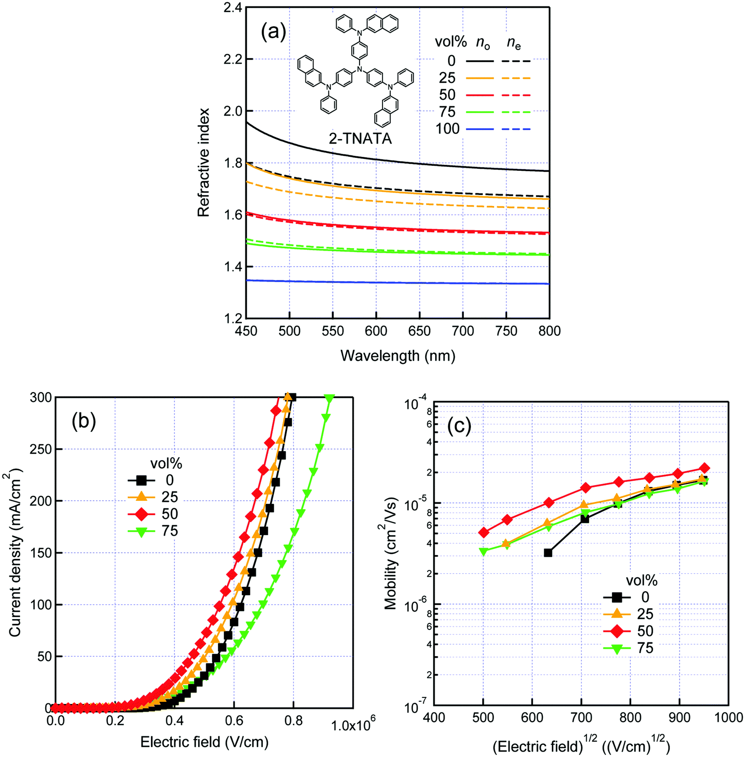 | ||
| Fig. 2 (a) Ordinary and extraordinary refractive indices of neat and co-deposited 2-TNATA:PBVE films with 0, 25, 50, 75, and 100 vol% PBVE. Inset shows the chemical structure of 2-TNATA. (b) J–E characteristics and (c) hole mobilities measured using hole-only devices of ITO/2-TNATA:PBVE (100 nm)/Al (100 nm) with 0, 25, 50, and 75 vol% PBVE. | ||
Fig. 2(b) shows the current density–electric field (J–E) characteristics of hole-only devices of indium tin oxide (ITO)/2-TNATA:PBVE (100 nm)/Al (100 nm) with 0, 25, 50, and 75 vol% PBVE. Interestingly, the J–E characteristics of the devices with the 25 and 50 vol%-PBVE co-deposited 2-TNATA:PBVE films did not deteriorate compared to those of the device with the neat 2-TNATA film (0 vol% PBVE) and showed rather higher current density despite the high content of the insulating PBVE in the films. (Note that when we used the larger-molecular-weight PBVE-L, the 50 vol%-PBVE-L co-deposited 2-TNATA:PBVE-L film showed the deterioration of the J–E characteristics as shown in Fig. S4 (ESI†), which is considered to be due to the chemical decomposition.) When the PBVE content was 75 vol%, the current density became lower than that of the device with the neat 2-TNATA film. Fig. 2(c) shows the hole mobilities in the neat and co-deposited films measured using impedance spectroscopy, where the transit time of holes in the above hole-only devices was determined from the frequency at the maximum negative values of the imaginary part of the impedance28 (see Fig. S5, ESI†). For the neat 2-TNATA film and the 25, 50, and 75 vol%-PBVE co-deposited 2-TNATA:PBVE films, the hole mobilities were on the order of ∼10−5 cm2 V−1 s−1, which is consistent with the value reported for neat 2-TNATA film determined from time-of-flight measurements.29 These interesting results of the electrical properties are in contrast to previously reported results for mixed insulating polycarbonate and OLED materials,30,31 for which the charge mobility significantly decreased with increasing insulator volume content because the distance between hopping sites was enlarged by the insulator.
The results in Fig. 2(a)–(c) show an important fact; the refractive index of HTLs can be effectively lowered via the co-deposition of the fluorinated material without deteriorating the electrical properties for the enhancement of the outcoupling efficiency of OLEDs.19 Similar results were also obtained using another hole transport material, namely 4,4′-bis[N-(1-naphthyl)-N-phenylamino]biphenyl (α-NPD) (Fig. S6, ESI†), indicating the generality of our technique for lowering the refractive index of an HTL in OLEDs. Furthermore, the stable evaporation process of the highly amorphous PBVE without decomposition enables the fabrication of OLEDs with smooth interfaces to control light propagation according to the optical design.
2.3. Phase separation
To clarify why the co-deposition of the insulating PBVE does not deteriorate the electrical properties of the 2-TNATA:PBVE films with 25 and 50 vol% PBVE, we assumed that the 2-TNATA and PBVE phases may have separated in the co-deposited films due to their immiscibility with the large difference in their surface energies, which was confirmed by the large difference in the contact angles of a water droplet on the vacuum-deposited neat 2-TNATA and neat PBVE films (84° vs. 114°). To investigate the periodic structures caused by the phase separation, we performed small-angle X-ray scattering (SAXS) measurements. Fig. 3 shows the SAXS profiles for the co-deposited 2-TNATA:PBVE films with 0, 25, 50, 75, and 100 vol% PBVE on a cyclo-olefin polymer (COP) substrate. The profiles of the neat 2-TNATA and neat PBVE films did not show peaks, whereas those of the 25, 50, and 75 vol%-PBVE films showed a strong peak, which indicates the existence of a periodic structure of different electron density in the co-deposited films. At the peak position of the profiles, the q values are 0.43, 0.56, and 0.67 nm−1 for the 25, 50, and 75 vol%-PBVE films, respectively, which correspond to structural periods of 2π/q = 14, 11, and 9.4 nm, respectively. This result demonstrates that the 2-TNATA and PBVE phases separated in the co-deposited films with a structural period on the order of 10 nm. Furthermore, to clarify the structure of the phase separation, we performed scanning electron microscopy (SEM) observation of the fracture cross sections for the co-deposited films. In the SEM images in Fig. 4, pillar-like structures vertical to the substrate surface caused by phase separation are clearly observed, especially for the 50 vol%-PBVE film, where bright- and dark-contrast parts correspond to the 2-TNATA- and PBVE-rich domains, respectively. In addition, the periods of the nano-sized pillar-like structures in the SEM images are consistent with those estimated from the SAXS profiles, though the surface energies of the Si and COP substrates for SEM and SAXS, respectively, are different as confirmed by the contact angles of a water droplet (5° vs. 98°). Thus, we assume that the nano-sized pillar-like structure is not significantly affected by the underlying layer and is formed also on the ITO surface, whose surface energy (the contact angle of 7°) is close to that of the Si substrate. These well-organized periodic structures show that the co-deposition of 2-TNATA and PBVE causes phase separation via spinodal decomposition on the surface of the films during co-deposition. With increasing PBVE content, the structural period becomes small, because the surface mobility of PBVE molecules during the phase separation is lower than that of 2-TNATA molecules due to the larger molecular weight of ∼6500. Thus, we conclude that the nano-sized phase separation of 2-TNATA and PBVE occurs in the co-deposited films and that it causes the formation of the well-organized pillar-like structures vertical to the substrate surface inside the films.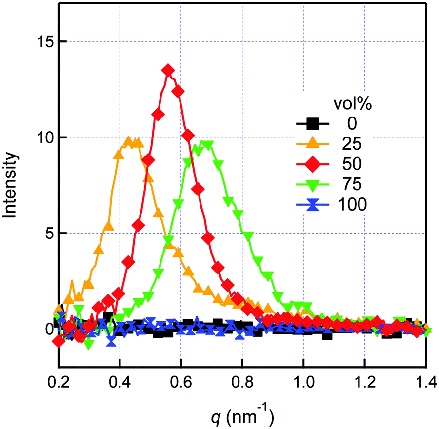 | ||
| Fig. 3 SAXS profiles of 100 nm-thick neat and co-deposited 2-TNATA:PBVE films with 0, 25, 50, 75, and 100 vol% PBVE on a COP substrate. | ||
 | ||
| Fig. 4 Cross-sectional SEM images of 100 nm-thick co-deposited 2-TNATA:PBVE films with (a) 25, (b) 50, and (c) 75 vol% PBVE on a Si(100) substrate. | ||
The formation of the well-organized pillar-like structures contributes to the retention of the paths of hole transport in the co-deposited films. Even for co-deposited films with high insulating PBVE content, the paths of hole transport, which consisted of 2-TNATA-rich domains, were retained and holes could be well transported in the thickness direction. Due to the retention of the pillar-like paths, the hole mobility did not decrease in the co-deposited films, as shown in Fig. 2(c), even though the current density in the 75 vol%-PBVE film decreased, as shown in Fig. 2(b), due to the decrease in the cross-section area for transport. This result is in contrast to previously reported results for mixtures that included a polycarbonate insulator,30,31 where OLED materials were homogeneously dispersed in the polycarbonate via solution processes, which resulted in a significant decrease in charge mobility. Furthermore, it should be noted that the use of a stably evaporable perfluorinated polymer such as the PBVE is important for the formation of well-organized pillar-like structures. For comparison, we also fabricated co-deposited films of 2-TNATA and the small-molecule perfluorinated material C24F50 with 50 vol% C24F50 and investigated the phase-separation structure and electrical properties. As shown in Fig. S7 (ESI†), the SAXS profile of the co-deposited 2-TNATA:C24F50 film did not show a peak representing the formation of a periodic structure, and the J–E characteristics of the co-deposited film deteriorated with decreasing hole mobility by an order compared to that of the neat 2-TNATA film. Thus, the use of the evaporable perfluororesin is important to effectively lower the refractive index of co-deposited films while retaining the paths of hole transport and the electrical properties of the film.
2.4. Interfacial effect
As discussed above, the formation of the paths of hole transport by the phase separation is one of the major factors that explain why the co-deposition of the insulating PBVE does not deteriorate the electrical properties of the co-deposited films. However, it does not explain why the J–E characteristics of the hole-only devices with the 25 and 50 vol%-PBVE films are superior to those of the devices with the neat 2-TNATA film.To understand its mechanism, we investigated whether the electrical properties of these devices are improved in the bulk of the films or at the interfaces of the electrodes. First, we supposed that many free holes may have been generated in the bulk of the co-deposited film due to the charge transfer from 2-TNATA to PBVE, because PVBE can stably hold electrons as an electret material.23–25 However, in the visible/near-infrared (NIR) absorption spectrum of the co-deposited film, shown in Fig. S8 (ESI†), no absorption band corresponding to a charge-transfer state was observed, indicating that free holes are not generated in the bulk by the co-deposition of the PBVE. Then, for further investigation, we fabricated various hole-only devices shown in Fig. 5(a), where all co-deposited layers were 2-TNATA:PBVE layers with 50 vol% PBVE. Devices A and B are the same as the devices whose J–E characteristics are shown in Fig. 2(b) (0 and 50 vol% devices, respectively), and Devices C–F have a locally co-deposited region. The J–E characteristics of these devices are shown in Fig. 5(b). Interestingly, only the devices that had a co-deposited layer at the interface of the ITO anode (Devices B, C, and D) showed improved characteristics compared to those of Device A, which had a single neat 2-TNATA film. On the other hand, the J–E characteristics of Devices E and F significantly deteriorated compared to those of Device A even though they contained a co-deposited layer inside the devices. This severe deterioration for Devices E and F would include the effect of the inhomogeneous distribution of the electric field, which is smaller in the neat 2-TNATA layer with a relatively high dielectric permittivity than in the co-deposited layer with a relatively low one. Nevertheless, the distinct difference in the J–E characteristics of Devices E and F compared to those of Devices B, C, and D clearly shows that the electrical properties of the devices with a co-deposited layer are improved not in the bulk of the layer but at the ITO interface. The improvement at the ITO interface is also confirmed by the J–E characteristics of the hole-only devices of ITO/2-TNATA:PBVE/Al in a double logarithmic plot (Fig. S9, ESI†). With increasing volume content of the PBVE, the injection current at low electric fields monotonically increases, showing that the existence of the PBVE at the ITO interface improves hole injection and the J–E characteristics of the co-deposited films.
 | ||
| Fig. 5 (a) Device structures and (b) J–E characteristics of Devices A–F fabricated to investigate the effect of locally co-deposited region. The interfaces between the ITO anode and co-deposited films, which improve hole injection, are indicated by red lines in (a). (c) J–E characteristics of devices of ITO/PBVE (x nm)/2-TNATA [(100 − x) nm]/Al (100 nm) in the range of x = 0–7. For comparison, the J–E characteristics of the device with a thin co-deposited 2-TNATA:PBVE layer (Device C) are also shown. | ||
A plausible mechanism of the improvement at the ITO interface is a tunneling effect enhanced via an insulating layer of the PBVE, which has high resistivity. It is known that inserting a thin insulating layer with high resistivity at the interface of an electrode enhances charge injection via tunneling.32,33 In particular, the effect of the insertion of a thin layer of an insulating perfluoro material was investigated in a previous study.34 An improvement in hole injection caused by the tunneling effect was observed when the thin insulating layer with an appropriate small thickness was inserted. To investigate whether such improvement occurs with the PBVE, we fabricated devices with a thin PBVE layer of ITO/PBVE (x nm)/2-TNATA [(100 − x) nm]/Al (100 nm) in the range of x = 0–7 and measured their J–E characteristics. As shown in Fig. 5(c), hole injection was improved by the insertion of the thin PBVE layer with a thickness of 1–4 nm, indicating a tunneling effect via the thin PBVE layer. From the similarity of the improvements of the J–E characteristics observed in these devices with the thin PBVE layer and the device with the thin co-deposited 2-TNATA:PBVE layer (Device C), we conclude that thin pieces of the PBVE exist in some parts of the interface between the ITO electrode and 2-TNATA-rich domains in the devices with the co-deposited 2-TNATA:PBVE films and that they improve hole injection at the ITO interface.
It should be noted, however, that not all the observed electrical properties are fully explained only by the phase separation and the tunneling effect. For example, co-depositing the PBVE with electron transport materials severely deteriorates the electrical properties of films (Fig. S10, ESI†). This shows the asymmetric effect of the PBVE on positive and negative charges and also suggests the possibility that the electret characteristic of PBVE (i.e., it stably holds electrons) affects the electrical properties of the co-deposited films. Thus, although we determined that one of the major factors that improve hole injection in the devices with a co-deposited film is the tunneling effect, there would also be other factors affecting injection and transport, which are currently under investigation.
2.5. Outcoupling enhancement of OLEDs
To demonstrate the effect of the co-deposited layer with the low refractive index on the outcoupling efficiency of OLEDs, we fabricated two phosphorescent OLEDs and compared their performances while discussing the results of optical simulations; one is the reference device, which has a normal HTL, and the other is “the low-index device”, which has the low-index HTL of a co-deposited 2-TNATA:PBVE film with 50 vol% PBVE. The structure of the former is glass/ITO (75 nm)/2-TNATA:HAT-CN (1 wt%, 20 nm)/2-TNATA (40 nm)/α-NPD (10 nm)/CBP:Ir(ppy)2(acac) (8 wt%, 15 nm)/TPBi (65 nm)/LiF (1 nm)/Al (100 nm), and that of the latter is glass/ITO (75 nm)/2-TNATA:PBVE (50 vol%, 70 nm)/α-NPD (10 nm)/CBP: Ir(ppy)2(acac) (8 wt%, 15 nm)/TPBi (60 nm)/LiF (1 nm)/Al (100 nm). The chemical structures and the energy diagrams of the materials used in the OLEDs are shown in Fig. 6(a) and (b), respectively, where the energy levels of PBVE were taken from the literature.24 For the reference device, we locally doped a small amount of HAT-CN into the HTL of 2-TNATA at the ITO interface to compensate for the slight difference between the electrical properties of the neat 2-TNATA and co-deposited 2-TNATA:PBVE films. Using SETFOS 4.6 software (FLUXiM AG) with the optical constants of each layer determined from ellipsometry (Fig. S11, ESI†), the thicknesses of the HTL of 2-TNATA or 2-TNATA:PBVE and the electron transport layer (ETL) of TPBi in these OLEDs were optimized based on optical simulations of the optical mode fractions so that the outcoupling efficiencies were maximized (Fig. S12, ESI†). Fig. 6(c) shows the dependence of the optical mode fractions on the HTL thickness estimated from the optical simulations. Comparing the fractions at the maxima of the outcoupling efficiency, at 60 nm for the reference device and 70 nm for the low-index device, the outcoupling efficiency of the low-index device (33.0%) is significantly enhanced compared to that of the reference device (26.8%) by a factor of 1.23, demonstrating a distinct effect of the low-index co-deposited layer with the PBVE on the outcoupling efficiency, as expected. The thicker optimal thickness of the HTL of the low-index device reflects its lower refractive index, with which the optical thickness of the HTL of the low-index device is similar to that of the reference device. With the low-index layer, the fractions of the waveguide and plasmon modes are effectively suppressed, and their decreases contribute to the significant enhancement of the fraction of the outcoupling mode. We note that the effect of the decrease in the birefringence of the HTL (see Fig. 2(a)) would be also slightly included in this outcoupling enhancement.10 Furthermore, we emphasize that the fraction of the substrate mode does not change, which indicates the compatibility of our technique with conventional techniques such that based on a microlens array. This makes it possible to further additively increase outcoupling efficiency by using both of the low-index layer and external optical elements. | ||
| Fig. 6 (a) Chemical structures and (b) energy diagrams of the materials used in the prepared OLEDs. (c) Dependence of the optical mode fractions of the reference and low-index devices on the HTL thickness estimated from optical simulations. (d) J–V–L characteristics and (e) EQEs of the reference and low-index devices. Inset in (e) shows the electroluminescence spectra of the two devices at a current density of 1 mA cm−2. | ||
The experimental results in Fig. 6(d) show that the current density–voltage (J–V) characteristics and the turn-on voltages of front luminance (L) of the two devices were quite similar even though the low-index layer with the PBVE was used in the low-index device. The electroluminescence spectra of the two devices, shown in the inset of Fig. 6(e), were also the same. However, the EQEs of the two devices, which were determined from the front luminance and the angular distribution of electroluminescence (Fig. S13, ESI†), showed a distinct difference, as shown in Fig. 6(e); the EQE of the low-index device was significantly higher than that of the reference device in the whole range of the current density. The maxima of the EQEs at a low current density were 23.5% and 28.6% for the reference and low-index devices, respectively, demonstrating an enhancement of the EQE by a factor of 1.22, which is almost the same as the simulated factor of the outcoupling enhancement (1.23). Although the enhancement factor depends on the current density, it is considered to be due to the slight difference in the carrier balance of the two devices under high voltages. Furthermore, considering the photoluminescent (PL) quantum yield of 8 wt%-doped Ir(ppy)2(acac) in CBP of 0.836, which was experimentally determined, the upper limits of the EQEs of the two devices were simulated to be 22.4% and 27.6%, respectively, which correspond well to the above experimental maximum values of the EQEs. These results show that the outcoupling enhancement was surely caused in the low-index device, as expected from the optical simulations, and demonstrate that the outcoupling efficiency can be significantly enhanced by the low-index layer actively controlled with the PBVE.
In addition, to confirm the generality of the effect of a low-index layer, we also fabricated an OLED in which the PBVE was co-deposited with another hole transport material, namely α-NPD, and compared its characteristics to those of a reference OLED without a low-index layer (Fig. S14, ESI†). Similar to the OLED with the co-deposited 2-TNATA:PBVE layer, the OLED with an α-NPD:PBVE layer showed an enhancement of EQEs by a factor of 1.20, demonstrating that our technique of co-depositing the PBVE in an HTL is valid for different hole transport materials. Although the experimental demonstrations with OLEDs in this study are limited to the two examples, we believe that our technique can be applied to many different fluorescent, phosphorescent, and TADF OLEDs to actively control the refractive index of HTLs and significantly enhance their outcoupling efficiencies and EQEs.
3. Conclusions
To actively control the refractive index of the charge transport layers in OLEDs in a wide range to significantly enhance outcoupling efficiency, we synthesized a perfluorinated fluororesin of PBVE, which has a low refractive index, high amorphousness, and a small Mw of 10700, and applied it to the HTLs of OLEDs by co-deposition. The PBVE can be stably evaporated by a vacuum deposition process without chemical decomposition, as done for conventional OLED materials. The portion with a relatively small molecular weight is preferentially evaporated, resulting in a small Mw of 6500 and a low polydispersity of 1.1 of the evaporant. The co-deposition of the PBVE with the hole transport material 2-TNATA effectively lowers the refractive index of the film; the refractive index of the co-deposited 2-TNATA:PBVE film with 50 vol% PBVE is 1.56 at 550 nm, which is much lower than that achieved by solely selecting a low-index OLED material. Interestingly, the electrical properties of the hole-only devices with the co-deposited 2-TNATA:PBVE films with 25 and 50 vol% PBVE did not deteriorate compared to that of the device with the neat 2-TNATA film but instead showed improved hole injection even though the films contained a large volume content of the insulating PBVE. The retention of the electrical properties of the co-deposited films can be partly explained by the phase separation of 2-TNATA and PBVE, which causes the formation of well-organized nano-sized pillar-like structures in the co-deposited films and contributes to the retention of the paths of hole transport consisting of 2-TNATA-rich domains in the thickness direction. In addition, the existence of the PBVE at the interface of the ITO anode improves hole injection by the tunneling effect via a thin insulating PBVE layer. A phosphorescent OLED with the low-index co-deposited 2-TNATA:PBVE layer as the HTL clearly demonstrated a significant enhancement of the outcoupling efficiency by a factor of 1.22, which is consistent with the estimation from optical simulations. The simulations also show that the fraction of the substrate mode does not change, which means that a further additive increase of outcoupling efficiency is possible by using both the low-index layer and external optical elements such as a microlens array.
The use of the PBVE for active refractive index control and outcoupling enhancement can be applied only by co-depositing it with a hole transport material and does not require any additional experimental process or equipment other than those of the normal OLED fabrication process. Furthermore, the material cost of the PBVE is not more than that of conventional OLED materials. Thus, our method can be applied to many types of OLED as a general technique to significantly enhance their outcoupling efficiency without increasing production cost. We believe that the active refractive index control demonstrated in this study will be a major strategy for achieving further high-efficiency OLEDs.
4. Experimental section
General
The sublimed OLED materials used in this study were purchased from Luminescence Technology Co., except for CBP and HAT-CN, which were purchased from e-Ray Optoelectronics Technology. All the vacuum depositions of the organic films were performed at a rate of ∼2 Å s−1 under a vacuum of <1 × 10⁻⁴ Pa. The AFM images of the surface of 10 nm-thick films on a Si(100) substrate were obtained using an Agilent Technologies 5500 scanning probe microscope in tapping mode. The out-of-plane and in-plane XRD patterns of 100 nm-thick films on a Si(100) substrate were measured with a SmartLab X-ray diffractometer (Rigaku Co.) under Cu Kα (λ = 1.54178 Å) radiation at 45 kV and 200 mA. The contact angles of a water droplet on the films were measured using an LSE-ME2 contact angle meter (NiCK Co.). The visible/NIR absorption spectra of 50 nm-thick films on a fused silica substrate were measured using a V-670 UV-visible/NIR spectrophotometer (JASCO Co.).Synthesis of PBVE
30 g of perfluoro butenyl vinyl ether, 30 g of 1,1,1,2,2,3,3,4,4,5,5,6,6-tridecafluorohexane (TFH), 0.35 g of methanol, and 0.45 g of diisopropyl peroxydicarbonate, as a polymerization initiator, were put into a glass reactor with an internal capacity of 50 mL. The interior of the system was replaced with nitrogen gas, and then polymerization was carried out at 40 °C for 24 h. The obtained solution was poured into a polytetrafluoroethylene boat and heated at 100 °C on a hot plate for 5 h, and then vacuum-dried at 100 °C for 12 h to obtain polymer A. Polymer A was heating at 330 °C under an air atmosphere to obtain polymer B. The characteristic absorption at 1883 cm−1 derived from –COF groups was confirmed in the IR absorption spectrum of the compression-formed film of polymer B. Then, a 1 L autoclave made of nickel was evacuated to −760 torr, and 900 g of 3 wt% polymer B solution in perfluorotributylamine was charged into the autoclave under reduced pressure. Fluorine gas diluted by nitrogen gas to a concentration of 5 vol% was introduced into the system to 0.8 MPa G, followed by treatment under stirring for 20 h at a temperature of 195 °C, to obtain polymer C. The lack of the characteristic absorption at 1883 cm−1 derived from –COF groups was confirmed in the IR absorption spectrum of the compression-formed film of polymer C. Polymer C is used as the PBVE. The refractive index of the PBVE film measured using ellipsometry was 1.34 at 550 nm. The saturated vapor pressure of the PBVE measured using vacuum differential thermal analysis was 2.6 × 10⁻³ Pa at 300 °C.SEC
The molecular weight distributions of the PBVE were determined by SEC using a Nexera X2 liquid chromatography system (Shimadzu Co.) with 1,1,1,2,3,4,4,5,5,5-decafluoro-3-methoxy-2-(trifluoromethyl)pentane/hexafluoroisopropyl alcohol (85/15 volume ratio) as a mobile phase solvent and PLgel MIXED-C (Agilent Technologies) as a column. Using the solutions of standard samples of polymethyl methacrylate with known molecular weights of the peak maxima (EasiVial, Agilent Technologies), a calibration curve was prepared from the relationship between the known molecular weight and the detected retention time at the peak top (Fig. S1, ESI†). Then, the solutions of the PBVE before and after evaporation with TFH were injected, and their molecular weight distributions were determined using the calibration curve. During the preparation of the evaporant solution, a substrate with a vacuum-deposited PBVE film was immersed into TFH to dissolve the evaporant, and then the solution was dried once and dissolved again with 200 μL of TFH. During the preparation of the solution of the residue after evaporation, droplets of TFH were added into the evaporation boat to dissolve the residue, and then the solution was dried once and dissolved again with 200 μL of TFH.Ellipsometry
To measure the optical constants (refractive indices and extinction coefficients) of the organic films and their anisotropies, variable angle spectroscopic ellipsometry (VASE) measurements were performed using an M-2000U fast spectroscopic ellipsometer (J.A. Woollam Co.). Single-layer samples of the organic films with a thickness of ∼100 nm on a Si(100) substrate were used. Ellipsometric parameters Ψ and Δ were measured for each sample in steps of 1.6 nm throughout the spectral region from 245 to 1000 nm at seven incident angles from 45° to 75° in steps of 5°. The analysis of the combined VASE data for each sample was performed using WVASE32 software (J.A. Woollam Co.), where the dielectric functions of the organic films were modeled by general oscillators composed of Gaussian bands with uniaxial anisotropy. The optical constants of the ITO film on a glass substrate were also measured using similar VASE measurements and analysis, where the dielectric functions were modeled by general oscillators composed of Tauc-Lorentz and Drude bands assuming isotropy.Optical simulations
The optical simulations of the optical mode fractions and the angular electroluminescence distributions of the OLEDs were performed using SETFOS 4.6 software (FLUXiM AG), where the optical constants determined from the VASE measurements were used, and the optical anisotropy of organic layers was taken into consideration. For the simulations, the PL spectrum and quantum yield of the emitting layer were experimentally measured using a Quantaurus-QY absolute PL quantum yield spectrometer (Hamamatsu Photonics K.K.). The orientation factor of the transition dipole moments of Ir(ppy)2(acac) in the host of CBP films was assumed to be 0.267,35 and the emission site was assumed to be at the center of the emitting layer.Device fabrication and measurements
All the devices for the electrical measurements were fabricated with a device area of 2 × 2 mm2 on an ITO glass substrate, which was cleaned in advance with a detergent, acetone, and 2-propanol and then dry-cleaned for 15 min by exposure to UV-ozone. The J–V characteristics of the devices were measured using a Keithley 2401 source meter. The impedance spectroscopy measurements were performed using an IM3570 impedance analyzer (Hioki E.E. Co.), where a DP-3003S DC power supply (Custom Co.) was connected through a circuit to apply a DC bias to the devices. The impedance of the devices was measured with a 200 mV AC voltage with frequencies of 10 Hz–1 MHz while the DC bias voltage was varied. The front luminance and spectra of the electroluminescence of the OLEDs were measured using a CS-200 chroma meter (Konica Minolta Japan Inc.) and a C10083CA mini-spectrometer (Hamamatsu Photonics K.K.), respectively. The angular distributions of the electroluminescence of the OLEDs were measure under a current density of 1 mA cm−2 using the mini-spectrometer and an SGSP-60YAW-0B motorized rotation stage (Sigmakoki Co., Ltd).SAXS
SAXS profiles of 100 nm-thick films deposited on a COP substrate were measured using a NANO-Viewer highly-brilliant small-angle X-ray scattering system (Rigaku Co.) equipped with a charge-coupled device detector under Cu Kα radiation at an applied voltage and filament current of 40 kV and 30 mA, respectively. The distance between the sample film and detector was ∼650 mm, and the exposure time was 20 min for each sample.SEM
To prepare the samples for SEM observation of the fracture cross section of the co-deposited films, 100 nm-thick films were fabricated on a Si(100) substrate, which was then cleanly broken. A 1 nm-thick Pt layer was then ion-sputtered onto the fracture cross section of the films to avoid surface charge-up. SEM observation were performed using an SU8230 ultrahigh-resolution scanning electron microscope (Hitachi High-Technologies Co.) with an accelerating voltage of 2 kV and an emission current of 10 μA.Author contributions
D. Y. conceived the research concept and supervised the whole research, assisted by Y. K. and Y. N. D. Y. and T. A. proposed the use of the PBVE. T. A. synthesized the PBVE. T. K. performed the SEC analysis with support by T. A. and K. T. D. Y., T. S., and Y. S. performed the ellipsometry analysis. T. S., Y. S., M. A., and W. A. performed the electrical measurements of the hole- and electron-only devices with support by Y. N. T. S. and Y. O. performed the mobility measurements. T. S. and T. M. performed the SAXS measurements. CM performed the SEM observation with support by T. A., K. T., and T. M. D. Y., T. S., T. A., K. T., T. M., Y. K., and Y. N. discussed the mechanisms of the electrical conduction and phase separation. D. Y. and Y. S. performed the optical simulations and designed the OLEDs. T. S. and Y. S. performed the OLED experiments. D. Y. wrote the manuscript with support by T. A., T. M., Y. K., and Y. N.Conflicts of interest
The authors declare no conflicts of interest.Acknowledgements
The authors acknowledge Prof. Hisao Ishii (Chiba University) for fruitful discussion on the electrical properties of the co-deposited films. The authors also acknowledge Prof. Akito Masuhara and Dr Masaki Takeda (Yamagata University) for their support in the measurements of the visible/NIR absorption spectra. This work was financially supported in part by AGC Research Collaboration System and KAKENHI grants (grant numbers 25708038 and 15K13768) from the Japan Society for the Promotion of Science (JSPS).References
- Y. Kawamura, K. Goushi, J. Brooks, J. J. Brown, H. Sasabe and C. Adachi, Appl. Phys. Lett., 2005, 86, 071104 CrossRef.
- H. Kaji, H. Suzuki, T. Fukushima, K. Shizu, K. Suzuki, S. Kubo, T. Komino, H. Oiwa, F. Suzuki, A. Wakamiya, Y. Murata and C. Adachi, Nat. Commun., 2015, 6, 8476 CrossRef CAS.
- K. Saxena, V. K. Jain and D. S. Mehta, Opt. Mater., 2009, 32, 221 CrossRef CAS.
- M. C. Gather and S. Reineke, J. Photon. Energy, 2015, 5, 057607 CrossRef.
- A. Salehi, X. Fu, D.-H. Shin and F. So, Adv. Funct. Mater., 2019, 29, 1808803 CrossRef.
- D. Yokoyama, J. Mater. Chem., 2011, 21, 19187 RSC.
- J. Frischeisen, D. Yokoyama, A. Endo, C. Adachi and W. Brütting, Org. Electron., 2011, 12, 809 CrossRef CAS.
- K.-H. Kim and J.-J. Kim, Adv. Mater., 2018, 30, 1705600 CrossRef PubMed.
- C.-K. Moon, S.-Y. Kim, J.-H. Lee and J.-J. Kim, Opt. Express, 2015, 23, A279 CrossRef CAS.
- M. K. Callens, D. Yokoyama and K. Neyts, Opt. Express, 2015, 23, 21128 CrossRef CAS PubMed.
- M. Schmid, T. Morgenstern and W. Brütting, Org. Electron., 2018, 62, 216 CrossRef CAS.
- D. Yokoyama, K. Nakayama, T. Otani and J. Kido, Adv. Mater., 2012, 24, 6368 CrossRef CAS PubMed.
- L. H. Smith and W. L. Barnes, Org. Electron., 2006, 7, 490 CrossRef CAS.
- K. Fehse, K. Walzer, K. Leo, W. Lövenich and A. Elschner, Adv. Mater., 2007, 19, 441 CrossRef CAS.
- C. Fuchs, P.-A. Will, M. Wieczorek, M. C. Gather, S. Hofmann, S. Reineke, K. Leo and R. Scholz, Phys. Rev. B: Condens. Matter Mater. Phys., 2015, 92, 245306 CrossRef.
- C.-Y. Lu, M. Jiao, W.-K. Lee, C.-Y. Chen, W.-L. Tsai, C.-Y. Lin and C.-C. Wu, Adv. Funct. Mater., 2016, 26, 3250 CrossRef CAS.
- H. Shin, J.-H. Lee, C.-K. Moon, J.-S. Huh, B. Sim and J.-J. Kim, Adv. Mater., 2016, 28, 4920 CrossRef CAS PubMed.
- A. Salehi, S. Ho, Y. Chen, C. Peng, H. Yersin and F. So, Adv. Opt. Mater., 2017, 5, 1700197 CrossRef.
- D. Yokoyama, Y. Suzuki and W. Aita, IMID2015, 49-1, Daegu, Korea, Aug. 2015.
- T. Watabe, R. Yamaoka, N. Ohsawa, A. Tomida, S. Seo and S. Yamazaki, SID2018 Digest, 2018, pp. 332.
- J. S. Price, B. Wang, T. Kim, A. J. Grede, J. M. Sandoval, R. Xie, Y. Shen, D. R. Adams, M. J. Eller, A. Sokolov, S. Mukhopadhyay, P. Trefonas, E. D. Gomez, E. A. Schweikert and N. C. Giebink, Appl. Phys. Lett., 2018, 113, 263302 CrossRef.
- T. C. Nason, J. A. Moore and T.-M. Lu, Appl. Phys. Lett., 1992, 60, 1866 CrossRef CAS.
- Y. Sakane, Y. Suzuki and N. Kasagi, J. Micromech. Microeng., 2008, 18, 104011 CrossRef.
- T. T. Dao, T. Matsushima, R. Friedlein and H. Murata, Org. Electron., 2013, 14, 2007 CrossRef CAS.
- T. T. Dao, T. Matsushima and H. Murata, Org. Electron., 2012, 13, 2709 CrossRef CAS.
- M. Shibata, Y. Sakai and D. Yokoyama, J. Mater. Chem. C, 2015, 3, 11178 RSC.
- J.-G. Liu and M. Ueda, J. Mater. Chem., 2009, 19, 8907 RSC.
- D. C. Tripathi, A. K. Tripathi and Y. N. Mohapatra, Appl. Phys. Lett., 2011, 98, 033304 CrossRef.
- S. C. Tse, K. C. Kwok and S. K. So, Appl. Phys. Lett., 2006, 89, 262102 CrossRef.
- M. Stolka, J. F. Yanus and D. M. Pai, J. Phys. Chem., 1984, 88, 4707 CrossRef CAS.
- H. Tokuhisa, M. Era, T. Tsutsui and S. Saito, Appl. Phys. Lett., 1995, 66, 3433 CrossRef CAS.
- S. T. Zhang, X. M. Ding, J. M. Zhao, H. Z. Shi, J. He, Z. H. Xiong, H. J. Ding, E. G. Obbard, Y. Q. Zhan, W. Huang and X. Y. Hou, Appl. Phys. Lett., 2004, 84, 425 CrossRef CAS.
- J. M. Zhao, S. T. Zhang, X. J. Wang, Y. Q. Zhan, X. Z. Wang, G. Y. Zhong, Z. J. Wang, X. M. Ding, W. Huang and X. Y. Hou, Appl. Phys. Lett., 2004, 84, 2913 CrossRef CAS.
- Z. Wu, L. Wang, H. Wang, Y. Gao and Y. Qiu, Phys. Rev. B: Condens. Matter Mater. Phys., 2006, 74, 165307 CrossRef.
- C. Mayr and W. Brütting, Chem. Mater., 2015, 27, 2759 CrossRef CAS.
Footnote |
| † Electronic supplementary information (ESI) available. See DOI: 10.1039/d1tc02478g |
| This journal is © The Royal Society of Chemistry 2021 |