
 Open Access Article
 This Open Access Article is licensed under a
 Creative Commons Attribution 3.0 Unported Licence
In0.5Ga0.5N layers by atomic layer deposition†
Polla
Rouf
 *,
Justinas
Palisaitis
,
Babak
Bakhit
,
Nathan J.
O'Brien
and
Henrik
Pedersen
*,
Justinas
Palisaitis
,
Babak
Bakhit
,
Nathan J.
O'Brien
and
Henrik
Pedersen
Department of Physics, Chemistry and Biology, Linköping University, Linköping SE-58183, Sweden. E-mail: polla.rouf@liu.se
First published on 14th September 2021
Abstract
We present an ALD approach to metastable In1−xGaxN with 0.1 < x < 0.5 based on solid In- and Ga-precursors that were co-sublimed into the deposition chamber in one pulse. A near In0.5Ga0.5N film with a bandgap value of 1.94 eV was achieved on a Si(100) substrate. Epitaxial In1−xGaxN(0002) was successfully grown directly on the 4H–SiC(0001) substrate.
Alloying group 13-nitrides to ternary phases allows tuning of the bandgap from 6.2 eV for pure AlN1 down to 0.7 eV for pure InN.2 The bandgap of In1−xGaxN can theoretically span from UV to IR (3.4–0.7 eV), including the whole visible light range by varying x, making it promising material for optoelectronic applications.3,4 However, the ability to vary the composition of In1−xGaxN is limited by the theoretically predicted metastability of In1−xGaxN for 0.05 < x < 0.95, which leads to phase separation into their binary materials.5 The deposition of In1−xGaxN is also hindered by the low thermal stability of InN, which decomposes into In metal and N2 at around 500 °C.6 Experimental results lined up with the predicted metastability, albeit x = 0.8 (20 at% In) has been shown in thin films deposited by chemical vapor deposition (CVD).4,7–10 CVD is not ideal for In1−xGaxN due to the high temperatures (>500 °C) required to reach sufficient decomposition of NH311 and typically results in low In content, phase separation, and In droplets.8,10 A low temperature deposition technique is strongly preferred for In1−xGaxN with x close to 0.5. Atomic layer deposition (ALD) is a low temperature alternative to CVD, in which the precursors are pulsed sequentially into the reactor. We have recently shown that ALD is a promising technique to deposit InN thin films with excellent structural quality.12
The sequential pulsing of the precursors in ALD presents a challenge to depositing a homogeneous ternary material as only one precursor can be pulsed into the reactor at a time. Ternary materials are therefore deposited by ALD as stacks of two binary materials. In1−xGaxN could therefore be deposited as layers of InN and GaN in an ABAB⋯CBCB… super-cycle approach where A and C are In- and Ga-precursors, respectively, and B is the N-reactant. By varying the number of cycles for each binary material, the overall composition of the ternary material can be tuned. This approach relies on diffusion of the two binary materials to form a homogeneous ternary phase. Otherwise, a multilayer of InN/GaN is obtained. This ALD approach has been used to obtain In1−xGaxN with x ranging from 0.15–0.85 using trimethylindium and trimethylgallium.13 Herein, we present an alternative method to depositing ternary materials by introducing both metal precursors with a single pulse. This renders mixing of the metals in both the growth direction and in the growth plane. This was achieved by mixing and co-subliming two solid metal precursors into the ALD chamber. Somewhat similar ALD processes have been reported for ternary materials, albeit with two different precursor sources co-injected from two gas lines.14–16
We have previously investigated ALD of InN and GaN using tris(1,3-diisopropyltriazenide)indium(III)12 (1) and gallium(III)17 (2) (Fig. S1, ESI†). Rendering stable ALD behavior with self-limiting deposition, wide temperature ranges where the growth per cycle is not affected by the temperature and a high growth per cycle, combined with good structural and electronic properties of the materials. In both studies, we found a sublimation temperature of 120–130 °C to be optimal for each precursor and epitaxial films were obtained at 350 °C for both InN and GaN on 4H–SiC(0001). In this study, we mixed both precursors in the sublimator and co-sublimed them into the reaction chamber in a single pulse. ALD of In1−xGaxN was then undertaken using the same previously optimized parameters as for the binary nitrides with NH3 plasma as the nitrogen source (see ESI† for experimental details). Initial trials were conducted on Si(001) and it was found that x in In1−xGaxN can be controlled (0.1 < x < 0.5) by the sublimation- and deposition temperatures, and by the mixing ratio of 1 and 2 (see ESI† for details). Growth of epitaxial In1−xGaxN was attempted on 4H–SiC(0001) as it is a suitable substrate for both epitaxial InN and GaN.12,17 When depositing directly on 4H–SiC, without a nucleation layer, using a 1![[thin space (1/6-em)]](https://www.rsc.org/images/entities/char_2009.gif) :1 (In:Ga) precursor mix, sublimation temperature 130 °C and deposition temperature 350 °C, In1−xGaxN was obtained. In the θ–2θ XRD measurement (Fig. 1a), the peak ascribed to In1−xGaxN(0002) is a wide, unsymmetrical triplet, indicating a compositional difference in the film. The peak at 32.0° is closer to InN(31.3°) indicating In-rich In1−xGaxN while the peak at 33.9° is closer to GaN(34.5°) indicating Ga-rich In1−xGaxN. The a-lattice constants for 4H–SiC, GaN and InN are 3.079 Å,18 3.189 Å3 and 3.548 Å,19 respectively, while the lattice constant for In1−xGaxN will vary between the InN and GaN values depending on x. This compositional difference could possibly be explained by stress relaxation in the film. Ga-rich In1−xGaxN was obtained closer to the interface due to the better lattice match with the substrate while further away higher In content can be incorporated without inducing an increasing stress. The compositional difference obtained in the film could also be related to the behavior of the precursors on the surface. We have previously observed that ALD of GaN with 2 has a lower nucleation delay (∼16 ALD cycles) compared to InN with 1 (∼50 ALD cycles). This indicates that GaN with 2 grows easier directly on the surface, which would lead to initial Ga-rich In1−xGaxN. However, 1 has a higher surface reactivity, which is displayed by its higher growth per cycle (1.2 Å per cycle) for InN in comparison to that of 2 for GaN (0.3 Å per cycle). This would allow 1 to dominate after some initial growth and could be the reason for In-rich In1−xGaxN further away from the interface. The compositional difference could be affected by all these factors and each could be dominant at different growth stages.
:1 (In:Ga) precursor mix, sublimation temperature 130 °C and deposition temperature 350 °C, In1−xGaxN was obtained. In the θ–2θ XRD measurement (Fig. 1a), the peak ascribed to In1−xGaxN(0002) is a wide, unsymmetrical triplet, indicating a compositional difference in the film. The peak at 32.0° is closer to InN(31.3°) indicating In-rich In1−xGaxN while the peak at 33.9° is closer to GaN(34.5°) indicating Ga-rich In1−xGaxN. The a-lattice constants for 4H–SiC, GaN and InN are 3.079 Å,18 3.189 Å3 and 3.548 Å,19 respectively, while the lattice constant for In1−xGaxN will vary between the InN and GaN values depending on x. This compositional difference could possibly be explained by stress relaxation in the film. Ga-rich In1−xGaxN was obtained closer to the interface due to the better lattice match with the substrate while further away higher In content can be incorporated without inducing an increasing stress. The compositional difference obtained in the film could also be related to the behavior of the precursors on the surface. We have previously observed that ALD of GaN with 2 has a lower nucleation delay (∼16 ALD cycles) compared to InN with 1 (∼50 ALD cycles). This indicates that GaN with 2 grows easier directly on the surface, which would lead to initial Ga-rich In1−xGaxN. However, 1 has a higher surface reactivity, which is displayed by its higher growth per cycle (1.2 Å per cycle) for InN in comparison to that of 2 for GaN (0.3 Å per cycle). This would allow 1 to dominate after some initial growth and could be the reason for In-rich In1−xGaxN further away from the interface. The compositional difference could be affected by all these factors and each could be dominant at different growth stages.
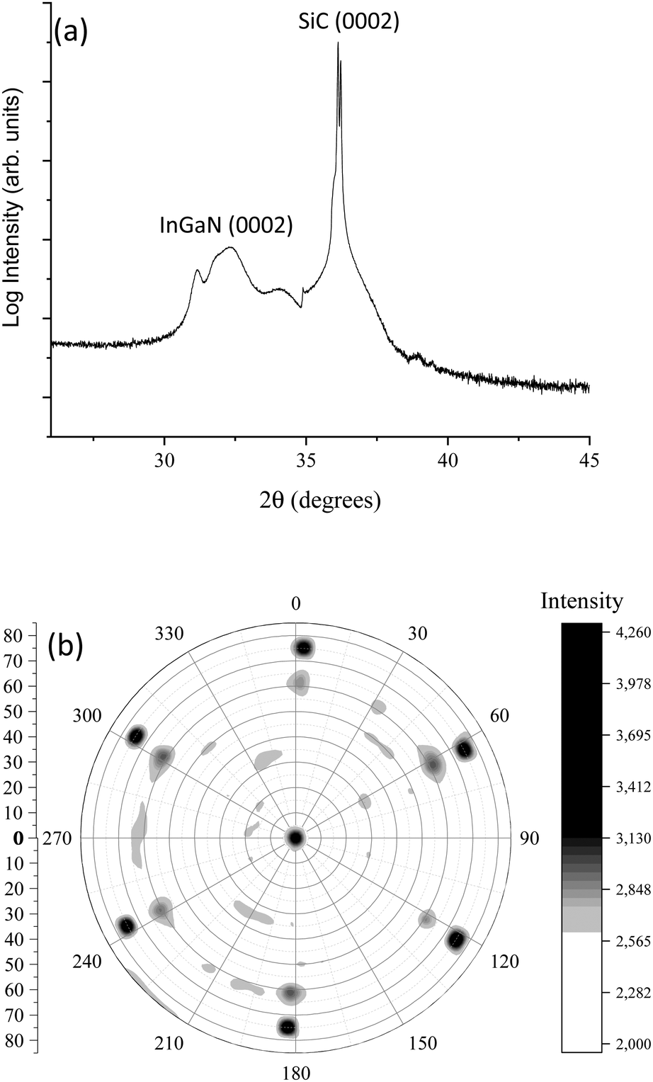 | ||
Fig. 1 (a) The θ–2θ XRD and (b) Pole figure of the (10![[1 with combining macron]](https://www.rsc.org/images/entities/char_0031_0304.gif) 1) plane of ∼ 60 nm In1−xGaxN on 4H–SiC deposited at 350 °C. 1) plane of ∼ 60 nm In1−xGaxN on 4H–SiC deposited at 350 °C. | ||
Pole figure measurement was conducted to determine the in-plane orientation of the In1−xGaxN film. The XRD pole figure for the (101) plane was constructed showing two sets of six poles at different Φ values (Fig. 1b). The outer six poles with a higher Φ value correspond to the 4H–SiC substrate while the inner six poles correspond to the In1−xGaxN film, confirming the epitaxial relation. It should be noted that the substrate poles have a higher intensity than the In1−xGaxN poles. This could be due to the compositional difference in the film, which was also observed in the θ–2θ measurement. The similar, but not identical, Φ values of InN (101) and GaN (101) would broaden the In1−xGaxN pole if the film composition is not uniform. The epitaxial relationship was found to be In1−xGaxN[0002]∣∣4H–SiC[0001] and In1−xGaxN [101]∣∣4H–SiC [101] meaning that the In1−xGaxN hexagonal crystals grow exactly on top of the substrate crystals. There is no misalignment between the substrate and film poles as they line up precisely, indicating no twisting of the InGaN crystals with respect to the substrate.
The structural and crystalline properties of the In1−xGaxN film were further analyzed using scanning transmission electron microscopy (STEM) with high angle annular dark field (HAADF) imaging and selected area electron diffraction (SAED). Fig. 2a shows a cross-section of the In1−xGaxN film, demonstrating a relatively smooth 60 nm thick film. Higher magnification images show that the basal planes of the In1−xGaxN film are evenly stacked throughout with very little lattice curvature (Fig. 2b and c). In addition, Fig. 2c shows a sharp interface between the substrate and film with no signs of an amorphous interface. The even stacking of the In1−xGaxN basal continues along the growth direction with some sign of lattice curvature towards the top of the film. The heteroepitaxial nature of InGaN was further confirmed by the SAED pattern (Fig. 2d), showing sharp and distinct diffraction spots for the crystal planes of the SiC substrate and more smeared spots for the In1−xGaxN crystal planes. The latter indicates two closely positioned diffraction spots, further supporting the compositional difference along the growth direction seen from the XRD analysis. The energy-dispersive X-ray spectroscopy (EDX) line profile along the growth direction (Fig. S5, ESI†) and elemental mapping (Fig. 2e–i) show that the In1−xGaxN film was Ga rich (higher x) near the film/substrate interface, while further away from the interface the value of x decreases and In rich In1−xGaxN was observed. EDX shows that the first few atomic layers at the interface were In rich (Fig. 2f and Fig. S5, ESI†), which is attributed to the higher reactivity of 1 with oxygen-containing surface species. The higer reactivity of 1 over 2 is displayed by its lower M–N bond dissociation energy12,17 while the oxygen surface species originate from exposing the substrate to the atmosphere prior to deposition. STEM images and EDX mapping show no signs of forming InN or GaN islands or clusters. By comparing the bulk plasmon peak positions from Ga- and In-rich sections of the In1−xGaxN film, In0.18Ga0.82N was observed closer to the substrate interface and In0.82Ga0.18N towards the top of the film (further details are found in the ESI†).
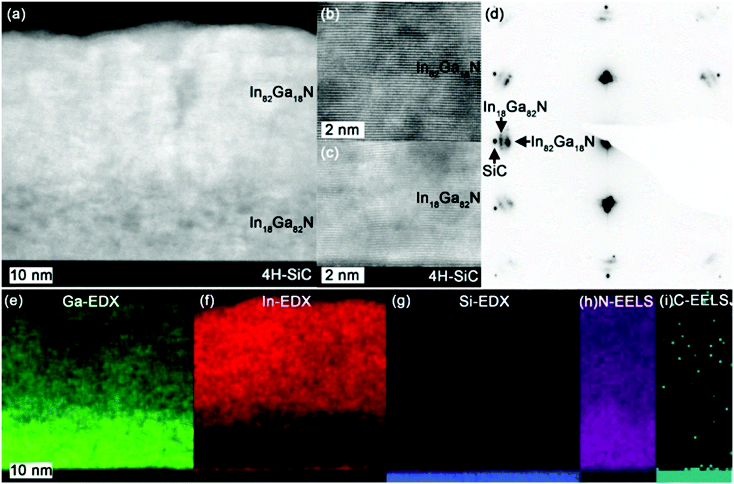 | ||
| Fig. 2 (a) Cross-sectional STEM-HAADF image of the ∼60 nm In1−xGaxN film on the 4H–SiC substrate with a zoomed in image of the (b) In82Ga18N and (c) In18Ga82N layers. (d) SAED pattern from the film and substrate. EDX maps of Ga (e), In (f) and Si (g). EELS maps of N (h) and C (i). | ||
A Tauc-plot was constructed from an absorption measurement for an In1−xGaxN film deposited on Si(100) at 350 °C with the metal precursors mixed in a 1:1 ratio and sublimed at 150 °C. The linear part of the plot was extrapolated down to the x-axis and a bandgap of approximately 1.94 eV was obtained for the In1−xGaxN film (Fig. 3). The XPS measurements showed the film composition was In0.55Ga0.45N (Table S1, ESI†), which should result in a band gap value of 1.92 eV from Vegard's law (eqn (1)).
| Eg(InxGa1−xN) = X*Eg(InN) + (1 − X)Eg(GaN) | (1) |
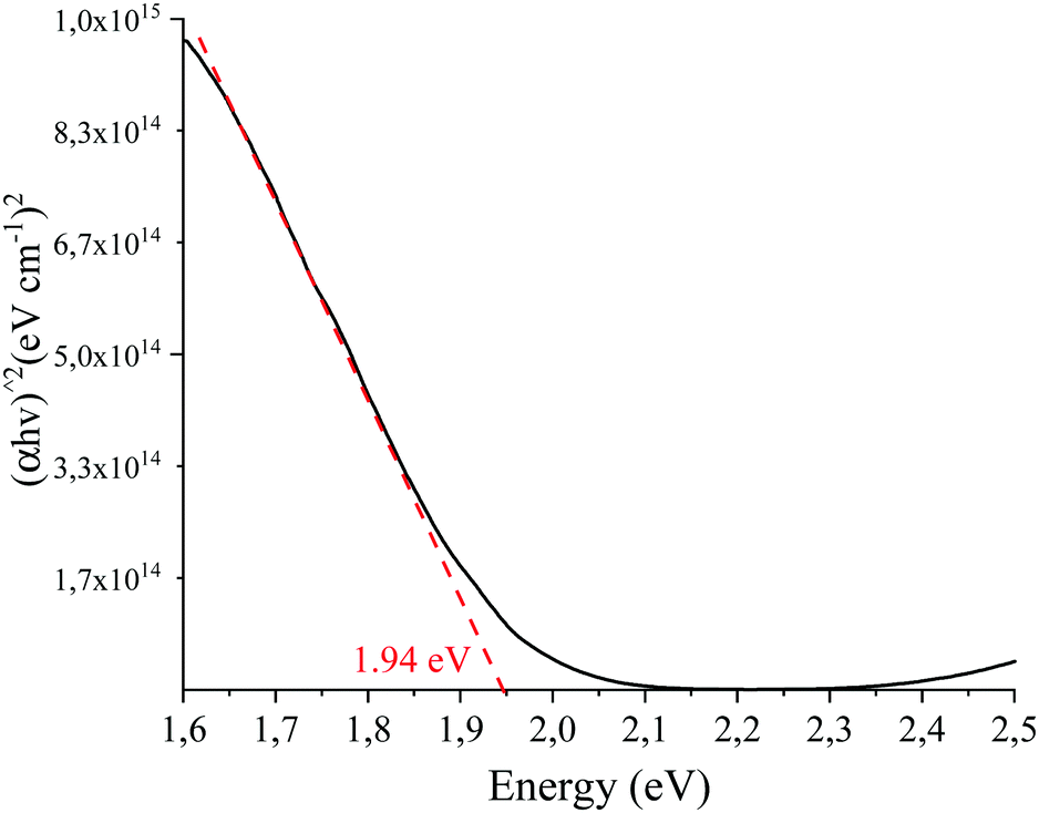 | ||
| Fig. 3 Tauc-plot from absorption measurement of 60 nm thick In55Ga45N analyzed with XPS deposited at 350 °C on a Si(100) substrate. | ||
This value correlates well with the experimental bandgap obtained from the absorption measurements. Top-view scanning electron microscope (SEM) images showed a smooth film with evenly distributed grain size (Fig. S7, ESI†). No signs of in metal droplets were observed, suggesting that the deposited In1−xGaxN is in a single ternary phase. The presence of In metal droplets on the surface is otherwise a clear indication of decomposition of the ternary In1−xGaxN phase.8
Conclusions
In summary, we have developed a new ALD approach for ternary materials based on co-sublimation of the metal precursors as an alternative to the super-cycle approach. This method was employed to deposit In1−xGaxN by mixing Ga(III) and In(III) triazenides, co-subliming them and using NH3 plasma as the N-reactant. In1−xGaxN was successfully deposited on Si(100) and 4H–SiC(0001) without the need of a seed layer. It was found the composition of the In1−xGaxN could be tuned by changing the sublimation- and deposition temperatures, and the ratio of the two metal precursors. An In1−xGaxN film with a near 1:1 ratio between the metals was confirmed using XPS, RBS, ToF-ERDA and absorption measurement of the bandgap. The In1−xGaxN film grew epitaxially on 4H–SiC(0001) without phase segregation or decomposition of the In1−xGaxN into the binary materials or In droplets. A composition gradient was revealed with a more Ga-rich composition near the substrate/film interface and more In-rich composition near the top of the film. This was presumably due to stress minimization as the lattice mismatch is smaller for Ga-rich InGaN compared to In-rich InGaN or the deposition behavior of the metal precursors on the surface. We believe that this co-sublimation method could be applied to various material systems where the metal precursors have overlapping sublimation- and ALD temperatures. We foresee that it could also be utilized for doping.
Conflicts of interest
PR and HP have applied for a patent on this method.Acknowledgements
P. R. acknowledges Erik Martinsson for the assistance with the absorption measurements. This project was funded by the Swedish Foundation for Strategic Research through the project “Time-resolved low temperature CVD for III-nitrides” (SSF-RMA 15-0018) and by the Knut and Alice Wallenberg Foundation through the project “Bridging the THz gap” (No. KAW 2013.0049). Support from the Swedish research council VR-RFI (2017-00646_9) for the Accelerator based ion-technological center, and from the Swedish Foundation for Strategic Research (RIF14-0053) for the tandem accelerator laboratory in Uppsala is gratefully acknowledged. The authors acknowledge the Knut and Alice Wallenberg Foundation for support of the electron microscopy laboratory in Linköping and a project grant (KAW 2020.0033).References
- J. Li, K. B. Nam, M. L. Nakarmi, J. Y. Lin, H. X. Jiang, P. Carrier and S. H. Wei, Appl. Phys. Lett., 2003, 83, 5163–5165 CrossRef CAS.
- Y. C. Tsai and C. Bayram, Sci. Rep., 2019, 9, 1–9 Search PubMed.
- M. Gopalakrishnan, V. Purushothaman, P. S. Venkatesh, V. Ramakrishnan and K. Jeganathan, Mater. Res. Bull., 2012, 47, 3323–3329 CrossRef CAS.
- M. A. H. Howlader, A. K. Saha, M. S. Hasan and M. R. Islam, Proc. 2014 3rd Int. Conf. Dev. Renew. Energy Technol. ICDRET 2014, 4–8.
- I. H. Ho and G. B. Stringfellow, Mater. Res. Soc. Symp. Proc., 1997, 449, 871–880 CrossRef CAS.
- S. V. Ivanov, T. V. Shubina, T. A. Komissarova and V. N. Jmerik, J. Cryst. Growth, 2014, 403, 83–89 CrossRef CAS.
- H. Matsuura, T. Onuma, M. Sumiya and T. Yamaguchi, Appl. Sci., 2019, 9, 1–8 Search PubMed.
- H. Hartono, S. J. Chua, E. A. Fitzgerald, T. L. Song and P. Chen, Mater. Res., 2005, 1–4 Search PubMed.
- S. Surender, K. Prabakaran, R. Loganathan, S. Pradeep, S. Singh and K. Baskar, J. Cryst. Growth, 2017, 468, 249–251 CrossRef CAS.
- Y. Huang, J. Photonics Energy, 2012, 2, 028501 CrossRef.
- K. Rönnby, H. Pedersen and L. Ojamäe, J. Vac. Sci. Technol., A, 2020, 38, 050402 CrossRef.
- N. J. O’Brien, P. Rouf, R. Samii, K. Rönnby, S. C. Buttera, C. W. Hsu, I. G. Ivanov, V. Kessler, L. Ojamäe and H. Pedersen, Chem. Mater., 2020, 32, 4481–4489 CrossRef.
- N. Nepal, V. R. Anderson, J. K. Hite and C. R. Eddy, Thin Solid Films, 2015, 589, 47–51 CrossRef CAS.
- S. Consiglio, K. Tapily, R. D. Clark, G. Nakamura, C. S. Wajda and G. J. Leusink, J. Vac. Sci. Technol., A, 2013, 31, 01A115 CrossRef.
- H. Yuan, B. Luo, D. Yu, A. Cheng, S. A. Campbell and W. L. Gladfelter, J. Vac. Sci. Technol., A, 2012, 30, 01A138 CrossRef.
- A. Illiberi, R. Scherpenborg, Y. Wu, F. Roozeboom and P. Poodt, ACS Appl. Mater. Interfaces, 2013, 5, 13124–13128 CrossRef CAS PubMed.
- P. Rouf, R. Samii, K. Rönnby, B. Bakhit, S. C. Buttera, I. Martinovic, L. Ojamäe, C. W. Hsu, J. Palisaitis, V. Kessler, H. Pedersen and N. J. O’Brien, Chem. Mater., 2021, 33, 3266–3275 CrossRef CAS.
- M. Stockmeier, R. Müller, S. A. Sakwe, P. J. Wellmann and A. Magerl, J. Appl. Phys., 2009, 105, 033511 CrossRef.
- S. Strite, J. Vac. Sci. Technol., B: Microelectron. Nanometer Struct.--Process., Meas., Phenom., 1992, 10, 1237 CrossRef CAS.
Footnote |
| † Electronic supplementary information (ESI) available. See DOI: 10.1039/d1tc02408f |
| This journal is © The Royal Society of Chemistry 2021 |