
 Open Access Article
 This Open Access Article is licensed under a
 Creative Commons Attribution 3.0 Unported Licence
Reactive inkjet printing of graphene based flexible circuits and radio frequency antennas†
Songwei
Lv‡
a,
Siyuan
Ye‡
a,
Chunling
Chen
b,
Yi
Zhang
c,
Yanhong
Wu
d,
Yiqing
Wang
a,
Runli
Tang
d,
M. M.
De Souza
 e,
Xuqing
Liu
f and
Xiubo
Zhao
*ac
e,
Xuqing
Liu
f and
Xiubo
Zhao
*ac
aSchool of Pharmacy, Changzhou University, Changzhou 213164, China. E-mail: xiubo.zhao@cczu.edu.cn
bSchool of Microelectronics and Control Engineering, Changzhou University, Changzhou 213164, China
cDepartment of Chemical and Biological Engineering, University of Sheffield, Sheffield S1 3JD, UK
dThe Sixth Element (Changzhou) Materials Technology Co., Ltd, Changzhou 213164, China
eDepartment of Electronic and Electrical Engineering, University of Sheffield, Sheffield S3 7HQ, UK
fDepartment of Materials, University of Manchester, Manchester M13 9PL, UK
First published on 5th August 2021
Abstract
Graphene-based materials show great promise in wearable electronics due to their remarkable properties such as excellent electrical conductivity, high flexibility and light weight. Various techniques have been used to fabricate graphene-based electronics, such as lithography, template-assisted synthesis, and chemical vapor deposition. However, these patterning methods normally involve complex procedures, toxic solvents and extra machinery, which are highly challenging for large-scale industrial production. Herein, we have developed an in situ approach to fabricate reduced graphene oxide (rGO) conductive patterns on flexible substrates via reactive inkjet printing without any post-treatment. Electronic circuits and WIFI antennas consisting of conductive rGO lines with a minimum width of 100 μm and remarkable mechanical durability were successfully fabricated. The highest electrical conductivity of the printed rGO lines was 2.69 × 10⁴ S m−1 using optimised printing conditions. The rGO based radio frequency antenna demonstrated transmission with a measured domain name system (DNS) delay of 243 ms. When accessed via a 100 Mbps router, the network speed reached up to 4.64 Mbps, which is comparable to that of the current commercial mobile phone antenna (DNS delay 237 ms, network speed 4.73 Mbps). This demonstrates the potential of reactive inkjet printing for the industrialisation of graphene-based wearable electronics.
1 Introduction
The Internet of Things (IoT), connecting hardware to the internet, dramatically improves our work and life. Wireless communication sensors such as flexible radio-frequency identification (RFID) antennas are essential components enabling information exchange for IoT.1–5 Currently, antenna materials are mainly based on metals, such as aluminium, copper and silver, which possess excellent electrical conductivity.2 However, two critical problems remain to be addressed for a wider spectrum, and higher frequency: (1) With an increase in frequency, the resistance of the metal surface increases sharply, which causes a dramatic decrease in the magnitude of the electromagnetic wave propagated on the metal surface and is called the skin effect.3,6–8 (2) With miniaturization of antennas, it becomes tremendously challenging to fabricate using printed circuit board (PCB) technology.9–11High-resolution patterning is one of the key processes for fabricating flexible electronics.12–15 However, several commonly used techniques for device fabrication including lithography,16 template-assisted synthesis,17 and chemical vapor deposition (CVD)18 usually require complex multi-step procedures that are often incompatible with the fabrication of antennas that have dimensions much larger than those of present day CMOS devices. This usually results in the integration of the antenna either in the package or as a separate component mounted via the PCB. By contrast, inkjet printing shows advantages of fast deposition, high resolution, and precise control of deposited materials in terms of quantity and location, simplified operating procedures and non-contact direct printing; therefore, it has gained popularity in flexible applications of electronic devices.5,14,19–25 Metallic nanoparticles such as gold, silver and copper are widely used as inks for inkjet mainly owing to their paramount electrical conductivity. However, there are several disadvantages of using these inks to fabricate flexible electronics: (1) Stabilising agents are normally required to avoid agglomeration of metal nanoparticles dispersed in inks, which is detrimental to the electrical conductivity of printed features; (2) The post-annealing step commonly requires a high temperature which is harmful to most wearable substrates such as textiles; (3) Gold and silver nanoparticles are expensive; and (4) Copper is easily oxidised when exposed to an ambient environment, which results in a short life-time of the fabricated electronics.26–28
Graphene and its derivatives, such as graphene oxide (GO) and reduced graphene oxide (rGO), show great promise in flexible electronics on account of their excellent chemical and environmental stability, mechanical flexibility and electrical conductivity.6,29–33 It has been recently shown that the lateral confinement of electrons in semi-finite-size graphene nanoribbons (GNRs) enhances the material conductivity even up to the terahertz band.34,35 Moreover, compared with other conductive materials (such as metal nanowires and metallic nanoparticles), graphene materials can overcome the skin effect of existing materials.6 However, most of the current graphene patterning is based on graphene inks (including reduced graphene or mechanically exfoliated graphene).19,20,36–40 Stabilization agents are commonly required to obtain printable graphene-based inks as graphene is insoluble in water. Unfortunately, the addition of stabilization agents is detrimental to the electrical conductivity of the printed tracks. Moreover, the inherently plicated graphene sheets are hard to stack compactly due to van der Waals forces. Thus, the electronic conductivity is compromised.19,36–38 On the other hand, GO shows good stacking properties because of its self-assembling capability.41–43 GO films prepared from GO suspension are insulating, but can be reduced to form dense graphene films, which show exceptional conductivity.44,45 Despite the GO suspension being readily patternable, which makes it an ideal water-based printing ink, there are few reports on highly conductive graphene using GO-based inkjet printing.46 The main obstacle is an insufficient reduction process after the GO printing.30,47–53 In order to improve the overall degree of reduction of the printed material, Su et al. used a “weak oxidation–vigorous exfoliation” strategy to reduce the defects of GO and thus to reduce the difficulty of subsequent reduction. However, an inherent problem with this approach is that weakly oxidized GO may not be efficiently dispersed and assembled.53
Our previous work demonstrated that the in situ formation of unprintable materials through reactive inkjet printing (RIJ) was achieved by alternative printing of two reactive components on top of each other to trigger the reaction and form the product.54,55 Herein, we developed an encouraging in situ approach that combines patterning and in situ reduction using RIJ. Briefly, the GO suspension (ink-A) and the reducing agent (ink-B) were alternately deposited in a “sandwich configuration”, resulting in in situ patterning and reduction (Fig. 1 and Video S1, ESI†). Owing to the self-assembly of GO and precise control of chemical reduction, a high conductivity (2.69 × 10⁴ S m−1) of the graphene pattern was successfully achieved. In addition, we applied this technique to fabricate graphene radio frequency (RF) antennas for different frequency bands. The echo loss and gain of 2.4 G smartphones were found at a DNS latency of 243 ms and a network speed of 4.64 million bits per second (Mbps), comparable to current commercial mobile phone antennas (237 ms and 5 Mbps). This approach combines the advantages of both reactive inkjet printing and graphene-based materials, and facilitates the fast and cost-effective fabrication of antennas. In addition, it provides an on-demand facile integration of graphene into various flexible substrates and electronic devices.
 | ||
| Fig. 1 A schematic illustration of the in situ approach combining patterning and in situ reduction of GO patterns using reactive inkjet printing. | ||
2 Materials and methods
2.1 Materials
All reagents were of analytical grade from commercial sources and used without further purification. GO was obtained from The Sixth Element (Changzhou) Materials Technology Co., Ltd. China. Hydroiodic acid (HI, 45%) and anhydrous ethanol were purchased from Sinopharm Chemical Reagent Co., Ltd. Polyethylene terephthalate (PET) films were used as substrates for inkjet printing. Deionized (DI) water (Elga LabWater Chorus Complete) with a resistivity of 18.2 MΩ was used in all experiments.2.2 Ink preparation
GO solution was diluted to a concentration of 1% using DI water. A 10 μm nylon filter membrane was used in a Brinell funnel to filter the solution thrice. The filtered solution was sonicated in a water bath (RT) for 2 hours to obtain GO ink (ink-A). The reductant ink (ink-B) was prepared with diluted hydroiodic acid.2.3 Plasma treatment of the PET substrate
In order to improve the wettability of the substrate, the PET films were firstly cleaned with anhydrous ethanol followed by oxygen plasma treatment (CIF CPC-B-13.56) at 80 W for 90 seconds.2.4 Reactive inkjet printing process
Printheads with 80 μm nozzle diameter were used for printing. Reactive inkjet printing was performed using a piezoelectric drop-on-demand (DOD) inkjet printer (Jetlab4xl-A, MicroFab) with a resolution of 5 μm in the XY directions. The volume of ejected droplets ranged between 50 and 150 pL. Ink-A (GO suspension) and Ink-B (HI solution) were alternatively printed on the PET substrate, which was heated to 50 or 70 °C to accelerate the evaporation of the water. Except for the humidity test, all electrical performance and mechanical performance measurements were performed at 50% humidity.2.5 Fabrication of a RFID antenna and WIFI antenna
The dipole antenna and 2.4 G WIFI antenna were designed by using CAD drawing software. The fabrication processes were as follows: 20 layers of GO ink were printed according to the designed antenna pattern followed by the printing of 3 layers of 45% HI after the complete drying of the printed GO pattern. During printing, the platform was heated to 70 °C to ensure the full reduction of GO. The antenna was dried overnight at room temperature in a vacuum oven.2.6 Characterization
The size of the GO sheets was measured by Dynamic Light Scattering (DLS, Malvern Nano ZSE). The viscosities of inks were measured using a viscometer (Brookfield DV-II+ Pro). The wettability of the inks/substrates was evaluated by measuring their contact angles (Kruss GmbH FM4000). The transmittance of the printed GO and rGO films was determined using an ultraviolet–visible spectrophotometer (TU-1810, PERSEE). Infrared spectra of GO and rGO were measured using a Fourier Transform Infrared spectrometer (FTIR, Bruker VERTE X70). The crystal structures of GO and rGO were analysed using an X-Ray Diffractometer (XRD, Rigaku, Smart lab 9). The degree of reduction of GO was analysed using a Raman spectrometer (Thermo Fisher DXR 3xi). X-Ray Photoelectron Spectroscopy (XPS, Thermo Fisher Nexsa) was used to analyse the elemental change of oxygen-containing groups before and after the reduction of GO. Morphological and structural information was analysed using a Scanning Electron Microscope (SEM, SUPRA55) and an Atomic Force Microscope (AFM, JPK Nanowizard 4). The conductivity of the rGO pattern was measured using a four-probe resistance meter (Helpass Electronic Technologies Inc.). The thickness of rGO patterns was determined using a step meter (DektakxT DXT-18-1821). The radiation characteristics of the antenna were characterised using a spectrum analyser (Agilent Technologies E5071C).3 Results and discussion
3.1 Characterization of the inks and substrates
The AFM image (Fig. 2a) and the DLS analysis (Fig. 2b) indicated that the GO flake size was around 3 μm. Although the size and polydispersity of GO inks increased after 3 months of storage, they still showed excellent printability (Fig. S1, ESI†). | ||
| Fig. 2 Characterization and printability of GO ink. (a) A representative AFM image of GO sheets in GO ink. (b) Particle size and PDI of the GO ink. (c) Contact angles for a droplet of the GO ink and a droplet of the HI ink on PET before and after plasma treatment. Upper: GO ink; lower: HI ink. (d) Printed rGO lines with different widths, from left to right 1, 0.5, 0.3, and 0.1 mm, respectively. (e) The enlarged image of the 0.1 mm line. (f and g) Comparison of printed patterns before and after reduction through reactive inkjet printing. (f) GO pattern and (g) rGO pattern. | ||
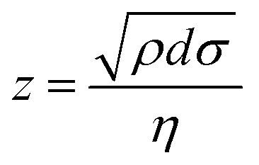
The wettability of the substrate affects the printing resolution via droplet spreading on substrates. In order to ensure the consistent wettability of the substrate, the PET film was treated with oxygen plasma to improve its hydrophilicity. The contact angles of the GO ink on the untreated and treated substrates were 55.2° and 26.0°, respectively (Fig. 2c). The contact angles of the HI ink on the untreated and treated substrates were 29.7° and 16.5°, respectively (Fig. 2c). Therefore, the decrease in the contact angle indicates an improvement in the wettability of the substrate. In inkjet printing, surface tension and viscosity play a crucial role in the performance of the ejected droplet, which significantly affects the printability of an ink. Normally, inks with surface tension ranging from 28 mN m−1 to 350 mN m−1 and viscosity < 20 cP are accepted as printable inks. Highly viscose inks cannot be ejected to form a stable droplet stream for printing. The dimensionless number, i.e., the Z number which is derived from surface tension and viscosity is commonly used to predict droplet formation. It has been reported that inks with 1 < Z < 10 are suitable for inkjet printing (Eqn 1).56
 | (1) |
3.2 The characterisation of printed GO patterns
Inkjet printed line widths are one of the basic patterns that reflect the printing resolution of conductive lines.57Fig. 2d shows lines with different widths, inkjet printed on PET substrates. The lengths are 25 mm and the widths are 1, 0.5, 0.3, and 0.1 mm, respectively. In this work, the minimum width of a single-droplet line printed on the plasma treated PET film was approximately 100 μm (Fig. 2e and Fig. S3, ESI†). The relationship between the number of printed layers and the thickness of the printed pattern was characterised. It was revealed that the thickness of the printed pattern had a linear relationship with the number of printed layers (Fig. S4, ESI†). The thickness of the first layer was approximately 105 nm, and the thickness increased by approximately 18–25 nm per layer. The University logo was patterned by RIJ (Fig. 2f and g) to demonstrate the capabilities of 2D patterning and in situ reduction (from GO (brown) to rGO (black)) of the RIJ technology.3.3 Optimization of reactive inkjet printing conditions
The self-assembly performance and degree of reduction of GO are affected by whether a drying step is included between each printed layer or not. The XRD results showed that the peak width at half maximum of printing with drying intervals is smaller than that of printing without drying intervals, indicating the better self-assembly and uniformity of the former (Fig. 3a). This may be due to the fact that the evaporation of liquid (gradually reduced volume) facilitates the self-assembly of GO sheets.42 Therefore, the resultant structure of printing with drying intervals has more self-assembled layers than that of printing without drying intervals. | ||
| Fig. 3 Chemical and morphological characterization. (a) XRD of rGO patterns printed with and without drying intervals. (b) Raman spectra of rGO reduced at different HI concentrations and their corresponding ID/IG values. The decrease in ID/IG values indicates the improved reduction of GO. (c) Infrared spectra of GO and rGO prepared under optimal conditions (45% HI, 20 layers of GO, 3 layers of HI, substrate temperature 70 °C). (d) XRD of printed GO and rGO. (e and f) XPS spectra (C1s) of GO and rGO clearly showed that the characteristic peaks of the oxygen-containing groups of rGO were weakened (f). (g and h) SEM images of the morphology of GO and rGO patterns printed with drying intervals (0.5 mg mL−1 GO ink, 45% HI ink was used to print 20 layers of GO, 3 HI layers at a base plate temperature of 70 °C). The surface of the rGO pattern was smoother than that of the GO pattern. (i and j) SEM images of the cross-sections of printed GO and rGO patterns (100 layers of GO). Both GO and rGO patterns had similar laminar structures. | ||
The degree of GO reduction is affected by three factors: (i) concentration of the HI ink, (ii) number of printed GO layers and (iii) the temperature of the substrate. Raman spectroscopy revealed that with an increase of HI concentration, the ratio of the peak intensity of the ID/IG band gradually decreased from 1.675 to 1.286 (Fig. 3b), indicating a decrease of the disordered carbonaceous structure due to increased reduction of oxygen containing groups. The peak values of oxygen-containing groups are 1630 cm−1, 1396 cm−1 and 1052 cm−1, attributed to C![[double bond, length as m-dash]](https://www.rsc.org/images/entities/char_e001.gif) O (the bending vibration of water molecules), C–OH and C–O, respectively, as seen in the IR spectrum in Fig. 3c.58 Less branched groups hinder the formation of the ordered graphitic structure as shown in Fig. 3d. It can be seen that the 2θ of rGO is 26.31° and the interlayer spacing is 3.67 Å, very close to that of natural graphite. On the other hand, the 2θ of GO is 11.85°, and the interlayer spacing is 7.34 Å. The reduced interlayer spacing is due to the removal of oxygen-containing functional groups after reduction. Fig. 3e and f show the C1s XPS spectra of GO and rGO, indicating the noticeable enhancement of the C–C/CC bond (aromatic rings) and a reduced intensity of oxygen-containing groups after reduction.59 Fig. S5 (ESI†) shows a significant decrease in the opacity of the rGO film compared to the GO film.
O (the bending vibration of water molecules), C–OH and C–O, respectively, as seen in the IR spectrum in Fig. 3c.58 Less branched groups hinder the formation of the ordered graphitic structure as shown in Fig. 3d. It can be seen that the 2θ of rGO is 26.31° and the interlayer spacing is 3.67 Å, very close to that of natural graphite. On the other hand, the 2θ of GO is 11.85°, and the interlayer spacing is 7.34 Å. The reduced interlayer spacing is due to the removal of oxygen-containing functional groups after reduction. Fig. 3e and f show the C1s XPS spectra of GO and rGO, indicating the noticeable enhancement of the C–C/CC bond (aromatic rings) and a reduced intensity of oxygen-containing groups after reduction.59 Fig. S5 (ESI†) shows a significant decrease in the opacity of the rGO film compared to the GO film.
The morphology of printed GO and rGO lines is shown in Fig. 3g and h. The surface of the printed GO pattern has many “ridges”. The ridges were produced by the evaporation of the solvents after GO droplets deposited on the substrate. During this process, GO sheets were carried by droplet shrinking due to solvent vaporizing, forming ridges. When GO was exposed to HI, a large number of oxygen-containing functional groups were removed by reduction, resulting in well-ordered rGO sheets, reflected by the flattening of the “ridge” surface,60 which improved the electrical conductivity. Fig. S6a (ESI†) presents the optical micrograph of printed GO droplets under an AFM probe, and Fig. S6b (ESI†) shows an AFM image at the edge of a circular droplet. The cobwebs in this image are similar to the “ridges” in SEM. Due to the shear deformation during the preparation process of the 20 layer rGO cross section, the 100 layer rGO cross section was used as the representative for characterization. Fig. 3i and j show the laminar structure of the cross-sections of both GO and rGO patterns (100 layers). The SEM images show that the rGO films stack like paper sheets in a book, and the gap between the layers clearly testifies the remarkable well-ordered self-assembly of the rGO layers.
The degree of reduction of GO affects the electrical conductivity of the final rGO patterns. Fig. 4a shows that the conductivity of the rGO patterns increases with the number of layers for a fixed HI concentration, and the increase of HI concentration until 30%. With an increase of printed GO layers or substrate temperature, their orientation improves, resulting in a smaller ratio of the intensity of ID/IG bands, higher conductivity and darker films (Fig. S7 and S8, ESI†). To investigate the reason for the rapid increase of the electrical conductivity of 20–30 layers, Raman and X-ray diffraction spectra were used to study the apparent in-plane crystallite size (La) and apparent crystallite size in the c direction (Lc) of the 20 and 30 layers, respectively.61 As displayed in Table S1 (ESI†), with an increase of printed rGO layers, the Lc value increased from 6.36 nm to 10.41 nm. The increase of longitudinal grain size leads to a sharp increase in the electrical conductivity of rGO films. On the other hand, the conductivity of rGO patterns gradually increases with HI layers (Fig. 4b). However, beyond 3 HI layers irregular HI residues are formed on the surface of the GO pattern. Although there is no significant influence of temperature on the reduction between 25 °C and 50 °C, beyond 70 °C, the conductivity is slightly elevated as shown in Fig. 4c.
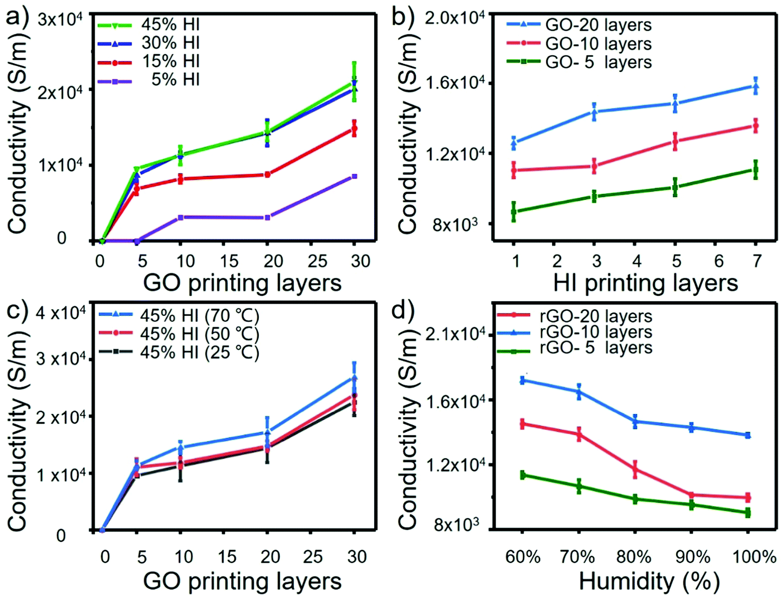 | ||
| Fig. 4 Electrical conductivity tests. (a) The conductivity of the printed rGO patterns using different concentrations of HI inks (the number of printed HI layers was 3) and different layers of GO inks. (b) The conductivity of the rGO film formed by printing different HI layers on different GO layers, where the HI concentration is fixed at 45%. (c) The influence of different heating temperatures on the conductivity of rGO during the inkjet reduction process. (d) Resistivity variation of rGO with different layers under different humidity under in situ reduction conditions. | ||
In summary, with intermittent drying between each layer, 0.5 mg mL−1 GO ink, 45% HI ink was used to print 30 layers of GO, 3 HI layers at a base plate temperature of 70 °C, to yield the maximum conductivity (2.69 × 10⁴ S m−1) of the rGO film. By studying the resistivity changes of rGO under different humidity conditions (the humidity conditions in this experiment ranged from 50% to 100%), the rGO can also be used as a humidity sensor (Fig. 4d).
3.4 Electrical conductivity and mechanical durability of rGO patterns
The rGO line was printed on a plasma-treated PET film, then a conductive copper glue was used to connect the rGO line with a LED light strip (Fig. 5a and b). Fig. 5c demonstrates the conductivity of the printed rGO line. Aiming for flexible electronic devices, the entire conductive circuit was bent to test the flexibility of the printed rGO lines (Fig. 5d). It was found that the brightness of the LED light strip was not affected by the bending of the substrate (ESI,† Video S2). | ||
Fig. 5 Conductivity and mechanical durability tests of the printed rGO circuit. (a) A circuit consisting of a LED strip and a rGO line which was prepared by reactive inkjet printing. (b) The rGO line and the LED strip were connected using conductive copper glue. (c) The demonstration of the conductivity of the printed rGO line (power: DC 5 V). (d) The whole circuit was subjected to bending as shown. (e–h) The absolute and relative electrical resistance changes of rGO lines (5, 10, 20 and 30 layers) along with inward and outward bending cycles show degradation of 25% to the resistance due to bending. (i–l) SEM images of the morphology of the printed 20 layers rGO lines before and after 10![[thin space (1/6-em)]](https://www.rsc.org/images/entities/char_2009.gif) 000 cycles of inward and outward bending. 000 cycles of inward and outward bending. | ||
The mechanical durability was tested by a large number of cyclic mechanical deformations, i.e., inward and outward bending (ESI,† Video S3). Fig. 5e and g show that the absolute resistance slightly increases with the cycle number. The mechanical durability of the printed rGO features in this study was compared with previously reported works (Table 1).46,62–67 After 2000 cycles of inward or outward bending, there is no measurable change in resistance (<3%). The change of relative resistance after 10000 cycles was up to 50% and 30% of inward and outward bending, respectively (Fig. 5f and h). The SEM images show the surface morphology of the printed rGO lines before and after 10000 cycles of mechanical deformations (Fig. 5i–l). In Fig. S9 and Table S2 (ESI†), we conducted quantitative statistics on the crease density and width after bending. The results show that bending has no obvious effect on crease width, but the crease density increased significantly after 10000 cycles of inward bending. The main reason for the increase of resistance after bending may be the increase in crease density. The electrical conductivity of the substrate after bending can be improved by using substrate materials with better bending performance, such as PDMS, or by pre-stretching the patterned surface of the substrate.
| Ink type | Deposition | Substrate | Curing | Sheet resistance (Ω □−1) | Resistivity (Ω m) | ΔR/R bending cycles | Ref. |
|---|---|---|---|---|---|---|---|
| GO ink | Inkjet | PET | 70 °C | 53.3 | 4.26 × 10⁻⁵ | 2000 | This work (30 layers) |
| GO ink | Inkjet | Bare glass | 80 °C | 1.08 × 10⁵ | 3.88 × 10⁻² | — | 46 |
| Graphene ink | Transfer | PET | ∼250 °C | 470 ± 80 | 1.5 × 10⁻³ | 1000 | 62 |
| Graphene ink | Screen-Printing | Polyimide | 350 °C | 15 ± 2 | 1.14 × 10⁻⁵ | 1000 | 63 |
| Graphene ink | Polymer casting | Polyimide | Room temperature | 200 ± 3 | — | 100 | 64 |
| Graphene-nitrocellulose | Aerosol-jet | Polyimide | 350 °C | 33.3 | 1.5 × 10⁻⁴ | 1000 | 65 |
| Graphene ink | Inkjet | Bare glass | 396.85 °C (670 K) | 300 ± 5 | 1 × 10⁻⁴ | — | 66 |
| Graphene ink | Inkjet | Si/SiO2 | 250 °C | 148 | 2 × 10⁻⁵ | — | 67 |
3.5 Preparation of a dipole antenna
In the application of a dipole antenna, the length and width of a single antenna are 15 cm and 0.5 cm, so the printing time significantly increased between 20 layers and 30 layers. In addition, the conductivity of 20 and 30 layers of rGO can both meet the requirements of antenna performance (20 layer 1.69 × 10⁴ S m−1; 30 layer 2.69 × 10⁴ S m−1). Considering the time and the basic performance of the antenna, we chose 20 layers for the antenna experiment. A dipole antenna was designed using the Finite Element Method (FEM)-based full-wave simulator (Ansoft HFSS). The configuration and prototype of the dipole antenna are shown in Fig. 6a. The antenna consists of two arms with a gap of 2 mm. The dimension of each arm was designed to be 75 × 5 mm to resonate at 840 MHz. The current distributions were calculated using commercial software ANSYS HFSS 18.0 which solves Maxwell's equations by the finite element method. The current flow in one period is shown in the animation (Fig. S10, ESI†). In addition, the magnitude of the current near the centre is stronger than that at the two ends. The direction of the current remains unchanged along the strip. Therefore, it is a half-wavelength dipole antenna. The rGO line was printed on a dielectric laminate with a permittivity of 2.2 and a thickness of 1.6 mm. A 50 Ω coaxial cable was utilized to feed the antenna without using balanced designs. It is noted that in applications where the antenna is used inside the circuit of a complete system, the need for the balun is automatically eliminated. Fig. 6b compares the simulated and measured |S11|, showing a measured null at 864 MHz, which is only 3% higher than that of the simulation due to the fabrication tolerance. The measured gain of the antenna was 0.64–1.5 dB less than that of a traditional half-wavelength dipole antenna. It should be noted that a perfect conductor is assumed in the simulation. However, the conductivity of the printed rGO lines is 1.69 × 10⁴ S m−1 (20 layers) which causes an Ohmic loss. | ||
| Fig. 6 Printed rGO dipole antenna. (a) A schematic of dipole antenna design and a printed antenna. The antenna and feeder were connected with a conductive copper glue. (b) The red and black lines represented the simulated and measured resonance peaks (|S11|) of the dipole antenna, respectively. (c) The simulated and measured E-plane pattern of the dipole antenna. (d) The simulated and measured diagram of the H-plane pattern of the dipole antenna. (e) Actual scene of the E-plane pattern of a dipole antenna. (f) Actual scene of the H-plane pattern of a dipole antenna. | ||
The measured and simulated radiation patterns in the xoy-plane (E-plane) and yoz-plane (H-plane) are presented in Fig. 6c and d, which show good agreement between simulation and measurement. Moreover, the levels of the cross-polarization in the E-plane and H-plane are less than −20 dB and −10 dB, respectively. The antenna demonstrates omnidirectional radiation, which makes it suitable for a mobile communication system with randomly oriented terminals.
In order to verify that the rGO antenna is fully compatible and functional in smart mobile phones, a 2.4 G WIFI antenna was designed in rGO to replace the original WIFI antenna in a smartphone (Fig. 7a–d). Here, an inverted F-shaped antenna is designed as shown in Fig. 7a in blue and measured. On the other hand, we use a copper sheet (yellow part) to represent the smartphone. A vector network analyser is utilized to measure the antenna. The result in Fig. 7b reveals that the |S11| is less than −10 dbB from 2.0 GHz to 2.9 GHz, which covers the entire WIFI band (2.4–2.483 GHz). Through commercial software, the DNS delay of 243 ms was measured after access to a 100 Mbps router, which enables a network speed of up to 4.64 Mbps. The performance was comparable to the current commercial mobile phone antenna (DNS delay 237 ms, network speed 4.73 Mbps) (Fig. 7e, f and ESI,† Video S4). This preliminary result is an excellent demonstration of the rGO antenna fabricated by in situ reactive inkjet printing for wireless communication, indicating its promising potential in wearable electronics.
 | ||
| Fig. 7 Printed mobile phone WIFI antenna. (a) A schematic of 2.4 G antenna design. (b) The measured resonance peaks (|S11|) of the 2.4 G antenna. (c) rGO antenna was connected to a smartphone WIFI contact. (d) Smartphone WIFI signal was restored after connecting to the rGO antenna. (e and f) Performance comparisons between the mobile phone built-in antenna and rGO antenna, including DNS latency, network latency, and network speed testing. | ||
4 Conclusions
In conclusion, we developed a simple and effective strategy to fabricate rGO patterns on flexible substrates through reactive inkjet printing. By controlling the reaction conditions and printing methods to control the degree of reduction and self-assembly of GO, highly conductive rGO patterns were obtained. Smooth conductive lines with a resolution of 100 μm were printed on the plasma-treated PET films. The highest electrical conductivity of the printed rGO lines was 2.69 × 10⁴ S m−1. In addition, the printed rGO patterns possess excellent mechanical durability, suitable for flexible electronic devices. Furthermore, we applied this approach to fabricate a mobile phone WIFI antenna with a measured DNS delay of 243 ms after access to a 100 Mbps router enabling a measured network speed of 4.64 Mbps. The performance of the fabricated antenna is comparable to that of a commercial mobile phone antenna. It is worth noting that through reactive inkjet printing, electronic patterns of any shape (such as electronic circuits, antennas, RFID tags and sensors) can be fabricated for wireless wearables. The current work demonstrates that reactive inkjet printing is a promising technology for the fabrication of graphene-based flexible electronics.Conflicts of interest
The authors declare that there are no competing interests.Acknowledgements
The authors would like to acknowledge the Jiangsu specially appointed professor program and EPSRC (EP/N007174/1 and EP/N023579/1) for support.References
- R. A. Potyrailo, Multivariable Sensors for Ubiquitous Monitoring of Gases in the Era of Internet of Things and Industrial Internet, Chem. Rev., 2016, 116(19), 11877–11923 CrossRef CAS PubMed.
- A. Sarycheva, A. Polemi, Y. Liu, K. Dandekar, B. Anasori and Y. Gogotsi, 2D titanium carbide (MXene) for wireless communication, Sci. Adv., 2018, 4(9), eaau0920 CrossRef.
- G. S. Gund, M. G. Jung, K. Y. Shin and H. S. Park, Two-Dimensional Metallic Niobium Diselenide for Sub micrometer Thin Antennas in Wireless Communication Systems, ACS Nano, 2019, 13(12), 14114–14121 CrossRef CAS.
- Y. L. Liu and W. H. Huang, Stretchable Electrochemical Sensors for Cell and Tissue Detection, Angew. Chem., Int. Ed., 2021, 60(6), 2757–2767 CrossRef CAS PubMed.
- K. Y. Shin, J. Y. Hong and J. Jang, Micropatterning of graphene sheets by inkjet printing and its wideband dipole-antenna application, Adv. Mater., 2011, 23(18), 2113–2118 CrossRef CAS.
- T. Leng, X. Huang, K. Chang, J. Chen, M. A. Abdalla and Z. Hu, Graphene Nanoflakes Printed Flexible Meandered-Line Dipole Antenna on Paper Substrate for Low-Cost RFID and Sensing Applications, IEEE Antennas Wireless Propag. Lett., 2016, 15, 1565–1568 Search PubMed.
- R. Song, Q. Wang, B. Mao, Z. Wang, D. Tang, B. Zhang, J. Zhang, C. Liu, D. He, Z. Wu and S. Mu, Flexible graphite films with high conductivity for radio-frequency antennas, Carbon, 2018, 130, 164–169 CrossRef CAS.
- M. Han, Y. Liu, R. Rakhmanov, C. Israel, M. A. S. Tajin, G. Friedman, V. Volman, A. Hoorfar, K. R. Dandekar and Y. Gogotsi, Solution-Processed Ti3C2Tx MXene Antennas for Radio-Frequency Communication, Adv. Mater., 2020, e2003225 Search PubMed.
- A. K. Skrivervik, J. F. Zurcher, O. Staub and J. R. Mosig, PCS antenna design: the challenge of miniaturization, IEEE Antennas Propag. Mag., 2001, 43(4), 12–26 CrossRef.
- T. Nan, H. Lin, Y. Gao, A. Matyushov, G. Yu, H. Chen, N. Sun, S. Wei, Z. Wang, M. Li, X. Wang, A. Belkessam, R. Guo, B. Chen, J. Zhou, Z. Qian, Y. Hui, M. Rinaldi, M. E. McConney, B. M. Howe, Z. Hu, J. G. Jones, G. J. Brown and N. X. Sun, Acoustically actuated ultra-compact NEMS magnetoelectric antennas, Nat. Commun., 2017, 8(1), 296 CrossRef.
- Y. Deng, X. Wang, Z. Gong, K. Dong, S. Lou, N. Pegard, K. B. Tom, F. Yang, Z. You, L. Waller and J. Yao, All-Silicon Broadband Ultraviolet Metasurfaces, Adv. Mater., 2018, 30(38), e1802632 CrossRef.
- S. H. Ko, H. Pan, C. P. Grigoropoulos, C. K. Luscombe, J. M. J. Fréchet and D. Poulikakos, All-inkjet-printed flexible electronics fabrication on a polymer substrate by low-temperature high-resolution selective laser sintering of metal nanoparticles, Nanotechnology, 2007, 18(34), 345202 CrossRef.
- W. J. Hyun, E. B. Secor, M. C. Hersam, C. D. Frisbie and L. F. Francis, High-resolution patterning of graphene by screen printing with a silicon stencil for highly flexible printed electronics, Adv. Mater., 2015, 27(1), 109–115 CrossRef CAS.
- L. Zhou, L. Yang, M. Yu, Y. Jiang, C. F. Liu, W. Y. Lai and W. Huang, Inkjet-Printed Small-Molecule Organic Light-Emitting Diodes: halogen-Free Inks, Printing Optimization, and Large-Area Patterning, ACS Appl. Mater. Interfaces, 2017, 9(46), 40533–40540 CrossRef CAS.
- T. Cheng, Y. Wu, X. Shen, W. Lai and W. Huang, Inkjet printed large-area flexible circuits: a simple methodology for optimizing the printing quality, J. Semicond., 2018, 39, 1 Search PubMed.
- I. W. Moran, D. F. Cheng, S. B. Jhaveri and K. R. Carter, High-resolution soft lithography of thin film resists enabling nanoscopic pattern transfer, Soft Matter, 2007, 4(1), 168–176 RSC.
- Y. Andou, H. Nishida and T. Endo, Designed surface construction by photo-induced vapor-phase assisted surface polymerization of vinyl monomers using immobilized free radical initiators, Chem. Commun., 2006, 5018–5020 RSC.
- S. G. Im, P. J. Yoo, P. T. Hammond and K. K. Gleason, Grafted Conducting Polymer Films for Nano-patterning onto Various Organic and Inorganic Substrates by Oxidative Chemical Vapor Deposition, Adv. Mater., 2007, 19(19), 2863–2867 CrossRef CAS.
- F. Torrisi, T. Hasan, W. Wu, Z. Sun, A. Lombardo, T. S. Kulmala, G.-W. Hsieh, S. Jung, F. Bonaccorso, P. J. Paul, D. Chu and A. C. Ferrari, Inkjet-Printed Graphene Electronics, ACS Nano, 2012, 6(4), 2992–3006 CrossRef CAS PubMed.
- B. Li, N. Hu, Y. Su, Z. Yang, F. Shao, G. Li, C. Zhang and Y. Zhang, Direct Inkjet Printing of Aqueous Inks to Flexible All-Solid-State Graphene Hybrid Micro-Supercapacitors, ACS Appl. Mater. Interfaces, 2019, 11(49), 46044–46053 CrossRef CAS.
- T. Cheng, Y. W. Wu, Y. L. Chen, Y. Z. Zhang, W. Y. Lai and W. Huang, Inkjet-Printed High-Performance Flexible Micro-Supercapacitors with Porous Nanofiber-Like Electrode Structures, Small, 2019, 15(34), e1901830 CrossRef.
- M. Kuang, L. Wang and Y. Song, Controllable printing droplets for high-resolution patterns, Adv. Mater., 2014, 26(40), 6950–6958 CrossRef CAS PubMed.
- Y. Gao, W. Shi, W. Wang, Y. Leng and Y. Zhao, Inkjet Printing Patterns of Highly Conductive Pristine Graphene on Flexible Substrates, Ind. Eng. Chem. Res., 2014, 53(43), 16777–16784 CrossRef CAS.
- R. Singh, E. Singh and H. S. Nalwa, Inkjet printed nanomaterial based flexible radio frequency identification (RFID) tag sensors for the internet of nano things, RSC Adv., 2017, 7(77), 48597–48630 RSC.
- Y. Khan, A. Thielens, S. Muin, J. Ting, C. Baumbauer and A. C. Arias, A New Frontier of Printed Electronics: flexible Hybrid Electronics, Adv. Mater., 2020, 32(15), e1905279 CrossRef.
- M. Gao, L. Li and Y. Song, Inkjet printing wearable electronic devices, J. Mater. Chem. C, 2017, 5(12), 2971–2993 RSC.
- N. C. Raut and K. Al-Shamery, Inkjet printing metals on flexible materials for plastic and paper electronics, J. Mater. Chem. C, 2018, 6(7), 1618–1641 RSC.
- D. Li, X. Liu, X. Chen, W. Y. Lai and W. Huang, A Simple Strategy towards Highly Conductive Silver-Nanowire Inks for Screen-Printed Flexible Transparent Conductive Films and Wearable Energy-Storage Devices, Adv. Mater. Technol., 2019, 4, 8 Search PubMed.
- J. S. Lee, J. Oh, J. Jun and J. Jang, Wireless Hydrogen Smart Sensor Based on Pt/Graphene-Immobilized Radio-Frequency Identification Tag, ACS Nano, 2015, 9(8), 7783–7790 CrossRef CAS.
- A. Scidà, S. Haque, E. Treossi, A. Robinson, S. Smerzi, S. Ravesi, S. Borini and V. Palermo, Application of graphene-based flexible antennas in consumer electronic devices, Mater. Today, 2018, 21(3), 223–230 CrossRef.
- D. Tang, Q. Wang, Z. Wang, Q. Liu, B. Zhang, D. He, Z. Wu and S. Mu, Highly sensitive wearable sensor based on a flexible multi-layer graphene film antenna, Sci. Bull., 2018, 63(9), 574–579 CrossRef CAS.
- Y. K. Kim, Y. Lee, K.-Y. Shin and J. Jang, Highly omnidirectional and frequency tunable multilayer graphene-based monopole patch antennas, J. Mater. Chem. C, 2019, 7(26), 7915–7921 RSC.
- X. Sun, H. Liu, H. Qiu, X. Jia, Y. Ma, K. Liu, J. Yu, D. Hu, C. Tan, F. Yi, J. Fu, H. Peng, D. Wei, T. L. Ren and Z. Liu, Utilization of Synergistic Effect of Dimension-Differentiated Hierarchical Nanomaterials for Transparent and Flexible Wireless Communicational Elements, Adv. Mater. Technol., 2020, 5(4), 1901057 CrossRef CAS.
- X. Zhou and G. Yu, Modified Engineering of Graphene Nanoribbons Prepared via On-Surface Synthesis, Adv. Mater., 2020, 32(6), e1905957 CrossRef PubMed.
- D. J. Rizzo, G. Veber, J. W. Jiang, R. McCurdy, T. Cao, C. Bronner, T. Chen, S. G. Louie, F. R. Fischer and M. F. Crommie, Inducing metallicity in graphene nanoribbons via zero-mode superlattices, Science, 2020, 369(6511), 1597–1603 CrossRef CAS PubMed.
- J. A. Hondred, L. R. Stromberg, C. L. Mosher and J. C. Claussen, High-Resolution Graphene Films for Electrochemical Sensing via Inkjet Maskless Lithography, ACS Nano, 2017, 11(10), 9836–9845 CrossRef CAS PubMed.
- E. B. Secor, B. Y. Ahn, T. Z. Gao, J. A. Lewis and M. C. Hersam, Rapid and Versatile Photonic Annealing of Graphene Inks for Flexible Printed Electronics, Adv. Mater., 2015, 27(42), 6683–6688 CrossRef CAS.
- A. Hardy, J. Dix, C. D. Williams, F. R. Siperstein, P. Carbone and H. Bock, Design Rules for Graphene and Carbon Nanotube Solvents and Dispersants, ACS Nano, 2018, 12(2), 1043–1049 CrossRef CAS.
- K. Pan, Y. Fan, T. Leng, J. Li, Z. Xin, J. Zhang, L. Hao, J. Gallop, K. S. Novoselov and Z. Hu, Sustainable production of highly conductive multilayer graphene ink for wireless connectivity and IoT applications, Nat. Commun., 2018, 9(1), 5197 CrossRef.
- S. Afroj, N. Karim, Z. Wang, S. Tan, P. He, M. Holwill, D. Ghazaryan, A. Fernando and K. S. Novoselov, Engineering Graphene Flakes for Wearable Textile Sensors via Highly Scalable and Ultrafast Yarn Dyeing Technique, ACS Nano, 2019, 13(4), 3847–3857 CrossRef CAS PubMed.
- D. A. Dikin, S. Stankovich, E. J. Zimney, R. D. Piner, G. H. Dommett, G. Evmenenko, S. T. Nguyen and R. S. Ruoff, Preparation and characterization of graphene oxide paper, Nature, 2007, 448(7152), 457–460 CrossRef CAS PubMed.
- J. J. Shao, W. Lv and Q. H. Yang, Self-assembly of graphene oxide at interfaces, Adv. Mater., 2014, 26(32), 5586–5612 CrossRef CAS.
- C. Zhao, P. Zhang, J. Zhou, S. Qi, Y. Yamauchi, R. Shi, R. Fang, Y. Ishida, S. Wang, A. P. Tomsia, M. Liu and L. Jiang, Layered nanocomposites by shear-flow-induced alignment of nanosheets, Nature, 2020, 580(7802), 210–215 CrossRef CAS.
- S. Pei and H.-M. Cheng, The reduction of graphene oxide, Carbon, 2012, 50(9), 3210–3228 CrossRef CAS.
- X. Chen, X. Deng, N. Y. Kim, Y. Wang, Y. Huang, L. Peng, M. Huang, X. Zhang, X. Chen, D. Luo, B. Wang, X. Wu, Y. Ma, Z. Lee and R. S. Ruoff, Graphitization of graphene oxide films under pressure, Carbon, 2018, 132, 294–303 CrossRef CAS.
- K. Kim, S. I. Ahn and K. C. Choi, Simultaneous synthesis and patterning of graphene electrodes by reactive inkjet printing, Carbon, 2014, 66, 172–177 CrossRef CAS.
- S. Chen, M. Su, C. Zhang, M. Gao, B. Bao, Q. Yang, B. Su and Y. Song, Fabrication of Nanoscale Circuits on Inkjet-Printing Patterned Substrates, Adv. Mater., 2015, 27(26), 3928–3933 CrossRef CAS PubMed.
- H. Jang, Y. J. Park, X. Chen, T. Das, M. S. Kim and J. H. Ahn, Graphene-Based Flexible and Stretchable Electronics, Adv. Mater., 2016, 28(22), 4184–4202 CrossRef CAS.
- J. Li, S. Szymon Delekta, P. Zhang, S. Yang, M. R. Lohe, X. Zhuang, X. Feng and M. Ostling, Scalable Fabrication and Integration of Graphene Microsupercapacitors through Full Inkjet Printing, ACS Nano, 2017, 11(8), 8249–8256 CrossRef CAS.
- C. Wang, K. Xia, H. Wang, X. Liang, Z. Yin and Y. Zhang, Advanced Carbon for Flexible and Wearable Electronics, Adv. Mater., 2019, 31(9), e1801072 CrossRef.
- A. Dey, S. Krishnamurthy, J. Bowen, D. Nordlund, M. Meyyappan and R. P. Gandhiraman, Plasma Jet Printing and in Situ Reduction of Highly Acidic Graphene Oxide, ACS Nano, 2018, 12(6), 5473–5481 CrossRef CAS.
- D. Li, W. Y. Lai, Y. Z. Zhang and W. Huang, Printable Transparent Conductive Films for Flexible Electronics, Adv. Mater., 2018, 30(10), 1704738 CrossRef.
- Y. Su, J. Du, D. Sun, C. Liu and H. Cheng, Reduced graphene oxide with a highly restored π-conjugated structure for inkjet printing and its use in all-carbon transistors, Nano Res., 2013, 6(11), 842–852 CrossRef CAS.
- D. A. Gregory, Y. Zhang, P. J. Smith, X. Zhao and S. J. Ebbens, Reactive Inkjet Printing of Biocompatible Enzyme Powered Silk Micro-Rockets, Small, 2016, 12(30), 4048–4055 CrossRef CAS PubMed.
- Y. Zhang, D. A. Gregory, Y. Zhang, P. J. Smith, S. J. Ebbens and X. Zhao, Reactive Inkjet Printing of Functional Silk Stirrers for Enhanced Mixing and Sensing, Small, 2019, 15(1), e1804213 CrossRef PubMed.
- N. Reis and B. Derby, Ink Jet Deposition of Ceramic Suspensions Modelling and Experiments of Droplet Formation, MRS Online Proc. Libr., 2000, 625, 117–122 CrossRef CAS.
- H. Hong, J. Hu and X. Yan, UV Curable Conductive Ink for the Fabrication of Textile-Based Conductive Circuits and Wearable UHF RFID Tags, ACS Appl. Mater. Interfaces, 2019, 11(30), 27318–27326 CrossRef CAS.
- T. Szabo, O. Berkesi, P. Forgo, K. Josepovits, Y. Sanakis, D. Petridis and I. Dekany, Evolution of surface functional groups in a series of progressively oxidized graphite oxides, Chem. Mater., 2006, 18(11), 2740–2749 CrossRef CAS.
- D. R. Dreyer, S. Park, C. W. Bielawski and R. S. Ruoff, The chemistry of graphene oxide, Chem. Soc. Rev., 2010, 39(1), 228–240 RSC.
- J. Lin, P. Li, Y. Liu, Z. Wang, Y. Wang, X. Ming, C. Gao and Z. Xu, The Origin of the Sheet Size Predicament in Graphene Macroscopic Papers, ACS Nano, 2021, 15(3), 4824–4832 CrossRef CAS PubMed.
- R. Rozada, J. I. Paredes, S. Villar-Rodil, A. Martínez-Alonso and J. M. D. Tascón, Towards full repair of defects in reduced graphene oxide films by two-step graphitization, Nano Res., 2013, 6(3), 216–233 CrossRef CAS.
- D. Song, A. Mahajan, E. B. Secor, M. C. Hersam, L. F. Francis and C. D. Frisbie, High-Resolution Transfer Printing of Graphene Lines for Fully Printed, Flexible Electronics, ACS Nano, 2017, 11(7), 7431–7439 CrossRef CAS.
- P. He, J. Cao, H. Ding, C. Liu, J. Neilson, Z. Li, I. A. Kinloch and B. Derby, Screen-Printing of a Highly Conductive Graphene Ink for Flexible Printed Electronics, ACS Appl. Mater. Interfaces, 2019, 11(35), 32225–32234 CrossRef CAS.
- M. Uz, K. Jackson, M. S. Donta, J. Jung, M. T. Lentner, J. A. Hondred, J. C. Claussen and S. K. Mallapragada, Fabrication of High-resolution Graphene-based Flexible Electronics via Polymer Casting, Sci. Rep., 2019, 9(1), 10595 CrossRef PubMed.
- K. Parate, S. V. Rangnekar, D. Jing, D. L. Mendivelso-Perez, S. Ding, E. B. Secor, E. A. Smith, J. M. Hostetter, M. C. Hersam and J. C. Claussen, Aerosol-Jet-Printed Graphene Immunosensor for Label-Free Cytokine Monitoring in Serum, ACS Appl. Mater. Interfaces, 2020, 12(7), 8592–8603 CrossRef CAS.
- T. Juntunen, H. Jussila, M. Ruoho, S. Liu, G. Hu, T. Albrow-Owen, L. W. T. Ng, R. C. T. Howe, T. Hasan, Z. Sun and I. Tittonen, Inkjet Printed Large-Area Flexible Few-Layer Graphene Thermoelectrics, Adv. Funct. Mater., 2018, 28(22), 1800480 CrossRef.
- F. Wang, J. H. Gosling, G. F. Trindade, G. A. Rance, O. Makarovsky, N. D. Cottam, Z. Kudrynskyi, A. G. Balanov, M. T. Greenaway, R. D. Wildman, R. Hague, C. Tuck, T. M. Fromhold and L. Turyanska, Inter-Flake Quantum Transport of Electrons and Holes in Inkjet-Printed Graphene Devices, Adv. Funct. Mater., 2021, 31(5), 2007478 CrossRef CAS.
Footnotes |
| † Electronic supplementary information (ESI) available. See DOI: 10.1039/d1tc02352g |
| ‡ These two authors contributed equally to this work. |
| This journal is © The Royal Society of Chemistry 2021 |