
 Open Access Article
 This Open Access Article is licensed under a Creative Commons Attribution-Non Commercial 3.0 Unported Licence
Nucleation management for the ambient fabrication of high-performance perovskite photodetectors with the eco-friendly tert-butanol anti-solvent†
Xin
Tang‡
 ,
Tengteng
Li‡
,
Qingyan
Li
,
Hongliang
Zhao
,
Silei
Wang
,
Mengyao
Li
,
Xuanruo
Hao
,
Yating
Zhang
* and
Jianquan
Yao
*
,
Tengteng
Li‡
,
Qingyan
Li
,
Hongliang
Zhao
,
Silei
Wang
,
Mengyao
Li
,
Xuanruo
Hao
,
Yating
Zhang
* and
Jianquan
Yao
*
Key Laboratory of Opto-Electronics Information Technology, Ministry of Education, School of Precision Instruments and Opto-Electronics Engineering, Tianjin University, Tianjin 300072, China. E-mail: yating@tju.edu.cn
First published on 4th June 2021
Abstract
The preparation of most high-performance perovskite optoelectronic devices usually relies on costly inert or vacuum conditions to circumvent the inimical effects of moisture, which could lead to inferior crystallization processes and nonuniform morphology. Hence, it is imperative to develop a reliable and cost-effective approach to deposit a high-quality perovskite in ambient air. Herein, we investigated the influence of tert-butanol (TBA), sec-butanol (SBA), and isobutanol (IBA) on the nucleation mechanism in ambient atmosphere. It was found that TBA as an eco-friendly anti-solvent leads to the formation of uniform, smooth, pinhole-free, mirror-like perovskite films with enhanced optoelectronic properties compared with other solvents. More excitingly, perovskite photodetectors fabricated using TBA exhibited an excellent photoresponsivity of 1.93 A W−1, which is among the highest values reported for the same device structure and also demonstrates the distinctive advantages of our nucleation management strategy. This work sheds light on developing high-performance perovskite photodetectors using eco-friendly solutions in ambient environment.
Introduction
Photodetectors (PDs) play an indispensable role in many optoelectronic applications, including optical communication, biochemical detection, machine vision, and image sensing.1–5 Until now, most of the high-performance commercial PDs have been mainly based on conventional inorganic semiconductor materials such as Si, InGaAs, and GaN,6–8 which are costly, complex, and time-consuming to fabricate. In recent years, solution-processed organic–inorganic hybrid perovskite (OIHP) materials have emerged, which show huge application potential in solar cells, light-emitting diodes, and PDs.9–14 Due to their distinctive optoelectronic properties, including high optical absorption coefficients in the ultraviolet–near-infrared region, long exciton diffusion lengths, high charge carrier mobility, and tunable bandgaps, OIHPs are considered promising candidates for constructing high-performance PDs.15–19 Compared to the traditional PDs, Perovskite PDs (PPDs) have the appealing advantages of low cost, convenient operation, and flexibility.20 Nevertheless, there is still a certain extent of resistance in the mass production and practical application of OIHPs, involving the degradation of the material itself, special preparation environment, etc. As the organic cation in perovskites is quite sensitive to light, humidity, and temperature in ambient air, the processing environment for most high-performance perovskite optoelectronic devices is typically in a nitrogen (N2)-filled glovebox with a humidity less than <1% and/or vacuum deposition machines, which enormously increases the cost of device manufacturing and equipment maintenance.21,22 Clearly, it is imperative to fabricate high-quality perovskite films under ambient conditions without special precautions.Numerous previous studies have shown that the morphology and crystalline quality of perovskite films are crucial for achieving high-performance devices.23–26 High-quality perovskite films guarantee sufficient light absorption, efficient charge transport, and reduced recombination. To fabricate high-quality ambient processed perovskite films, several alternative approaches have been proposed, such as composition engineering, additive engineering, solvent engineering, interface engineering, and other methods.27–34 Among the solvent engineering methods, the anti-solvent assisted crystallization method has become the preference for exploring the preparation of high-quality perovskites in ambient air due to its simplicity, scalability, and low cost.35 Normally, ideal anti-solvents with low boiling point, polarity, and solubility of perovskite can significantly reduce the solubility of perovskites in the precursor and accelerate its nucleation to generate perovskite crystal seeds, thus inducing a high-quality perovskite thin film with a high surface coverage, a large grain size, and a low defect concentration.36 Although many anti-solvents, including chlorobenzene (CB),37 toluene (TL),38 isopropanol acetate (IPA),39 and acetate-based solvents,40 are considered as competitive candidates for solvent engineering, a majority of them are carcinogenic and easily cause irreversible harm to human health.41,42 More importantly, air-processed perovskite films prepared using the ordinary anti-solvents are often accompanied by varying degrees of pinholes and rough surface morphology, which will lead to perceptibly inferior optoelectronic properties of OIHP films. Consequently, it is a challenge to develop a green anti-solvent that can effectively control the film-forming dynamics and quality of OIHP films in ambient air.
Herein, tert-butanol (TBA), sec-butyl alcohol (SBA), and isobutanol (IBA) were used as the anti-solvents for preparing CH3NH3PbI3 (MAPbI3) perovskite films in ambient air [relative humidity (RH) of 10–30%]. It was speculated that TBA, an eco-friendly tertiary alkyl alcohol, could prevent moisture from influencing nucleation and could produce a high-quality perovskite film with a more uniform, smooth, pinhole-free, mirror-like surface morphology. Upon optimization, the PDs processed using TBA exhibited a high photoresponsivity of nearly 1.93 A W−1 under illumination using a 532 nm laser at a −2 V bias voltage, and a high detectivity of over 7.62![[thin space (1/6-em)]](https://www.rsc.org/images/entities/char_2009.gif) × 1011 Jones with a linear dynamic range of 104 dB. It is expected that this study would open a new avenue for the fabrication of state-of-the-art OIHP PDs in ambient air and uncontrolled laboratory conditions, potentially enabling the commercialization of devices. More significantly, the strategy of using TBA for nucleation management provides a green alternative for the ambient fabrication of high-performance PPDs.
× 1011 Jones with a linear dynamic range of 104 dB. It is expected that this study would open a new avenue for the fabrication of state-of-the-art OIHP PDs in ambient air and uncontrolled laboratory conditions, potentially enabling the commercialization of devices. More significantly, the strategy of using TBA for nucleation management provides a green alternative for the ambient fabrication of high-performance PPDs.
Experimental
Materials and methods
Lead iodide (PbI2, >99.99%), methylammonium iodide (MAI, CH3NH3I, >99.5%), poly(3,4-ethylenedioxythiophene):polystyrene sulfonate (PEDOT:PSS), phenyl-C61-butyric acid methyl ester (PC61BM, >99%), and 4,7-diphenyl-1,10-phenanthroline (BCP, Bphen, >99%) were all purchased from Xi'an Polymer Light Technology Corp. Dimethyl formamide (DMF, 99.5%), dimethylsulfoxide (DMSO, 99.5%), tert-butanol (TBA), sec-butanol (SBA), and iso-butanol (IBA) were all purchased from Aladdin. All chemicals were used without further purification.Device fabrication
All devices in this study were based on ITO-coated glass substrates. The substrates were sequentially cleaned with detergent, ultrahigh purified water, acetone, and isopropanol, and then post-treated with an ultraviolet ozone cleaner for 15 min. The PEDOT:PSS solution was spin-coated on top of the cleaned ITO substrates at 4000 rpm for 40 s and then continuously annealed at 150 °C for 15 min. The perovskite precursor solution was prepared by dissolving PbI2 and MAI with a molar ratio of 1:1.05 in the mixed solvent of DMSO and DMF with a volume ratio of 1:9 and stirring overnight at 25 °C. All anti-solvents were heated at 35 °C for 20 min before dropping. Then, 100 μL perovskite precursor solution was deposited onto the PEDOT:PSS substrate at 6000 rpm for 30 s and 265 μL of the anti-solvent was dropped on the wet film at about the 7th second during the spin-coating process. All the spin-coating processes mentioned above were implemented in the ambient atmosphere (RH of 10–30%). Subsequently, the samples were rapidly transferred to a hot plate, first annealed in ambient air at 100 °C for 20 min, and then annealed in a DMSO atmosphere at 100 °C for 10 min. Next, a chlorobenzene solution of PC61BM (20 mg mL−1) and an ethanol solution of BCP (0.7 mg mL−1) were successively spin-coated on the perovskite film at 3000 rpm and 6000 rpm, respectively. Finally, the devices were completed by evaporating an 80 nm-thick Ag electrode.
Measurement and characterization
The surface morphologies of the different perovskite films were characterized using SEM (GeminiSEM 500, Germany) and AFM (CSPM5500, China). The absorption of perovskite films processed using different anti-solvents was measured using a Shimadzu UV-2600 (Japan). The X-ray diffraction (XRD) measurement of perovskite films was performed using a D8 ADVANCE (Germany). FTIR microspectroscopy was carried out using a fluorescence spectrophotometer (Nicolet IN10, Britain). The I–V characteristics of all PDs under 450 nm, 532 nm, and 808 nm laser illumination were measured using a Keithley 2400 source meter instrument.Results and discussion
Fig. S1 (ESI†) presents the schematic diagram of the device and the energy level diagram of PPDs. ITO and Ag were used as the anode and cathode, respectively. Herein, the ITO electrode with a work function of −4.7 eV and the Ag electrode with a work function of −4.3 eV were used as the cathode and anode in this PPD, respectively. The perovskite light-absorbing layer was sandwiched between the PEDOT:PSS and PC61BM/BCP layers, which can collect and transport the holes and electrons, respectively. In particular, the strictly matched electron and hole transport in Fig. S1b (ESI†) ensures effective carrier separation and extraction, further ensuring the successful operation of the photodetector. Fig. 1a shows the schematic diagram of the fabrication process of the MAPbI3 film. Generally, the formation of perovskite thin films deposited using the anti-solvent assisted crystallization method mainly involves two critical stages: (a) the nucleation of the MAI·PbI2·DMSO intermediate phase in the spin-coating process induced by solvent evaporation and anti-solvent addition; (b) conversion of the MAI·PbI2·DMSO intermediate phase to perovskite and the crystal growth of the perovskite in the annealing stage. In the above nucleation process, the properties of the anti-solvents, such as vapor pressure, boiling point, and polarity, play a vital role in determining the film formation quality. Indeed, the introduction of high vapor pressure and low boiling point anti-solvents can significantly accelerate the evaporation of excess DMF solvent and produce local supersaturation conditions to accelerate the nucleation, further promoting the uniformity and high quality of the film.40,43 Simultaneously, the polarity of the anti-solvent also influences the coordination ability of the solvent, which greatly determines the nucleation and growth of the perovskite crystals. Since low dipole moments lead to the formation of intermediate phases and result in larger grains, a low-polarity anti-solvent tends to facilitate the first stage in the crystallization process.43 Furthermore, as shown in Fig. 1b, considering that the perovskite film is sensitive to the moisture in the air, ordinary anti-solvents without special treatment will inevitably introduce moisture in the intermediate phase, which could cause serious potential hazards for the subsequent crystal growth and even accelerate the degradation process of perovskite crystals. In contrast, as illustrated in Fig. 1c, since airborne moisture preferentially forms solutions with the anti-solvents rather than reacting with the perovskite intermediate phase, the introduction of more water-soluble anti-solvents can serve to protect the intermediate phase from the negative impact of moisture.40 The subsequent annealing stage, especially the solvent annealing treatment, will further improve the morphology of the perovskite films and promote grain growth.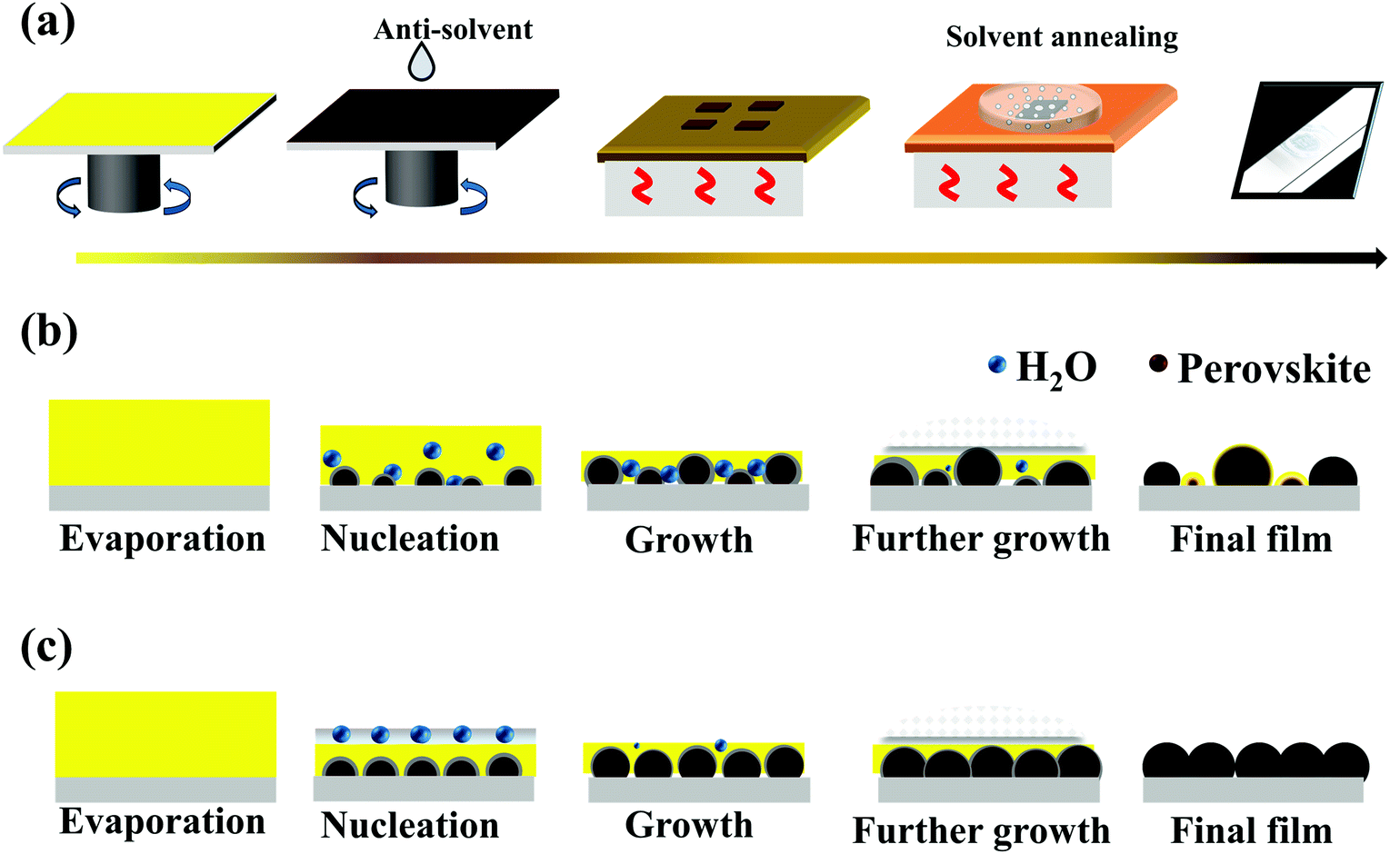 | ||
| Fig. 1 (a) Schematic illustration of the anti-solvent assisted crystallization process for fabricating perovskite films. (b) Model of the nucleation/growth competition of the perovskite crystal grown from the precursor solution using ordinary anti-solvents in ambient air. (c) Model of the nucleation/growth competition of the perovskite crystal grown from the precursor solution using the TBA anti-solvent in ambient air. | ||
Based on the physical properties of TBA, SBA and IBA mentioned in Table 1, we found that TBA has the relatively highest vapor pressure (46.0 ± 0.3 mmHg), lowest boiling point (84.6 ± 8.0 °C), lowest polarity (0.389), and optimal water solubility. These properties favor TBA anti-solvent assisted perovskite nucleation in the air for the following reasons: (1) the high vapor pressure and low boiling point greatly accelerate the evaporation of excess DMF; (2) the low polarity facilitates rapid nucleation and formation of the adduct MAI·PbI2·DMSO; (3) the high water solubility reduces the impact of moisture in the intermediate phase during the spin coating process. Moreover, TBA is an eco-friendly solvent with low toxicity and almost harmless to the human body and environment. Thus, it is reasonable to believe that TBA is an ideal anti-solvent for the preparation of a high-quality perovskite film in ambient air.
| Solvent | 3D structure | Vapor pressure at 25 °C (mmHg) | Boiling point (°C) | Polarity | Solubility in H2O (g/100 mL) |
|---|---|---|---|---|---|
| TBA |

|
46.0 ± 0.3 | 84.6 ± 8.0 | 0.389 | Soluble |
| SBA |

|
25.2 ± 0.3 | 96.6 ± 3.0 | 0.506 | 12.5 |
| IBA |

|
16.4 ± 0.4 | 105.0 ± 8.0 | 0.552 | 9.5 |
The nucleation effect of the MAI·PbI2·DMSO intermediate phase with different butanol-based anti-solvents was investigated by Fourier transform infrared (FTIR) spectroscopy. Fig. 2a shows FTIR spectra of the unannealed MAPbI3 films prepared using different anti-solvents (TBA, SBA, and IBA), which diaplayed similar absorbance peak positions. All the unannealed films exhibited N–H vibration peaks at approximately 3200 cm−1 (green line) and S![[double bond, length as m-dash]](https://www.rsc.org/images/entities/char_e001.gif) O stretching at around 1020 cm−1 attributed to DMSO (red line).44 By comparing the ratio of absorbance at 1020 cm−1 to the absorbance at 3200 cm−1, the concentration of DMSO in the intermediate phase could be inferred indirectly. From the results of this ratio (Fig. 2b), it was found that the DMSO content increased sequentially from TBA-treated perovskite (TBA-PVK), through SBA-treated perovskite (SBA-PVK) to IBA treated perovskite (IBA-PVK). The low ratio indicated few intermediate phases of MAI·PbI2·DMSO, which means the speed-up of the perovskite formation process.45 Typically, the intermediate phase of MAI·PbI2·DMSO is detrimental because of the slow release of DMSO from the spin-coated intermediate film, which results in a poor-quality MAPbI3 film.46 Moreover, Fig. S2a (ESI†) and Fig. 2b show the morphology of the fresh perovskite film with and without annealing using different anti-solvents, respectively.47 The color of the unannealed films was found to gradually change from dark brown (TBA-PVK) to yellowish brown (IBA-PVK), which implies that the content of DMSO in mesophase films increased. The results are well consistent with the observations from the FTIR spectra. In addition, compared with the annealed films in Fig. S2b (ESI†), the characteristic peak of DMSO disappeared, which indicates that the intermediate state of perovskite had transformed in the crystal growth process. Moreover, when 1% vol of deionized water was added to the anti-solvents, the intermediate phase of the TBA-PVK remained nearly invariable, while those of the others with less water-solubility decreased obviously (Fig. S3c and d, ESI†), further demonstrating the advantage of more water-soluble anti-solvents in the ambient fabrication of perovskites.
O stretching at around 1020 cm−1 attributed to DMSO (red line).44 By comparing the ratio of absorbance at 1020 cm−1 to the absorbance at 3200 cm−1, the concentration of DMSO in the intermediate phase could be inferred indirectly. From the results of this ratio (Fig. 2b), it was found that the DMSO content increased sequentially from TBA-treated perovskite (TBA-PVK), through SBA-treated perovskite (SBA-PVK) to IBA treated perovskite (IBA-PVK). The low ratio indicated few intermediate phases of MAI·PbI2·DMSO, which means the speed-up of the perovskite formation process.45 Typically, the intermediate phase of MAI·PbI2·DMSO is detrimental because of the slow release of DMSO from the spin-coated intermediate film, which results in a poor-quality MAPbI3 film.46 Moreover, Fig. S2a (ESI†) and Fig. 2b show the morphology of the fresh perovskite film with and without annealing using different anti-solvents, respectively.47 The color of the unannealed films was found to gradually change from dark brown (TBA-PVK) to yellowish brown (IBA-PVK), which implies that the content of DMSO in mesophase films increased. The results are well consistent with the observations from the FTIR spectra. In addition, compared with the annealed films in Fig. S2b (ESI†), the characteristic peak of DMSO disappeared, which indicates that the intermediate state of perovskite had transformed in the crystal growth process. Moreover, when 1% vol of deionized water was added to the anti-solvents, the intermediate phase of the TBA-PVK remained nearly invariable, while those of the others with less water-solubility decreased obviously (Fig. S3c and d, ESI†), further demonstrating the advantage of more water-soluble anti-solvents in the ambient fabrication of perovskites.
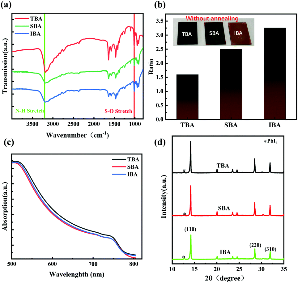 | ||
| Fig. 2 (a) FTIR spectra of the MAPbI3 perovskite prepared using TBA, SBA, and IBA without annealing. (b) The ratio of the absorbance intensity of the unannealed perovskite films at 1020 and 3200 cm−1 (1020 cm−1:3200 cm−1). The appearance of the unannealed perovskite films prepared with the anti-solvent (inset). (c) UV–vis absorption spectra of the MAPbI3 perovskite prepared using TBA, SBA, and IBA solvents with the annealing process. (d) XRD patterns of MAPbI3 films on ITO substrates prepared using different anti-solvents. | ||
The UV-visible absorption spectra (range from 500 nm to 800 nm) of the perovskite films prepared with different anti-solvents were measured, as shown in Fig. 2c. The absorption spectra of MAPbI3 films are similar with an absorption edge of ≈770 nm. Yet, it is also obvious that the absorption of TBA-PVK is slightly larger than those of the films fabricated using pure SBA and IBA anti-solvents. This illustrates that the TBA anti-solvent improved the optical absorption characteristics of the perovskite films.
To further elucidate the influence of different anti-solvents on the crystallization of the perovskite films, the X-ray diffraction (XRD) patterns of the three perovskite films deposited on the ITO substrate were investigated (Fig. 2d). The typical strong diffraction peaks located at 14.12°, 28.44° and 31.88° for the 2θ scan were observed, corresponding to the crystal planes of (110), (220) and (310), respectively, which were in good agreement with previous reports.25 The results confirmed that the films are highly crystallized perovskite phases. Simultaneously, a weak diffraction pattern of PbI2 appeared at 12.7° as shown in Fig. 2d. We speculate that the residual content of PbI2 could be related to the different solubilities of PbI2 and MAI compounds in various anti-solvents.48
To investigate the influence of the three butanol-based anti-solvents on the film morphology, top-view scanning electron microscopy (SEM) (Fig. 3a–c and j–l) and atomic force microscopy (AFM) measurements (Fig. 3g–i) were conducted on the prepared perovskite films. The TBA-PVK films exhibited an extremely homogeneous, smooth, pinhole-free polycrystalline morphology, which is shown in Fig. 3a and j. In particular, the average grain size of TBA-PVK was about 410.9 nm, which is significantly larger than those of the other films in Fig. 3d. The SBA-PVK films became slightly inhomogeneous (Fig. 3b and k), and it could be observed from Fig. 3e that the average grain size decreases to 310 nm. In particular, the grain size in the IBA-PVK films became smaller and the presence of disordered overlapping coverage was exceedingly prominent (Fig. 3c). This result is in agreement with the image in Fig. 3l, where parts of the film (indicated by yellow dotted lines) appeared luminous. The grain size of the perovskite gradually increased, which may be related to the DMSO content in the intermediate perovskite phase.49 Furthermore, the root mean square surface roughness values were measured to be 18.6, 21.5, and 23.9 nm for TBA-PVK, SBA-PVK, and IBA-PVK, respectively. TBA-PVK exhibited the relatively smoothest surface, which means fewer surface defect states and recombination. The 3D surface plot images (Fig. S3a, ESI†) also vividly confirm the variation of the surface roughness of perovskite films. In addition, to illustrate the effect of solvent annealing, the morphology characterization of perovskite films without solvent annealing has been added to Fig. S3b and c (ESI†).
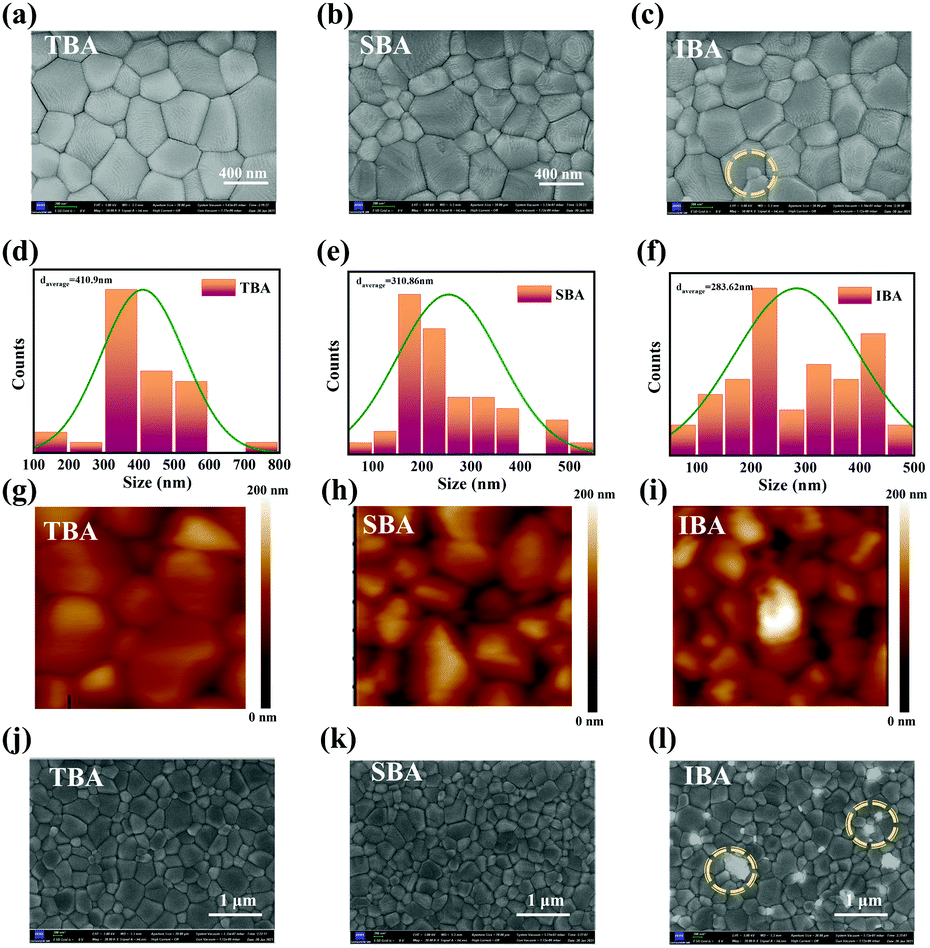 | ||
| Fig. 3 (a–c) Top-view SEM images of (a) TBA-PVK, (b) SBA-PVK, and (c) IBA-PVK films; the scale bar is 400 nm. (d–f) Grain-size distribution histograms of (d) TBA-PVK, (e) SBA-PVK, and (f) IBA-PVK films. (g–i) AFM images of (g) TBA-PVK, (h) SBA-PVK, and (i) IBA-PVK films. The scanning range of the images is 1 μm × 1 μm. (j–l) Top-view SEM images of (j) TBA-PVK, (k) SBA-PVK, and (l) IBA-PVK films; the scale bar is 1 μm. | ||
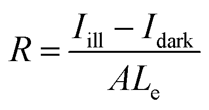
The optoelectronic properties of the PPDs fabricated using different anti-solvents were measured under dark conditions and the illumination of a 532 nm laser. Fig. 4a shows the current variation of PDs processed using different anti-solvents with the change in applied bias voltage under the illumination of 1 mW cm−2. The dark current of TBA-treated perovskite PDs (TBA-PPDs) was significantly lower than those of the SBA-treated perovskite PDs (SBA-PPDs) and IBA-treated perovskite PDs (IBA-PPDs) under negative bias. The photocurrent of TBA-PPD was also one order of magnitude higher than those of the other PDs under illumination, indicating that TBA is indeed a suitable anti-solvent that can markedly enhance the performance of PPDs. Specifically, the above results can be attributed to the fact the TBA-PVK film has better crystallization and morphological characteristics than the other films, which can effectually suppress the recombination loss caused by grain boundaries and intrinsic defects, thereby resulting in a lower dark current and a higher photocurrent. We further studied the dependence of the photocurrent on the light intensity of TBA-PPD. Fig. 4b displays the I–V curves under illumination using a 532 nm laser with different power densities. The results show that the photocurrent increased remarkably with the increase in power density. Particularly when the power density is 1000 μW cm−2, the photocurrent increases by nearly two orders of magnitude compared with the dark state, demonstrating that TBA-PPD has a satisfactory photocurrent response. To evaluate the advancement in the TBA-PPD, the responsivity (R) is also calculated according to the equation:50
 | (1) |
 | (2) |
 | (3) |
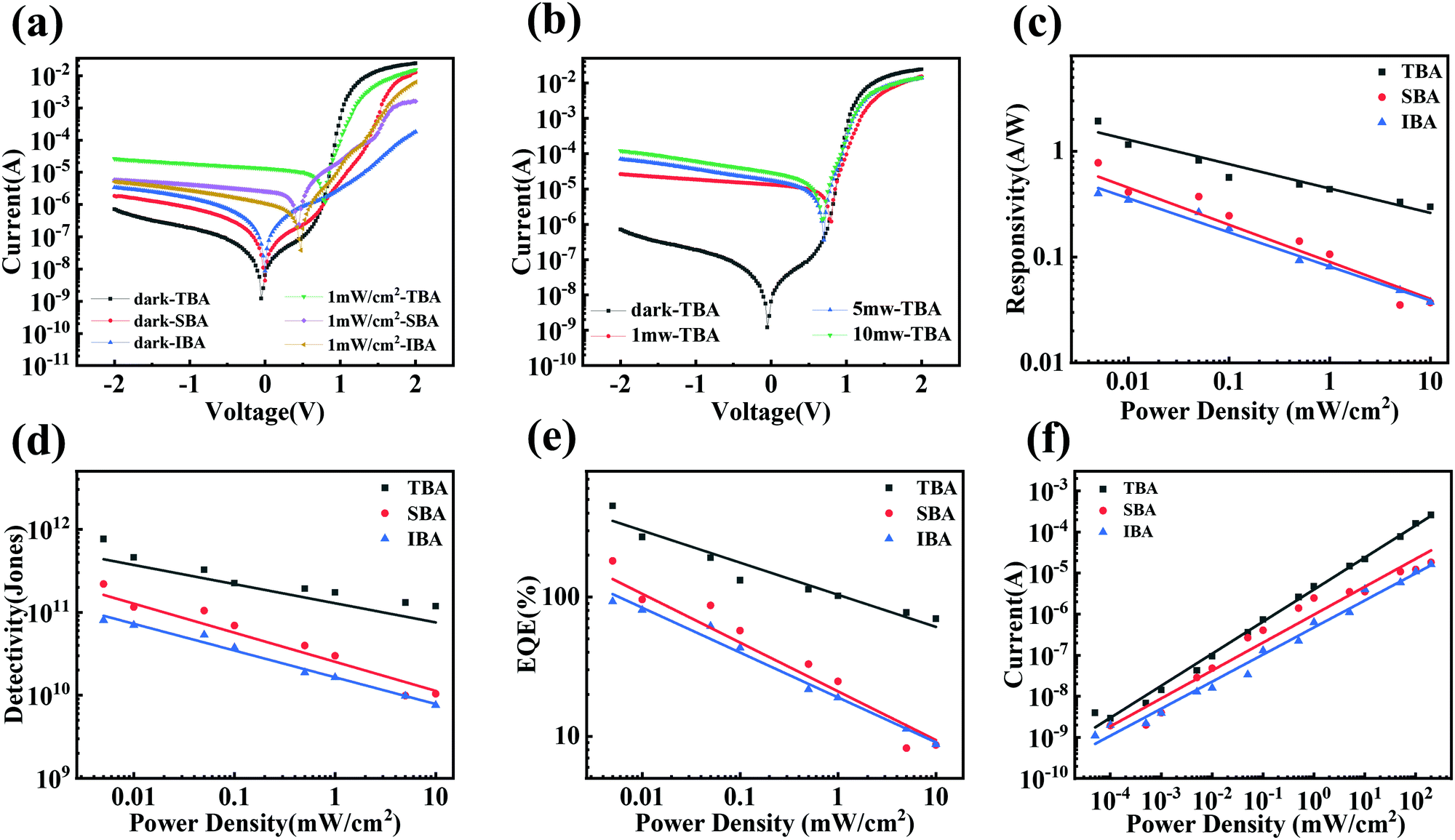 | ||
| Fig. 4 Electrical properties of PDs. (a) I–V characteristics of PDs treated using different anti-solvents under dark conditions and monochromatic illumination at a wavelength of 532 nm with a power density of 1 mW cm−2. (b) I–V characteristics of TBA-PD under dark conditions and monochromatic illumination at a wavelength of 532 nm with different power densities. Dependences of (c) responsivity, (d) detectivity, and (e) EQE of PDs treated using different anti-solvents on the power densities under monochromatic illumination at a wavelength of 532 nm with a bias of −2 V. (f) LDR curves of PDs treated using different anti-solvents under monochromatic illumination at a wavelength of 532 nm with a bias of 0 V. | ||
| Device structure | Wavelength (nm) | Responsivity (A W−1) | Detectivity (Jones) | Processing condition | Ref. |
|---|---|---|---|---|---|
| ITO/PEDOT:PSS/MAPbI3/PCBM/BCP/Al | 500 | 0.87 | 9.1 × 10¹¹ | Inert gas protection | 54 |
| ITO/TiO2/PCBM/MAPbI3/P3HT/MoO3/Ag | 500 | 0.34 | 4.8 × 10¹² | Inert gas protection | 55 |
| ITO/PEDOT:PSS/MAPbI3/PCBM/Al | 670 | 0.314 | — | Inert gas protection | 56 |
| ITO/PEDOT:PSS/MAPbI3/PCBM/AZO/Al | 700 | 0.3 | — | Inert gas protection | 57 |
| ITO/PEDOT:PSS/MAPbI3/PCBM/BCP/Ag | 532 | 1.06 | 1.48 × 10¹¹ | Inert gas protection | 58 |
| FTO/TiO2/MAPbI3/Spiro/Au | 660 | 0.18 | 6.3 × 10¹⁰ | Inert gas protection | 59 |
| FTO/TiO2/Al2O3/PCBM/MAPbI3/Spiro/Au/Ag | 600 | 0.4 | ∼1012 | Inert gas protection | 60 |
| ITO/NiOx/MAPbI3/PMMA/C70/BCP/Cu | 400–800 | 0.1–0.5 | ∼1011 | Inert gas protection | 61 |
| ITO/PEDOT:PSS/MAPbI3/PCBM/BCP/Ag (TBA-PDs) | 532 | 1.93 | 7.62 × 10¹¹ | Air conditions | This work |
| ITO/PEDOT:PSS/MAPbI3/PCBM/BCP/Ag (SBA-PDs) | 532 | 0.78 | 2.19 × 10¹¹ | Air conditions | This work |
| ITO/PEDOT:PSS/MAPbI3/PCBM/BCP/Ag (IBA-PDs) | 532 | 0.40 | 8.03 × 10¹⁰ | Air conditions | This work |
The linear weak-light response range is customarily characterized by the linear dynamic range (LDR), defined by the following equation:53
 | (4) |
mW cm−2 with a 532nm laser. This result corresponds to a LDR value of 104 dB for the TBA-PPD. This linear response might have resulted from the excellent carrier transport properties of TBA-PVK and the low electron trap density in the whole photodetector. The LDR values of SBA-PPD and IBA-PPD are 72 dB and 71 dB, respectively.
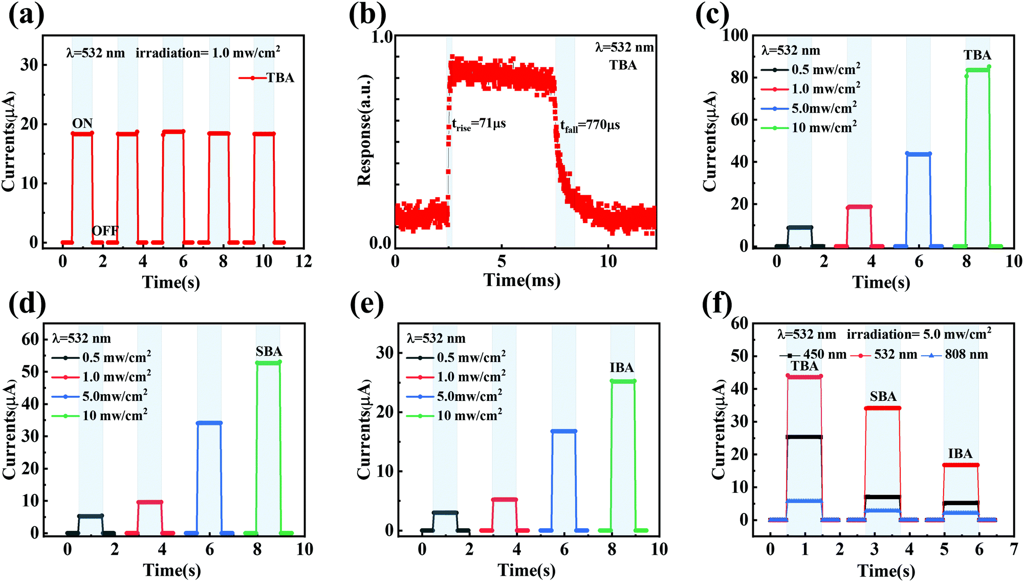
To explore the instantaneous photoresponse time characteristics, the current–time (I–T) curves were measured at a 0 V bias under 532 nm laser irradiation with a light density of 1 mW cm−2 for TBA-PPDs, as shown in Fig. 5a. The device displays striking on–off stability and cycle repeatability, revealing the application potential of TBA-PPD in optical modulation switches. Besides, the corresponding photocurrent responses of SBA-PPD and IBA-PPD are shown in Fig. S5 and S6 (ESI†). To accurately evaluate the response times of the devices, we measured the response times of different PPDs under irradiation using a 532 nm pulse laser with a modulation frequency of 100 Hz. As illustrated in Fig. 5b, the rise time (trise) and fall time (tfall) of TBA-PPD are 71 μs and 770 μs, respectively. The rise and fall times of SBA-PPD are 135 μs and 2.56 ms (Fig. S5a, ESI†), while the corresponding ones for IBA-PPD are 1.29 ms and 3.58 ms, respectively (Fig. S6a, ESI†).
 | ||
| Fig. 5 (a) Photoswitching characteristics of the TBA-PPD under 532 nm light illumination as the light circulates on and off (1 mW cm−2, VBias = 0 V). (b) Response time measurement under one on–off illumination cycle of a 532 nm laser with a pulse frequency of 100 Hz. (c–e) Photocurrent responses of TBA-PPD, SBA-PPD and IBA-PPD under 532 nm light illumination at different power densities, respectively. (f) Photocurrent response of PDs processed using different anti-solvents under 532, 450, and 808 nm light illumination with a power density of 5 mW cm−2. | ||
The instantaneous photocurrent measured under 532 nm laser irradiation increases significantly with the increase of power density in the range of 0.5 to 10 mW cm−2 (Fig. 5c). It can be seen from Fig. 4f and 5c that the photocurrent increases visibly with the increase in irradiation power, and the trend of both side curves is in agreement. The TBA-PPD can achieve an effective optical switch response under different power densities ranging from 100 nW cm−2 to 190 mW cm−2. A similar growth trend of instantaneous photocurrent could also be observed with the 450 nm laser (Fig. S4a, ESI†) and 808 nm laser (Fig. S4b, ESI†) illuminations with different power densities, reflecting the excellent optical switch response characteristics of TBA-PPD, which is of great significance for its practical applications. The photocurrent responses of SBA-PPD and IBA-PPD under 450 and 808 nm laser illuminations at different power densities are presented in Fig. S5b, c and S6b, c (ESI†), respectively.
For further observation, we tested the photocurrents of the above three anti-solvent-treated PDs under 450, 532, and 808 nm laser illuminations with a specific incident power density of 1 mW cm−2 and a bias voltage of 0 V. Fig. 5f shows the light current response characteristics of three PPDs under laser illumination at different wavelengths. Interestingly, all PPDs displayed the weakest response intensity to the 808 nm laser and the most marked response intensity to the 532 nm laser, showing no difference from the absorption spectra, as plotted in Fig. 2c. Notably, regardless of the illumination wavelength, TBA-PPD showed the best photocurrent response. This also proves that TBA is more likely to avoid the influence of humidity in the air, facilitating nucleation and grain growth than SBA and IBA, to obtain perovskite films with good crystallinity and improved device performance. Furthermore, as depicted in Fig. S4c (ESI†), the histogram corresponding to the photocurrent response at the three illumination wavelengths more intuitively confirms this conclusion.
Conclusions
In summary, we have demonstrated an effective anti-solvent-assisted nucleation management strategy for the ambient preparation of high-performance PPDs. We disclosed a key finding that, compared with SBA and IBA anti-solvents, the eco-friendly TBA could effectively reduce the influence of airborne moisture and improve the nucleation process, ultimately producing high-quality perovskite films with uniform, smooth, pinhole-free surface morphology. This TBA-optimized perovskite photodetector showed a high responsivity of 1.93 A W−1 under the illumination of a 532 nm laser with a power density of 5 μW cm−2 at a bias voltage of −2 V, a high detectivity of 7.62 × 10¹¹ Jones, and a large LDR of 104 dB. To the best of our knowledge, the responsivity performance of this photodetector is the highest among the same vertical device structures and even markedly exceeds some of the reported devices prepared in an inert atmosphere. Hence, it is believed that this study can provide an ideal green route for the fabrication of high-performance PPDs in ambient air and may pave the way for massive and low-cost manufacturing of PPDs.Conflicts of interest
There are no conflicts to declare.Acknowledgements
This work was supported by the National Natural Science Foundation of China (No. 61675147, 61735010, and 91838301), the National Key Research and Development Program of China (No. 2017YFA0700202), the Basic Research Program of Shenzhen (JCYJ20170412154447469), Beiyang Yong Junior Faculties of Tianjin University (No. 2019XRG-0056), the Innovation Projects of the Department of Education of Guangdong Province (2018KQNCX264) and Wenzhou City Governmental Public Industrial Technology Project (G20160014).References
- Y. J. Fang, Q. F. Dong, Y. C. Shao, Y. B. Yuan and J. S. Huang, Nat. Photonics, 2015, 9, 679–687 CrossRef CAS.
- F. P. García de Arquer, A. Armin, P. Meredith and E. H. Sargent, Nat. Rev. Mater., 2017, 2, 16100 CrossRef.
- C. Bao, J. Yang, S. Bai, W. Xu, Z. Yan, Q. Xu, J. Liu, W. Zhang and F. Gao, Adv. Mater., 2018, 30, e1803422 CrossRef PubMed.
- C. Li, J. Lu, Y. Zhao, L. Sun, G. Wang, Y. Ma, S. Zhang, J. Zhou, L. Shen and W. Huang, Small, 2019, 15, e1903599 CrossRef PubMed.
- J. Wang, S. Xiao, W. Qian, K. Zhang, J. Yu, X. W. Xu, G. P. Wang, S. Z. Zheng and S. H. Yang, Adv. Mater., 2021, 33, 9 Search PubMed.
- X. D. Qiu, X. G. Yu, S. Yuan, Y. H. Gao, X. M. Liu, Y. Xu and D. R. Yang, Adv. Opt. Mater., 2018, 6, 1700638 CrossRef.
- I. Vurgaftman, J. R. Meyer and L. R. Ram-Mohan, J. Appl. Phys., 2001, 89, 5815–5875 CrossRef CAS.
- R. R. Zhuo, L. H. Zeng, H. Y. Yuan, D. Wu, Y. G. Wang, Z. F. Shi, T. T. Xu, Y. T. Tian, X. J. Li and Y. H. Tsang, Nano Res., 2019, 12, 183–189 CrossRef CAS.
- H. Cho, S. H. Jeong, M. H. Park, Y. H. Kim, C. Wolf, C. L. Lee, J. H. Heo, A. Sadhanala, N. Myoung, S. Yoo, S. H. Im, R. H. Friend and T. W. Lee, Science, 2015, 350, 1222–1225 CrossRef CAS PubMed.
- Y. Li, Z. F. Shi, S. Li, L. Z. Lei, H. F. Ji, D. Wu, T. T. Xu, Y. T. Tian and X. J. Li, J. Mater. Chem. C, 2017, 5, 8355–8360 RSC.
- Y. Fang and J. Huang, Adv. Mater., 2015, 27, 2804–2810 CrossRef CAS PubMed.
- Q. Jiang, Y. Zhao, X. Zhang, X. Yang, Y. Chen, Z. Chu, Q. Ye, X. Li, Z. Yin and J. You, Nat. Photonics, 2019, 13, 460–466 CrossRef CAS.
- Y. Li, Z. F. Shi, W. Q. Liang, L. T. Wang, S. Li, F. Zhang, Z. Z. Ma, Y. Wang, Y. Z. Tian, D. Wu, X. J. Li, Y. T. Zhang, C. X. Shan and X. S. Fang, Mater. Horiz., 2020, 7, 530–540 RSC.
- Y. Li, Z. F. Shi, L. T. Wang, Y. C. Chen, W. Q. Liang, D. Wu, X. J. Li, Y. Zhang, C. X. Shan and X. S. Fang, Mater. Horiz., 2020, 7, 1613–1622 RSC.
- M. Ahmadi, T. Wu and B. Hu, Adv. Mater., 2017, 29, 1605242 CrossRef PubMed.
- L. Dou, Y. M. Yang, J. You, Z. Hong, W. H. Chang, G. Li and Y. Yang, Nat. Commun., 2014, 5, 5404 CrossRef CAS PubMed.
- W. Hu, R. S. Wu, S. Z. Yang, P. Fan, J. L. Yang and A. L. Pan, J. Phys. D: Appl. Phys., 2017, 50, 375101 CrossRef.
- A. K. Jena, A. Kulkarni and T. Miyasaka, Chem. Rev., 2019, 119, 3036–3103 CrossRef CAS PubMed.
- L. Shen, Y. Fang, D. Wang, Y. Bai, Y. Deng, M. Wang, Y. Lu and J. Huang, Adv. Mater., 2016, 28, 10794–10800 CrossRef CAS PubMed.
- X. Hu, X. D. Zhang, L. Liang, J. Bao, S. Li, W. L. Yang and Y. Xie, Adv. Funct. Mater., 2014, 24, 7373–7380 CrossRef CAS.
- J. A. Christians, P. A. Miranda Herrera and P. V. Kamat, J. Am. Chem. Soc., 2015, 137, 1530–1538 CrossRef CAS PubMed.
- Y. Zhang, A. Kirs, F. Ambroz, C. T. Lin, A. S. R. Bati, I. P. Parkin, J. G. Shapter, M. Batmunkh and T. J. Macdonald, Small Methods, 2020, 5, 2000744 CrossRef.
- T. L. Bu, L. Wu, X. P. Liu, X. K. Yang, P. Zhou, X. X. Yu, T. S. Qin, J. J. Shi, S. Wang, S. S. Li, Z. L. Ku, Y. Peng, F. Z. Huang, Q. B. Meng, Y. B. Cheng and J. Zhong, Adv. Energy Mater., 2017, 7, 1700576 CrossRef.
- H. Li, Y. Xia, C. Wang, G. Wang, Y. Chen, L. Guo, D. Luo and S. Wen, ACS Appl. Mater. Interfaces, 2019, 11, 34989–34996 CrossRef CAS PubMed.
- Y. Yu, S. Yang, L. Lei, Q. Cao, J. Shao, S. Zhang and Y. Liu, ACS Appl. Mater. Interfaces, 2017, 9, 3667–3676 CrossRef CAS PubMed.
- Y. Yun, F. Wang, H. Huang, Y. Fang, S. Liu, W. Huang, Z. Cheng, Y. Liu, Y. Cao, M. Gao, L. Zhu, L. Wang, T. Qin and W. Huang, Adv. Mater., 2020, 32, e1907123 CrossRef PubMed.
- J. J. Duan, Z. Y. Liu, Y. F. Zhang, K. K. Liu, T. W. He, F. Wang, J. Dai and P. X. Zhou, Opt. Mater., 2018, 85, 55–60 CrossRef CAS.
- H. S. Ko, J. W. Lee and N. G. Park, J. Mater. Chem. A, 2015, 3, 8808–8815 RSC.
- L. Shi, H. Hao, J. Dong, T. Zhong, C. Zhang, J. Hao, J. Xing and H. Liu, Nanomaterials, 2019, 9, 915 CrossRef CAS PubMed.
- R. Singh, S. Sandhu, H. Yadav and J. J. Lee, ACS Appl. Mater. Interfaces, 2019, 11, 29941–29949 CrossRef CAS PubMed.
- J. Z. Song, J. H. Li, X. M. Li, L. M. Xu, Y. H. Dong and H. B. Zeng, Adv. Mater., 2015, 27, 7162–7167 CrossRef CAS PubMed.
- Y. Yang, T. Chen, D. Q. Pan, J. Gao, C. T. Zhu, F. Y. Lin, C. H. Zhou, Q. D. Tai, S. Xiao, Y. B. Yuan, Q. L. Dai, Y. B. Han, H. P. Xie and X. Y. Guo, Nano Energy, 2020, 67, 104246 CrossRef CAS.
- X. M. Li, Y. Wu, S. L. Zhang, B. Cai, Y. Gu, J. Z. Song and H. B. Zeng, Adv. Funct. Mater., 2016, 26, 2435–2445 CrossRef CAS.
- J. W. Chen, J. Wang, X. B. Xu, J. H. Li, J. Z. Song, S. Lan, S. N. Liu, B. Cai, B. N. Han, J. T. Precht, D. Ginger and H. B. Zeng, Nat. Photonics, 2021, 15, 9 Search PubMed.
- C. Hu, S. B. Shivarudraiah, H. H. Y. Sung, I. D. Williams, J. E. Halpert and S. H. Yang, Sol. RRL, 2021, 2000712, DOI:10.1002/solr.202000712.
- M. Xiao, L. Zhao, M. Geng, Y. Li, B. Dong, Z. Xu, L. Wan, W. Li and S. Wang, Nanoscale, 2018, 10, 12141–12148 RSC.
- J. W. Jung, S. T. Williams and A. K. Y. Jen, RSC Adv., 2014, 4, 62971–62977 RSC.
- M. Yavari, M. Mazloum-Ardakani, S. Gholipour, M. M. Tavakoli, S. H. Turren-Cruz, N. Taghavinia, M. Gratzel, A. Hagfeldt and M. Saliba, Adv. Energy Mater., 2018, 8, 1800177 CrossRef.
- P. Luo, W. Xia, S. Zhou, L. Sun, J. Cheng, C. Xu and Y. Lu, J. Phys. Chem. Lett., 2016, 7, 3603–3608 CrossRef CAS PubMed.
- F. Yang, G. Kapil, P. Zhang, Z. Hu, M. A. Kamarudin, T. Ma and S. Hayase, ACS Appl. Mater. Interfaces, 2018, 10, 16482–16489 CrossRef CAS PubMed.
- C. Capello, U. Fischer and K. Hungerbuhler, Green Chem., 2007, 9, 927–934 RSC.
- D. Prat, J. Hayler and A. Wells, Green Chem., 2014, 16, 4546–4551 RSC.
- S. Ghosh, S. Mishra and T. Singh, Adv. Mater. Interfaces, 2020, 7, 2000950 CrossRef CAS.
- N. J. Jeon, J. H. Noh, Y. C. Kim, W. S. Yang, S. Ryu and S. I. Seok, Nat. Mater., 2014, 13, 897–903 CrossRef CAS PubMed.
- M. S. Yin, F. X. Xie, H. Chen, X. D. Yang, F. Ye, E. B. Bi, Y. Z. Wu, M. T. Cai and L. Y. Han, J. Mater. Chem. A, 2016, 4, 8548–8553 RSC.
- N. Ahn, D.-Y. Son, I.-H. Jang, S. M. Kang, M. Choi and N.-G. Park, J. Am. Chem. Soc., 2015, 137, 8696–8699 CrossRef CAS PubMed.
- Y. Bai, S. Xiao, C. Hu, T. Zhang, X. Y. Meng, Q. Li, Y. L. Yang, K. S. Wong, H. N. Chen and S. H. Yang, Nano Energy, 2017, 34, 58–68 CrossRef CAS.
- Y. F. Wang, J. Wu, P. Zhang, D. T. Liu, T. Zhang, L. Ji, X. L. Gu, Z. D. Chen and S. B. Li, Nano Energy, 2017, 39, 616–625 CrossRef CAS.
- M. Konstantakou, D. Perganti, P. Falaras and T. Stergiopoulos, Crystals, 2017, 7, 291 CrossRef.
- F. Li, C. Ma, H. Wang, W. Hu, W. Yu, A. D. Sheikh and T. Wu, Nat. Commun., 2015, 6, 8238 CrossRef PubMed.
- F. G. Yan, Z. M. Wei, X. Wei, Q. S. Lv, W. K. Zhu and K. Y. Wang, Small Methods, 2018, 2, 1700349 CrossRef.
- Z.-Y. Peng, J.-L. Xu, J.-Y. Zhang, X. Gao and S.-D. Wang, Adv. Mater. Interfaces, 2018, 5, 1870089 CrossRef.
- H. Wang and D. H. Kim, Chem. Soc. Rev., 2017, 46, 5204–5236 RSC.
- C. Liu, H. Peng, K. Wang, C. D. Wei, Z. X. Wang and X. Gong, Nano Energy, 2016, 30, 27–35 CrossRef CAS.
- C. Liu, K. Wang, C. Yi, X. Shi, P. Du, A. W. Smith, A. Karim and X. Gong, J. Mater. Chem. C, 2015, 3, 6600–6606 RSC.
- C. Bao, W. Zhu, J. Yang, F. Li, S. Gu, Y. Wang, T. Yu, J. Zhu, Y. Zhou and Z. Zou, ACS Appl. Mater. Interfaces, 2016, 8, 23868–23875 CrossRef CAS PubMed.
- X. Zhang, C. C. Liu, G. Ren, S. Y. Li, C. H. Bi, Q. Y. Hao and H. Liu, Nanomaterials, 2018, 8, 318 CrossRef PubMed.
- T. T. Li, Q. Y. Li, X. Tang, Z. L. Chen, Y. F. Li, H. L. Zhao, S. L. Wang, X. Ding, Y. T. Zhang and J. Q. Yao, J. Phys. Chem. C, 2021, 125, 2850–2859 CrossRef CAS.
- H. Tao, H. Wang, Y. Bai, H. Zhao, Q. Fu, Z. Ma and H. Long, J. Mater. Chem. C, 2020, 8, 6228–6235 RSC.
- B. R. Sutherland, A. K. Johnston, A. H. Ip, J. Xu, V. Adinolfi, P. Kanjanaboos and E. H. Sargent, ACS Photonics, 2015, 2, 1117–1123 CrossRef CAS.
- J. Peng, L. Cui, R. Li, Y. Xu, L. Jiang, Y. Li, W. Li, X. Tian and Q. Lin, J. Mater. Chem. C, 2019, 7, 1859–1863 RSC.
Footnotes |
| † Electronic supplementary information (ESI) available. See DOI: 10.1039/d1tc01726h |
| ‡ These authors contributed equally to this work. |
| This journal is © The Royal Society of Chemistry 2021 |