
 Open Access Article
 This Open Access Article is licensed under a Creative Commons Attribution-Non Commercial 3.0 Unported Licence
Exploring swift-heavy ion irradiation of InGaN/GaN multiple quantum wells for green-emitters: the use of Raman and photoluminescence to assess the irradiation effects on the optical and structural properties†
José
Cardoso
 *a,
Nabiha
Ben Sedrine
a,
Przemysław
Jóźwik
b,
Miguel C.
Sequeira
b,
Christian M.
Wetzel
c,
Clara
Grygiel
d,
Katharina
Lorenz
be,
Teresa
Monteiro
a and
Maria Rosário P.
Correia
*a
*a,
Nabiha
Ben Sedrine
a,
Przemysław
Jóźwik
b,
Miguel C.
Sequeira
b,
Christian M.
Wetzel
c,
Clara
Grygiel
d,
Katharina
Lorenz
be,
Teresa
Monteiro
a and
Maria Rosário P.
Correia
*a
aDepartamento de Física & i3N, Universidade de Aveiro, Campus Universitário de Santiago, 3810-193 Aveiro, Portugal. E-mail: jose.cardoso@ua.pt
bIPFN, Instituto Superior Técnico, Campus Tecnológico e Nuclear, Estrada Nacional 10, P 2695-066 Bobadela LRS, Portugal
cDepartment of Materials Science and Engineering and Department of Physics, Applied Physics and Astronomy, Rensselaer Polytechnic Institute, Troy, NY 12180, USA
dCIMAP, CEA-CNRS-ENSICAEN-UNICAEN, 14070 Caen Cedex 5, France
eInstituto de Engenharia de Sistemas de Computadores – Microsistemas e Nanotecnologia (INESC-MN), Rua Alves Redol, 1000-029 Lisboa, Portugal
First published on 9th July 2021
Abstract
The effects of 129Xe swift-heavy ion (SHI) irradiation on the optical and structural properties of InGaN/GaN multiple quantum wells (MQWs) are studied using non-destructive optical spectroscopy techniques. Through excitation wavelength-dependent μ-Raman spectroscopy, it is possible to identify the damage profile and to notice the surface region (around the first 40 nm) as the most affected one. Independent Rutherford backscattering spectrometry in channelling mode experiments corroborate this. By using resonant excitation with InGaN electronic states, it is possible to observe an increase of the A1(LO)InGaN phonon intensity for higher SHI energies. This is attributed to intermixing at the MQWs’ interfaces for electronic energy losses above 20 keV nm−1. Photoluminescence studies reveal an intense yellow emission band (YB) with two distinct contributions: excitonic (InGaN) and deep-level defects (GaN). After irradiation, strong luminescence intensity quenching and a change in its excitation mechanisms occur. The YB is no longer excited with energy above the GaN bandgap, but instead through an excitation band (at about 2.75 eV) attributed to gallium vacancies introduced in the GaN barriers. The strong quenching of the luminescence reveals that SHI irradiation introduces detrimental defects in the structure, which may compromise its use (without additional post-implantation treatments) for obtaining more efficient green light emitters based on InGaN/GaN MQWs.
1. Introduction
Group III–nitride (III–N) semiconductors have been widely exploited for optoelectronic applications with high-efficiency blue light-emitting diodes (LEDs) based on InGaN/GaN multiple quantum well (MQW) structures well established on the market.1,2 Tuning the emission to higher wavelengths by increasing the concentration of indium (In) leads to a decrease of the efficiency mainly due to spontaneous and piezoelectric polarization fields in the active region, and consequently in a strong quantum-confined Stark effect (QCSE).3,4 This becomes particularly problematic for green light emitters for which AlGaInP based solutions are also not efficient (the “green gap” problem).5The existence of an In compositional gradient in InGaN/GaN MQWs has been suggested to improve their emission efficiency by changing the electronic band structure in a way that reduces both QCSE and Auger losses.4,6,7 The control of these gradients at the nanoscale, during growth, is a tremendous challenge and, to accomplish this, post-growth treatments are suggested. Thermal annealing and/or low-energy ion irradiation have been applied to generate a mixture of group III atoms at quantum-well interfaces.8 This process is known as quantum well intermixing (QWI). In the first case, the samples are subjected to high temperature (1300–1400 °C) heat treatments, required for atomic interdiffusion, and to high-pressures (up to 15 kbar) to avoid surface decomposition.9,10 In the second case, low energy ion irradiation (tens to hundreds of keV) promotes QWI due to atomic displacements caused by elastic collisions between the energetic ions and the target nuclei. However, this gives rise to the creation of point defects, introducing nonradiative recombination mechanisms, which can further reduce the emission efficiency. Furthermore, because of the low penetration depth of these ions, their concentration is high in the active region, affecting both the electrical and optical properties of the material. To recover the damaged crystalline structure, post-irradiation thermal annealing is mandatory. This thermal treatment also promotes intermixing since irradiation breaks III–N bonds, facilitating interdiffusion at the interfaces during annealing.8,11
Swift-heavy ion (SHI) irradiation has emerged as a possible tool for materials engineering, such as intermixing in semiconducting multilayer structures.12–15 SHIs consist of energetic ions (with energies higher than 1 MeV per nucleon), for which the ion matter interaction is mainly governed by electronic excitations with the contribution of ballistic nuclear collisions being low.16 Due to intense local ionization, solid–liquid–solid transitions are induced in the material for a few tens to hundreds of picoseconds, promoting the formation of long and straight cylindrical ion tracks along the ion path. Atomic diffusion during the molten state along the track direction is a possibility in this energetic regime.17 SHI irradiation can also generate surface defects (e.g., sputtering and formation of voids within the first nanometers of the track), recover pre-damaged crystals, or even cause amorphization of the crystal.17,18 To induce the creation of ion tracks and intermixing at interfaces, the electronic energy loss should be higher than a specific threshold (Seth) that depends on the material properties (e.g., density and specific heat capacity). For GaN, the track formation threshold value is still under debate, with some contradictory values reported: (i) ∼15 keV nm−1,18 (ii) ∼17 keV nm−1,19 and (iii) higher than 22.8 keV nm−1.20 In addition to the possibility of QWI with an expected low density of point defects, the higher penetration depth of SHIs allows their implantation in the substrate instead of in the active region.
Studies about the impacts of SHI irradiation of InGaN/GaN MQWs are scarce and, to the best of our knowledge, only two reports involving irradiation with 40 MeV iodine ions, and 100 MeV gold ions can be found.21,22 In both studies, the luminescence intensity was found to be quenched after irradiation, and K. Prabakaran et al.22 suggest that QWI was achieved.
In this work, optical spectroscopic techniques, such as optical transmittance, μ-Raman (non-resonant and resonant), photoluminescence (PL), and PL excitation (PLE), were used to investigate the effects of xenon (129Xe) SHI irradiation on the optical and structural properties of InGaN/GaN MQWs and, thus, evaluate the possibility of using this approach for obtaining intermixing. Aluminium (Al) foils with different thicknesses were placed in front of the ion beam to perform a study varying the beam energy from 82 to 38 MeV, which corresponds to electronic (Se) and nuclear (Sn) energy losses at the surface changing from 21.5 to 13.0 keV nm−1 and from 0.23 to 0.42 keV nm−1, respectively. To validate the methodology adopted and analysis of the results carried out in this work, independent Rutherford backscattering spectrometry in channelling mode (RBS/C) experiments were conducted.
2. Experimental section
The InGaN/GaN MQWs were grown by metalorganic vapour phase epitaxy (MOVPE). Their structure consists of a five-period MQW structure: InGaN wells (∼2.7 nm) and GaN barriers (∼11 nm). The structure is grown on top of the GaN template layer (∼3 μm) on a (0001) sapphire substrate and capped by an 11 nm thick GaN layer (Fig. 1a).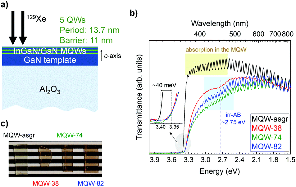 | ||
| Fig. 1 (a) Schematic representation of the InGaN/GaN MQW structure. (b) Optical transmittance spectra of the samples before and after irradiation with Xe SHI. The inset shows an enlargement around the GaN absorption edge. (c) Photo of the InGaN/GaN MQW samples showing the loss of transparency after irradiation. | ||
SHI irradiation was carried out at the Grand Accélérateur National d’Ions Lourds (GANIL) facilities using 92 MeV 129Xe ions with a fluence of 2 × 1012 cm−2 at room temperature (RT). The irradiation was done in a quasi-normal incidence configuration. Aluminium (Al) foils with different thicknesses were placed in front of the ion beam to perform a study varying the energy from 82 to 38 MeV. Monte Carlo simulations, obtained using the SRIM 2013 code,23 predict an implantation depth higher than 5 μm, implying that ions lose their energy predominantly by electronic processes throughout the active region, while the end-of-range (increased nuclear losses) occurs deep inside the sapphire substrate. The electronic (Se) and nuclear (Sn) energy losses at the surface are expected to vary from 21.5 to 13.0 keV nm−1 and from 0.23 to 0.42 keV nm−1 when decreasing the beam energy from 82 to 38 MeV, respectively. According to the references, these Se values are above and below the track formation threshold in GaN.18,19Table 1 summarizes the irradiation conditions (energy as well as electronic and nuclear losses) and the samples’ labels.
| Sample | Energy [MeV] | S e [keV nm−1] | S n [keV nm−1] |
|---|---|---|---|
| MQW-asgr | — | — | — |
| MQW-38 | 38 | 13.0 | 0.42 |
| MQW-74 | 74 | 20.3 | 0.27 |
| MQW-82 | 82 | 21.5 | 0.23 |
The optical transmittance was studied at RT using a double-beam Shimadzu UV-2100 UV/vis spectrometer in transmission mode from 190 to 900 nm.
μ-Raman was realized at RT using a Horiba Jobin Yvon micro-Raman HR800 spectrometer equipped with a charge-coupled device (CCD) for detection. Three different excitation laser lines were used: 325 nm (3.8 eV) and 442 nm (2.8 eV) from a He–Cd laser and 632.8 nm (1.96 eV) from a He–Ne laser. The experiments were carried out in the backscattering geometry z(x,·)![[z with combining macron]](https://www.rsc.org/images/entities/i_char_007a_0304.gif) , in which z is chosen to be parallel to the c-axis of the crystal. A confocal microscope with a 40× objective (numerical aperture: 0.47) was used for the 325 nm laser line and a 50× objective (numerical aperture: 0.5) was used for the other excitation laser lines. The experimental error was about 2 cm−1.
, in which z is chosen to be parallel to the c-axis of the crystal. A confocal microscope with a 40× objective (numerical aperture: 0.47) was used for the 325 nm laser line and a 50× objective (numerical aperture: 0.5) was used for the other excitation laser lines. The experimental error was about 2 cm−1.
RBS/C was performed at RT on a Van de Graaff AN-2500 Type-A accelerator facility using a 2 MeV helium (4He) ion beam and a silicon PIN diode detector placed at 165° relative to the beam direction. Post-irradiation damage was evaluated by Monte Carlo (MC) simulations using the computational code McChasy.24,25
RT PL and PLE were carried out using a Fluorolog 3 Horiba Scientific modular system equipped with a 450 W Xe arc lamp coupled to a monochromator. The emission/excitation was controlled by the entrance and exit monochromators. Both PL and PLE spectra were acquired in the front face geometry. The presented spectra were corrected to the spectral response of the optical components, the photomultiplier tube (PMT) detector, and the Xe lamp.
3. Results and discussion
3.1. Optical transmittance
The optical transmittance spectra of the InGaN/GaN MQWs before and after irradiation are shown in Fig. 1b. For MQW-asgr (the samples’ labels can be found in Table 1), the spectrum reveals well-defined GaN near band edge (NBE) absorption at 3.4 eV and an absorption tail with an onset at about 2.7 eV (represented by the shaded yellow region in Fig. 1b) related to the InGaN band edge. The perceived interference fringe pattern is due to the coherent superposition of multiple reflections in the GaN-based film. After irradiation, the effective GaN band edge redshifts about 40 meV (estimated using a sigmoidal function) and becomes less steep (inset in Fig. 1b). The transparency in the visible range is reduced as well (Fig. 1c). Furthermore, an irradiation-induced absorption band (irr-AB) is detected at about 2.75 eV, overlapped with the interference fringes and InGaN absorption tail. These results suggest that Xe SHI irradiation generates defects in the samples, which introduce localized electronic states near the electronic bands of GaN as well as a mid-gap state responsible for the absorption at 2.75 eV that, at first sight, can be related to both GaN (barriers and/or template) and InGaN.The optical transmittance spectra of c-plane GaN layers grown on sapphire and irradiated identically to the InGaN/GaN MQWs (Fig. S1 in the ESI†) also reveal irr-AB at about 2.75 eV. This suggests that the mid-gap states are related to GaN and not InGaN. Besides, if related to defects in InGaN, the energy levels of irr-AB would be above the InGaN gap energy, which is unlikely.
Moisy et al. already found the generation of a similar absorption band in irradiated GaN layers with distinct ionic species. Its origin was linked to gallium vacancies (VGa) and its concentration was correlated with the number of atomic displacements triggered by nuclear elastic collisions.26 Computational calculations using density functional theory (DFT) have also predicted that the (2−/3−) charge-state transition level of VGa occurs at around this energy (2.6–2.8 eV).27,28 Thus, it is possible to relate irr-AB observed in this work to VGa induced by Xe SHI irradiation in the GaN lattice.
3.2. μ-Raman
To further investigate the effects of Xe SHI irradiation on the MQW structure, μ-Raman spectroscopy was used. Although optical transmittance provides some important results regarding the influence on the electronic states and the introduction of a mid-gap state, μ-Raman can give additional knowledge, namely information about the lattice dynamic properties of the crystal. As the lattice vibrations cause a periodic modulation of the electronic structure, Raman scattering is also sensitive to the electronic states and the scattering intensity is enhanced near critical points of the electronic band structure.29 Thus, the use of resonant and non-resonant excitation conditions will be useful to infer about both the crystalline and electronic structures and how they are affected by Xe SHI irradiation.Hexagonal wurtzite (WZ) III–N semiconductors have four atoms in their primitive cell that occupy C3v symmetry sites. According to group theory, at the 1st Brillouin zone (BZ) centre (q = 0), six optical phonons are active in first-order Raman scattering. Selection rules predict the EL2, EH2, and A1(LO) phonon modes to be allowed in the backscattering geometry z(x,·).30,31
Fig. 2a depicts the Raman spectra of the irradiated MQWs using the 632.8 nm (1.96 eV) laser line. Under this non-resonant excitation, the optical transparency is high and, as the scattering volume in the MQWs is reduced, the Raman signal comes predominantly from the GaN template. For MQW asgr, the three allowed GaN phonon modes are detected at 142 cm−1 – EL2, 569 cm−1 – EH2, and 734 cm−1 – A1(LO). The non-polar EH2 phonon, which is mainly sensitive to the strain state, is blue-shifted compared to the relaxed value (567.6 cm−1),32 indicating a slight compression of the GaN template. This occurs due to the lattice mismatch between the template and the sapphire substrate (aGaN = 3.189 Å; aAl2O3(0001) = 2.747 Å).33 Additional Raman peaks are observed at 418 and 750 cm−1 related to the sapphire phonons A1g and Eg, respectively.
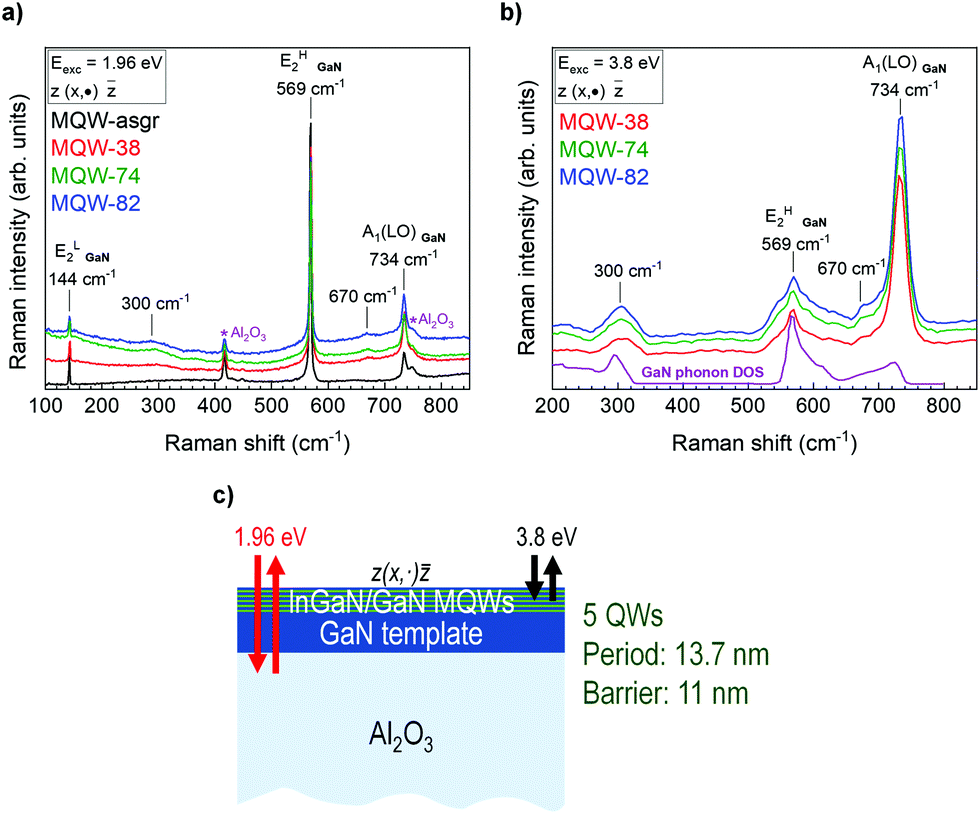 | ||
| Fig. 2 Raman spectra of the InGaN/GaN MQWs before and after Xe SHI irradiation obtained with (a) the 632.8 nm (1.96 eV) He–Ne laser line, and (b) the 325 nm (3.8 eV) He–Cd laser line. The calculated phonon DOS for GaN is included in (b).32 (c) Schematic representation of the Raman scattering geometry used in the experiments, as well as the penetration depth of 1.96 and 3.8 eV excitations. | ||
After irradiation, distinct features are noticed in the Raman spectrum: (i) increased background signal on the low-frequency side, (ii) two new broad bands peaking at 300 and 670 cm−1 attributed to disorder-activated vibrational modes, and (iii) allowed first order GaN phonons. The first two observations are intrinsically related to crystalline disorder with the broad bands being commonly observed in irradiated GaN structures. These bands have been attributed to disorder-activated Raman scattering of the highest acoustic-phonon branch mediated by isolated VGa, and to other vacancy type defects in the N sublattice, respectively.26,34,35 The existence of VGa defects had already been associated with irr-AB observed in the optical transmittance spectra (Fig. 1b). Notwithstanding the appearance of features associated with crystalline disorder in the spectra, first-order Raman scattering processes are dominant, suggesting that the crystalline structure of the sample as a whole was not seriously compromised. With increasing Se, the intensity ratio between the first-order Raman scattering processes and the background signal decreases, indicating an increase in the concentration of defects and/or scattering volume of the affected region. To the extent that irradiation-induced point defects introduce hydrostatic stress in crystals due to the expansion/contraction of the unit cell, it would be expected that a higher concentration of point defects would lead to a larger shift of the EH2 phonon.36 However, this is not the case observed here, indicating the Xe SHI irradiation does not modify the strain state of the GaN template, and thus its crystalline structure is not strongly disordered. This may explain why the spectra remain dominated by first-order processes, contrary to strongly disordered lattices for which the spectra evolve to the GaN phonon density of states (DOS).
Two possibilities can justify such behaviour: (i) the concentration of induced defects is low throughout the entire sample and only slightly increases with Se, or (ii) a thin region near the surface (a few tens of nanometres) is damaged, resulting in a higher concentration of defects at the surface, while the remaining sample is almost unaffected.
To elucidate both previous hypotheses, a μ-Raman study was performed using the 325 nm (3.8 eV) laser line. In this case, the optical absorption is high, causing the signal to come essentially from the upper region of the sample (about 40 nm – note the double absorption in backscattering geometry). Moreover, under this excitation, the Raman scattering occurs in a resonant condition with the electronic band states of GaN, which should lead to a strong enhancement of Raman scattering in the GaN barriers due to Fröhlich electron–phonon interaction, and consequently to an increase in the relative intensity of the polar A1(LO) phonon.37,38 Thus, with the used excitation conditions, it is possible to obtain information from the GaN barriers.
Fig. 2b shows the Raman spectra of the irradiated MQWs using the 325 nm (3.8 eV) laser line. For MQW-asgr, the GaN NBE luminescence hinders the detection of the Raman signal, not being possible to compare the spectra before and after irradiation. The calculated phonon density of states (DOS) for GaN is included for comparison.32 The two allowed phonons from GaN are detected at 569 cm−1 – EH2, and 734 cm−1 – A1(LO), with the relative intensity of the latter being favoured due to the resonance effect, as expected. Disorder-activated vibrational modes are observed at 300 and 670 cm−1. When comparing the spectra, it is possible to note an increase of the background signal when increasing the Xe SHI beam energy from 38 to 82 MeV. This corroborates our hypothesis about the slight increase in the concentration of defects with increasing Se.
Fig. 2c schematizes the geometry used in the Raman experiments, as well as the penetration depth of the 632.8 nm (1.96 eV) and 325 nm (3.8 eV) laser lines. When correlating the Raman spectra obtained with both laser lines, it is possible to notice that the main peaks are located at the same frequencies. However, the relative intensity of Raman peaks associated with the EH2 and A1(LO) phonons is different, the A1(LO) intensity being enhanced as expected due to the resonance process. Furthermore, under 3.8 eV excitation, the spectral shape is more similar to the GaN phonon DOS, reflecting the activation of the phonons from the entire Brillouin zone due to the scattering processes via defect mediation. These findings suggest that the surface region (the 40 nm probed) suffers higher damage, i.e. there is an increased density of irradiation-induced defects, while the rest of the sample is almost unaffected.
Given the InGaN reduced volume of scattering, 2.8 eV laser excitation was chosen to be as close as possible to the InGaN absorption tail, and so in resonance with an electronic state of the InGaN quantum wells.37,38 By using this experimental approach, the contribution from A1(LO)InGaN is expected to be intensified, making it possible to obtain information about the InGaN quantum-wells, which otherwise would be impossible. Nevertheless, this excitation is also resonant with the absorption band irr-AB at 2.75 eV (observed in Fig. 1b), which can hinder the detection of the signal from InGaN quantum-wells.
Fig. 3a shows the resonant Raman spectra of the MQWs after irradiation. For MQW-asgr, a strong luminescence contribution hampered the detection of the Raman signal, which prevents the comparison of the spectra before and after irradiation. After irradiation, it is possible to distinguish two peaks: (i) EH2GaN at 568 cm−1, and (ii) a broad band at approximately 730 cm−1 including contributions from InGaN, GaN, and sapphire.
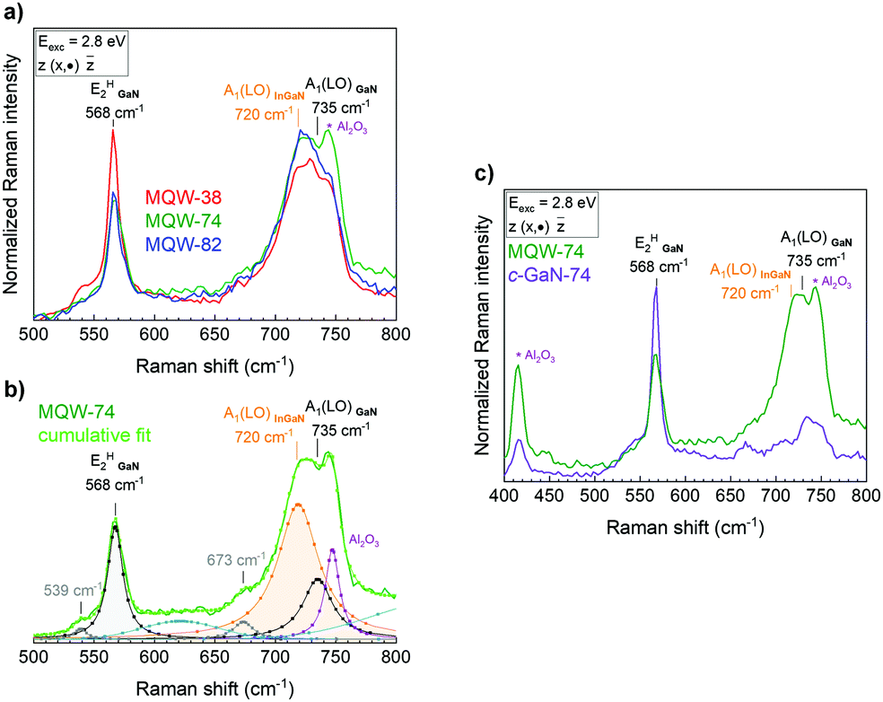 | ||
| Fig. 3 (a) Resonant Raman spectra of the Xe SHI irradiated InGaN/GaN MQWs using the 442 nm (2.8 eV) laser line. (b) Deconvolution procedure for the Raman peaks of MQW-74. (c) Comparison between the Raman spectra of 74 MeV Xe SHI irradiated c-plane GaN layers and MQWs using 2.8 eV excitation. | ||
A Lorentzian function deconvolution procedure was used to identify the distinct contributions present in the Raman spectra. An example of this process is shown in Fig. 3b for MQW-74. Two additional Gaussian functions were also considered in the deconvolution to better adjust the broad background contributions between 600 and 650 and above 750 cm−1. As a result of the deconvolution, it is possible to identify the EH2GaN and A1(LO)GaN phonons at 568 and 735 cm−1, respectively, related to both the barriers and/or the template. These values are (within the experimental error) comparable to those obtained with 3.8 and 1.96 eV excitations. Further features are detected, such as (i) a disorder-activated vibrational mode at 673 cm−1, and (ii) the A1g and Eg phonon modes at 418 and 750 cm−1, respectively, from the sapphire substrate.
The most interesting finding is now the possibility of identifying an intense peak at 720 cm−1 likely related to the A1(LO)InGaN phonon. To confirm the assignment of the 720 cm−1 Raman band it is necessary to identify the resonant channels responsible for the enhancement of this band. As the absorption band at 2.75 eV observed for irradiated MQWs is identical to the one observed for irradiated c-plane GaN layers (Fig. S1 in the ESI†),26 the Raman spectrum of c-plane GaN layers grown on sapphire and irradiated with 74 MeV Xe SHI was measured under the same experimental conditions (Fig. 3c). From this spectrum, it is possible to notice that the enhancement of A1(LO)GaN does not occur, although the excitation energy is resonant with irr-AB. Thus, it is possible to rule out the hypothesis that mid-gap states introduced by irradiation are involved in the resonance scattering process in GaN, with the related defects likely to be strongly localized, not relaxing through GaN lattice vibrations. The considerable enhancement of the 720 cm−1 Raman band in comparison to EH2GaN points to a resonance with the electronic levels of InGaN quantum wells.
According to Correia et al., it is not possible to distinguish In compositions, x, between 0.05 and 0.2 in pseudomorphic InGaN layers due to the opposite effects of composition and compressive stress, and the A1(LO)InGaN phonon is expected to be at ∼728–730 cm−1.38 Moreover, the critical layer thickness (CLT) for relaxation of InGaN layers with InN molar fractions below 0.25 is expected to be higher than 10 nm,39 hinting that the InGaN studied in this work grows pseudomorphically on GaN.
Considering both compositional and biaxial strain effects, the total expected shift of the A1(LO)InGaN phonon relative to A1(LO)GaN is given by Δω = Δωx + Δωs. Here, Δωx = −149x takes into account compositional effects;38 and  describes the effect of biaxial strain.40 Interpolating the values of the elastic constants C13 and C33 and the in-plane lattice parameter a for x = 0.15–0.30,41 and using the deformation potentials aλ and bλ reported for GaN,42 Δωs = (80 ± 3)x is obtained. Thus, the total shift Δω = 14 cm−1 corresponds to an x value of 0.20–0.22, which is compatible with the reported for pseudomorphic InGaN layers. However, it is important to note that the In composition in the quantum-wells may be slightly lower than that if they relax for thicknesses below the CLT as proposed by Lazić et al.40
Besides, looking at the intensity ratio between the A1(LO)InGaN and EH2GaN phonons, 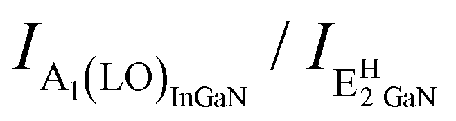 , an increase in the ratio is noted for higher irradiation energies (74 and 82 MeV). This points to a change in the resonance profile with the electronic state of the InGaN quantum wells approaching to match the excitation energy for higher irradiation energies. A change in the In/Ga ratio (i.e., the occurrence of intermixing at interfaces) can be involved in this process. In fact, for these irradiation energies, Se is higher than Seth,18,19 which can help to explain the occurrence of In/Ga intermixing along the track direction in the molten state, and in consequence the modification in the electronic resonance profile.
3.3. Rutherford backscattering spectrometry in channelling mode
To validate the previous findings, an independent RBS/C study was conducted. With this approach, it is possible to clarify the questions about the damage created by Xe SHI irradiation in the InGaN/GaN MQWs as well as the damage depth profile.Fig. 4 shows RBS/C spectra recorded along the 〈0001〉 direction of the InGaN/GaN MQWs before and after irradiation. A representative random (5° off-axis) RBS spectrum is also plotted. Using the McChasy software, the simulation of the random spectrum allows estimating the InN molar fraction to be 0.21 assuming a nominal quantum well thickness of 2.7 nm (consistent with X-ray diffraction measurements performed on the MQW-asgr sample – Fig. S2 in the ESI†). This value matches the In composition obtained by μ-Raman under 442 nm resonant excitation, confirming the validity of the methodology, and the analysis performed in Section 3.2.
 | ||
| Fig. 4 Aligned RBS/C spectra of the Xe SHI irradiated InGaN/GaN MQWs obtained along the 〈0001〉 direction. The random RBS spectrum is also included. Solid lines correspond to fits of the MC simulations performed using the McChasy code. The distinct energy windows used to measure χmin are indicated: (1) In signal from the MQWs; (2) Ga signal from the MQWs close to the surface; (3) Ga signal from the MQWs close to the GaN template; and (4) Ga signal from the first ∼120 nm of the GaN template. | ||
Moreover, from the RBS/C spectra it is possible to extract information about the crystalline quality of the samples by calculating the minimum yield (χmin), which is defined as the ratio of the RBS signal in the aligned spectrum to that of the random one within a region of interest. In this case, the signal from four energy windows was considered: (1) 1675–1745 keV, from In atoms localized within MQWs (measured at the full width at half-maximum); (2) 1580–1605 keV, from Ga atoms localized within the MQW region close to the surface; (3) 1533–1580 keV, from Ga atoms localized within the MQW region close to the interface with the GaN template; and (4) 1433–1533 keV, from Ga atoms localized within the first ∼120 nm of the GaN template. It is important to note that it is not possible to distinguish the Ga signal from the MQWs and the barriers.
The values of χmin are summarized in Table 2. Those referring to the MQW-asgr sample prove the high crystalline quality of the samples before irradiation.8 After irradiation, the minimum yield increases, and the introduced damage can be quantified by calculating the relative defect fraction (fD): fD = (χirraligned − χasgraligned)/χrandom, within the region of interest. These values are also included in Table 2.
| Sample | In (MQW) | Ga (MQW surface) | Ga (deeper in MQW) | Ga (GaN template) | ||||
|---|---|---|---|---|---|---|---|---|
| (1675–1745 keV) | (1675–1745 keV) | (1675–1745 keV) | (1675–1745 keV) | |||||
| χ min | f D | χ min | f D | χ min | f D | χ min | f D | |
| MQW-asgr | 3.2 ± 0.2 | — | 6.6 ± 0.3 | — | 2.8 ± 0.2 | — | 2.7 ± 0.2 | — |
| MQW-38 | 5.2 ± 0.3 | 1.9 ± 0.2 | 8.9 ± 0.3 | 2.3 ± 0.2 | 4.4 ± 0.3 | 1.6 ± 0.2 | 4.4 ± 0.3 | 1.7 ± 0.2 |
| MQW-74 | 5.4 ± 0.3 | 2.1 ± 0.2 | 8.6 ± 0.3 | 2.0 ± 0.2 | 4.2 ± 0.2 | 1.5 ± 0.2 | 4.2 ± 0.3 | 1.4 ± 0.2 |
| MQW-82 | 5.7 ± 0.3 | 2.5 ± 0.2 | 10.1 ± 0.4 | 3.5 ± 0.2 | 4.6 ± 0.3 | 1.7 ± 0.2 | 4.6 ± 0.3 | 1.9 ± 0.2 |
Despite the different Xe SHI energies, only the relative defect fraction of the Ga-window lying close to the surface suggests a significant increase of the damage for the highest energy. This agrees with recent Molecular Dynamics (MD) simulations of Xe SHI irradiation of c-plane GaN layers in the same energy region. Indeed, increased damage at the surface was found to a depth of 5 and 18 nm for energies of 45 and 70 MeV, respectively.43 Slightly higher defect levels are seen for the In signal compared to the Ga signal from the deeper region of the MQWs, suggesting that the InGaN MQWs suffer higher damage than the GaN barriers. Similar results were observed for low energy ion implantation in InGaN/GaN MQWs.44 The damage levels of GaN in a deeper region of the MQWs and the GaN template are similar within the uncertainties.
To understand the damage profile in more detail, MC simulations were carried out. The corresponding depth distributions of defects, modelled as randomly displaced atoms (RDAs), are shown in Fig. 5. For all the Xe SHI energies, defects are dominant at the surface, corroborating the previous assumptions made from μ-Raman spectroscopy.
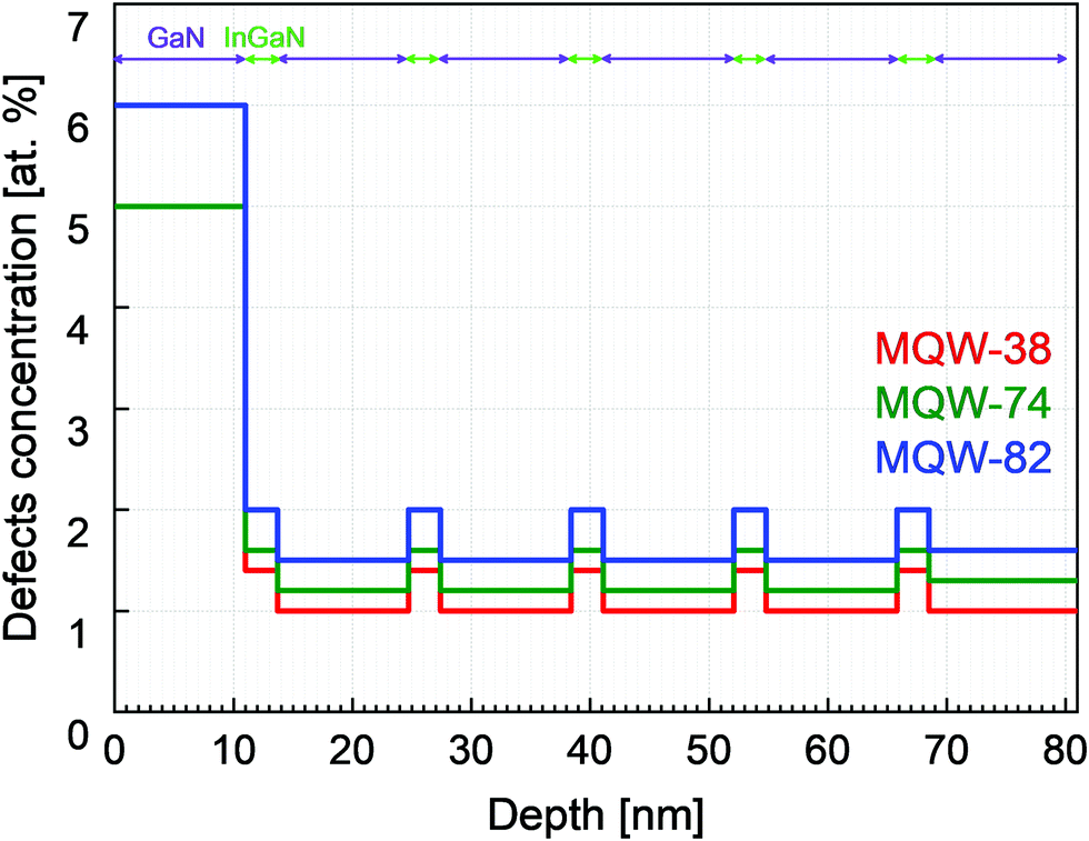 | ||
| Fig. 5 Depth-distribution of defects in the InGaN/GaN MQW region for the irradiated samples as obtained from the MC simulation by the McChasy code. | ||
For samples MQW-74 and MQW-82, in addition to RDAs, a small density of dislocations (1 × 109 cm−2 and 1.5 × 109 cm−2, respectively) was assumed in the GaN template to fit well the increasing Ga-backscattering yield at lower energies of the RBS/C spectra. The formation of dislocations in GaN irradiated with Xe SHI in this range of energies agrees with MD simulations.43
The RBS/C analysis not only confirms the μ-Raman discussion but also quantifies the damage created in the InGaN/GaN MQWs. However, RBS/C does not give information about the lateral distribution of the defects; it only provides their average concentration at a given depth. It means that the defects are not necessarily distributed uniformly throughout the direction parallel to the surface.
3.4. Photoluminescence and photoluminescence excitation
In order to obtain information about the localization of the emitting states of the InGaN/GaN MQWs before and after irradiation and their respective excitation mechanisms, the PL and PLE techniques were used.Fig. 6 depicts RT PL spectra of the MQW-asgr, MQW-38, and MQW-82 samples when exciting above the GaN bandgap energy (3.8 eV). For MQW-asgr, the PL spectrum reveals the GaN NBE emission at 3.4 eV and a broad and intense yellow band (YB) with a maximum at about 2.3 eV. The YB emission is modulated by optical interference caused by the superposition of multiple reflections in the GaN-based film. Under these experimental conditions, after irradiation, it becomes impossible to detect any luminescence. Such extinction in the PL intensity corroborates the assumption about the crystalline disorder induced in the GaN barriers discussed in Section 3.2 and 3.3. Further on, the PL response for other excitation energies will be discussed in detail.
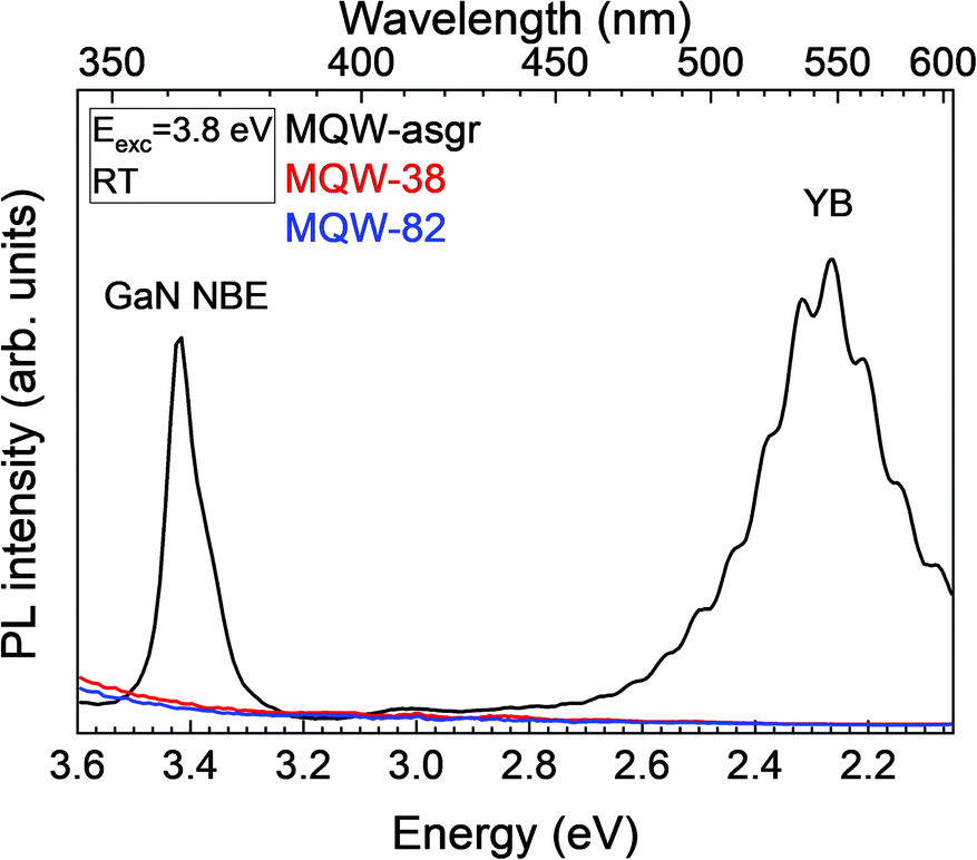 | ||
| Fig. 6 RT PL spectra (excitation energy of 3.8 eV) of the MQW-asgr, MQW-38, and MQW-82 samples. The tail in the spectra of the irradiated samples is observed due to direct excitation light. | ||
It is important to note that distinct contributions can participate in the YB luminescence, namely InGaN excitonic emission and optically active defects in GaN or InGaN. To distinguish them, the PLE technique was used, monitoring the YB emission at different wavelengths.
Fig. 7a shows the normalized PLE spectra monitored at different YB emission energies for the MQW-asgr sample. Two excitation mechanisms can be distinguished: (i) the GaN absorption edge at high energies and (ii) an excitation tail at low energies due to InGaN absorption.
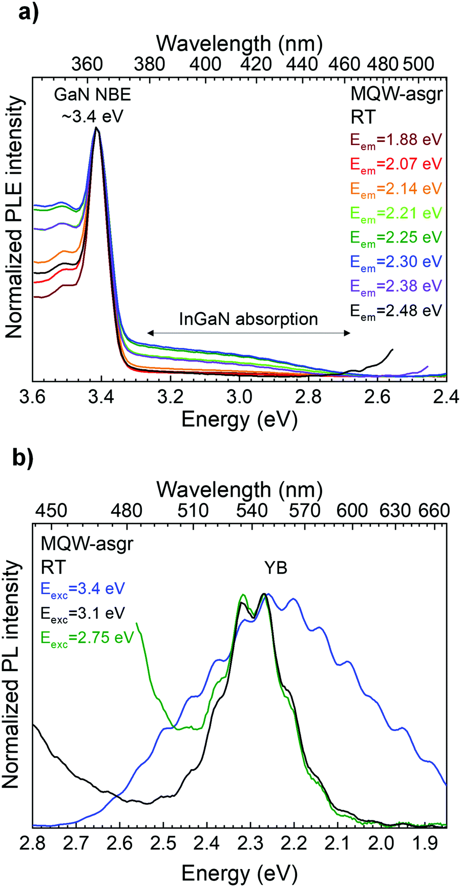 | ||
| Fig. 7 (a) RT PLE spectra of MQW-asgr monitoring at different emission energies of the YB. (b) RT PL spectra of MQW-asgr obtained with different excitation energies: at the GaN bandgap (3.4 eV), and below the GaN bandgap (3.1 eV and 2.75 eV). | ||
Although the entire YB emission is excited through the GaN band edge, the same does not occur for the second mechanism. In the latter case, only a narrow emission band, between 2.2 and 2.4 eV, is excited through InGaN. The changes in the spectral shape of the YB when the sample is excited with different energies can be better analyzed in Fig. 7b. This result implies that at least two contributions are involved in this luminescence, one of them likely involving localized excitons in InGaN and the other one related to deep level defects in GaN. In undoped GaN, such emission is most often attributed to carbon-related defects.45–47 The presence of carbon and oxygen impurities, although unintentional, is common in undoped III–N semiconductors grown by MOVPE, being introduced either from the precursors and/or from the release of gases from the reactor components.48 Nevertheless, given the complexity of the YB, the involvement of other kinds of defects for this emission cannot be excluded, particularly those involving VGa and/or associated complexes.27,28,49–51
From Fig. 7b, it is noted that the InGaN excitonic emission peaks at 2.3 eV. Considering the correlation between the InGaN effective bandgap energy (Eeffg) and the emission maximum (EPL) observed by O’Donnell et al. for different types of InGaN structures (EPL = 1.45Eeffg − 1.54),52Eeffg = 2.65 eV. This value closely matches the onset of the absorption tail. Considering not only compositional effects but also that InGaN grows pseudomorphically on GaN, an InN molar fraction of 0.23–0.24 is estimated considering the following expression: Eeffg = 0.7x + 3.4(1 − x) − 1.65x(1 − x) + 0.79x.53 However, it is important to consider that, in MQWs, the PL peak energy may be redshifted due to the QCSE,54 and the existence of In compositional fluctuations in the wells.55 These effects may result in an overestimation of the In composition through the used method.
Returning to Fig. 6, it is important to understand the reason for the YB extinction and if it is due to Xe SHI irradiation or different excitation mechanisms. Therefore, PLE spectra were acquired at distinct energies of the YB (considering a similar spectral range to that of MQW asgr). Fig. 8a shows the RT PLE spectra for the MQW-82 sample, being confirmed that the YB emission is not quenched at all. However, the excitation of the YB is distinct after irradiation, not being possible to excite it with an energy equal to or above the GaN band edge. Xe SHI irradiation was already seen to generate defects in the first nanometers of the sample (with greater preponderance in the first GaN barrier – see Fig. 5). Such defects can introduce energy levels in the GaN mid-gap and act as traps for electrons (holes) optically excited to the GaN conduction (valence) band. Their presence increases nonradiative recombination channels,56–58 which may explain why it is not possible to detect any luminescence, with the experimental conditions used, in the UV/visible spectral region when GaN band-to-band excitation is carried out.
 | ||
| Fig. 8 (a) RT PLE spectra of the MQW-82 sample monitored at different emission energies along with the YB. (b) RT PLE spectra of MQW-asgr, MQW-38, and MQW-82 at 2.25 eV. The spectra were normalized to the maximum of irr-AB, for the irradiated samples, and to the PLE intensity at 3.1 eV, for MQW-asgr. (c) RT PL spectra of the MQW-asgr, MQW-38, and MQW-82 samples when exciting at 2.75 eV and of MQW-asgr when exciting at 3.4 eV. The spectra were vertically shifted for clarity. | ||
Nevertheless, after Xe SHI irradiation, there are other defects formed in GaN with mid-gap energy levels, namely the one that can absorb light with energy below the GaN bandgap (irr-AB at 2.75 eV, previously observed in optical transmittance, Fig. 1b). In this case, the excitation of the contribution of the YB due to defects in GaN is possible, revealing that irradiation introduces a new excitation channel for the YB emission. By varying the excitation along irr-AB, the spectral shape of the YB does not change (not shown). It should be mentioned that the absorption through InGaN may be overlapped with irr-AB, hindering the identification of the InGaN absorption onset and, consequently, the possible detection of deviations from it resulting from intermixing at InGaN/GaN interfaces, as inferred by μ-Raman spectroscopy.
The comparison between the YB excitation processes before and after Xe SHI irradiation can be seen more clearly in Fig. 8b. Here, it is possible to identify that, after irradiation, the preferential excitation pathway for the YB is through the absorption band generated at 2.75 eV, independently of the SHI energy loss (within the range studied).
Fig. 8c shows the normalized RT PL spectra of the MQW-asgr, MQW-38, and MQW-82 samples when exciting with 2.75 eV photon energy. This energy corresponds to excitation through InGaN and irr-AB (for irradiated samples only). The PL spectrum of MQW-asgr under 3.4 eV excitation is also included in Fig. 8c. Despite the strong quenching of the intensity (more than one order of magnitude) and differences in the excitation mechanisms of the YB emission, the spectral shape of the YB after irradiation is analogous to that of the MQW-asgr sample for excitation above the bandgap. This suggests that the contributions to the YB luminescence remain identical, not being possible to distinguish the excitonic contribution of InGaN (as in MQW-asgr) and the contributions related to other deep-level defects.
4. Conclusions
In summary, the effects of Xe SHI irradiation with energies between 38 and 82 MeV on the optical and structural properties of InGaN/GaN MQWs were explored. A profile of the damage introduced by irradiation in this structure was identified using μ-Raman spectroscopy. Through the proper use of this technique, by combining different excitation energies under resonant and non-resonant conditions, it was found that the sample's surface is the most affected region, i.e., in this region there exists a higher concentration of defects, which affects both the crystalline structure and the luminescence properties of the MQWs. It was noticed that the damage introduced only slightly increases with the Xe SHI energy. The in-depth damage profile was further corroborated by RBS/C measurements and MC simulations. Nevertheless, the irradiation energy was found to change the Raman resonance profile in InGaN, as evidenced by the increase in the intensity ratio for higher irradiation energies (74 and 82 MeV). This is likely related to the existence of intermixing at the MQWs’ interfaces, due to the diffusion of Ga and In atoms in the molten state reached in the passage of swift-heavy ions in the structure.
PL/PLE experiments allowed us to distinguish two contributions for the YB in the MQW-asgr sample by controlling the excitation/emission energy. Those contributions were related to (i) InGaN excitonic emission; and (ii) emission in GaN-related deep-level defects. After irradiation, an electronic mid-gap state (responsible for irr-AB at 2.75 eV), able to absorb light in the same energy region of the InGaN absorption tail, was found to participate in the excitation of GaN-related defect YB emission, which was no longer possible to excite with energy above the GaN bandgap. It would not have been possible to discern the distinct YB contributions (and consequently In/Ga intermixing) after irradiation due to the overlap of the InGaN absorption edge with irr-AB by PL/PLE.
Considering the results, it is possible to infer that, from a technological point of view, the use of SHI to obtain intermixing in InGaN/GaN MQWs might be compromised by the introduction of defects detrimental to the light emission efficiency. The use of post-irradiation treatments will be further studied as a possible approach to remove these defects.
Conflicts of interest
There are no conflicts to declare.Acknowledgements
This work was supported by the project “Nano-engineering of wide bandgap semiconductors using ion beams” (NASIB) by FCT (Portuguese Foundation for Science and Technology) and FEDER (POCI-01-0145-FEDER-028011 and LISBOA-01-0145-FEDER-02966). This work was developed within the scope of the project i3N (UIDB/50025/2020 and UIDP/50025/2020) and INESC MN (UID/05367/2020) financed by national funds through the FCT/MEC. J. Cardoso acknowledges the PhD grant DAEPHYS-FCT PD/BD/142780/2018 financed by the European Social Fund (FSE) and national funds of FCT/MCTES. The irradiation experiments were performed at the Grand Accélérateur National d’Ions Lourds (GANIL), Caen, France, and the authors thank the CIMAP, the CIRIL and GANIL staff for their help.References
- S. Nakamura, Rev. Mod. Phys., 2015, 87, 1139–1151 CrossRef.
- Y. Narukawa, J. Narita, T. Sakamoto, T. Yamada, H. Narimatsu, M. Sano and T. Mukai, Phys. Status Solidi A, 2007, 204, 2087–2093 CrossRef.
- E. Kioupakis, Q. Yan and C. G. Van De Walle, Appl. Phys. Lett., 2012, 101, 1–6 CrossRef.
- K. P. O’Donnell, M. Auf der Maur, A. di Carlo and K. Lorenz, Phys. Status Solidi RRL, 2012, 6, 49–52 CrossRef.
- M. Auf der Maur, A. Pecchia, G. Penazzi, W. Rodrigues and A. Di Carlo, Phys. Rev. Lett., 2016, 116, 027401 CrossRef PubMed.
- M. Auf Der Maur, K. Lorenz and A. Di Carlo, Opt. Quantum Electron., 2012, 44, 83–88 CrossRef.
- S.-H. Han, D.-Y. Lee, H.-W. Shim, G.-C. Kim, Y. S. Kim, S.-T. Kim, S.-J. Lee, C.-Y. Cho and S.-J. Park, J. Phys. D: Appl. Phys., 2010, 43, 354004 CrossRef.
- K. Lorenz, A. Redondo-Cubero, M. B. Lourenço, M. C. Sequeira, M. Peres, A. Freitas, L. C. Alves, E. Alves, M. P. Leitão, J. Rodrigues, N. Ben Sedrine, M. R. Correia and T. Monteiro, in Proceeding of SPIE - Gallium Nitride Materials and Devices XI, ed. J.-I. Chyi, H. Fujioka, H. Morkoç, Y. Nanishi, U. T. Schwarz and J.-I. Shim, 2016, vol. 9748, p. 97480L Search PubMed.
- C. C. Chuo, C. M. Lee and J. I. Chyi, Appl. Phys. Lett., 2001, 78, 314–316 CrossRef.
- M. D. McCluskey, L. T. Romano, B. S. Krusor, N. M. Johnson, T. Suski and J. Jun, Appl. Phys. Lett., 1998, 73, 1281–1283 CrossRef.
- M. A. Sousa, T. C. Esteves, N. Ben Sedrine, J. Rodrigues, M. B. Lourenço, A. Redondo-Cubero, E. Alves, K. P. O’Donnell, M. Bockowski, C. Wetzel, M. R. Correia, K. Lorenz and T. Monteiro, Sci. Rep., 2015, 5, 6–11 Search PubMed.
- D. K. Avasthi and G. K. Mehta, Swift Heavy Ions for Materials Engineering and Nanostructuring, Springer, Netherlands, Dordrecht, 2011, vol. 145 Search PubMed.
- S. Kraft, B. Schattat, W. Bolse, S. Klaumünzer, F. Harbsmeier, A. Kulinska and A. Löffl, J. Appl. Phys., 2002, 91, 1129–1134 CrossRef.
- W. Bolse, B. Schattat and A. Feyh, Appl. Phys. A: Mater. Sci. Process., 2003, 77, 11–15 CrossRef.
- F. F. Komarov, Usp. Fiz. Nauk, 2017, 187, 465–504 CrossRef.
- W. J. Weber, D. M. Duffy, L. Thomé and Y. Zhang, Curr. Opin. Solid State Mater. Sci., 2015, 19, 1–11 CrossRef.
- M. Lang, F. Djurabekova, N. Medvedev, M. Toulemonde and C. Trautmann, Reference Module in Materials Science and Materials Engineering, Elsevier, 2020, pp. 1–73 Search PubMed.
- M. Sall, I. Monnet, F. Moisy, C. Grygiel, S. Jublot-Leclerc, S. Della–Negra, M. Toulemonde and E. Balanzat, J. Mater. Sci., 2015, 50, 5214–5227 CrossRef.
- F. Moisy, M. Sall, C. Grygiel, A. Ribet, E. Balanzat and I. Monnet, Nucl. Instrum. Methods Phys. Res., Sect. B, 2018, 431, 12–18 CrossRef.
- M. Karlušić, R. Kozubek, H. Lebius, B. Ban-d’Etat, R. A. Wilhelm, M. Buljan, Z. Siketić, F. Scholz, T. Meisch, M. Jakšić, S. Bernstorff, M. Schleberger and B. Šantić, J. Phys. D: Appl. Phys., 2015, 48, 325304 CrossRef.
- M. Ali, O. Svensk, Z. Zhen, S. Suihkonen, P. T. Törmä, H. Lipsanen, M. Sopanen, K. Hjort and J. Jensen, Phys. B, 2009, 404, 4925–4928 CrossRef CAS.
- K. Prabakaran, R. Ramesh, M. Jayasakthi, S. Surender, S. Pradeep, M. Balaji, K. Asokan and K. Baskar, Nucl. Instrum. Methods Phys. Res., Sect. B, 2017, 394, 81–88 CrossRef CAS.
- J. F. Ziegler, J. P. Biersack and M. D. Ziegler, SRIM: The stopping and range of ions in matter, SRIM Co., Chester, Maryland, 2008 Search PubMed.
- P. Jozwik, L. Nowicki, R. Ratajczak, C. Mieszczynski, A. Stonert, A. Turos, K. Lorenz and E. Alves, Advanced Monte Carlo Simulations for Ion-Channeling Studies of Complex Defects in Crystals, in Theory and Simulation in Physics for Materials Applications, ed. E. Levchenko, Y. Dappe and G. Ori, Springer Series in Materials Science, Springer, Cham, 2020, vol. 296 Search PubMed.
- P. Jozwik, L. Nowicki, R. Ratajczak, A. Stonert, C. Mieszczynski, A. Turos, K. Morawiec, K. Lorenz and E. Alves, J. Appl. Phys., 2019, 126, 195107 CrossRef.
- F. Moisy, M. Sall, C. Grygiel, E. Balanzat, M. Boisserie, B. Lacroix, P. Simon and I. Monnet, Nucl. Instrum. Methods Phys. Res., Sect. B, 2016, 381, 39–44 CrossRef CAS.
- J. L. Lyons, A. Alkauskas, A. Janotti and C. G. Van de Walle, Phys. Status Solidi, 2015, 252, 900–908 CrossRef CAS.
- J. L. Lyons and C. G. Van De Walle, npj Comput. Mater., 2017, 3, 1–9 CrossRef CAS.
- T. Ruf, Phonon Raman Scattering in Semiconductors, Quantum Wells and Superlattices, Springer-Verlag, Berlin Heidelberg, Germany, 1998 Search PubMed.
- C. A. Arguello, D. L. Rousseau and S. P. S. Porto, Phys. Rev., 1969, 181, 1351–1363 CrossRef CAS.
- M. Kuball, Surf. Interface Anal., 2001, 31, 987–999 CrossRef CAS.
- V. Y. Davydov, Y. E. Kitaev, I. N. Goncharuk, A. N. Smirnov, J. Graul, O. Semchinova, D. Uffmann, M. B. Smirnov, A. P. Mirgorodsky and R. A. Evarestov, Phys. Rev. B: Condens. Matter Mater. Phys., 1998, 58, 12899–12907 CrossRef CAS.
- S. Strite, J. Vac. Sci. Technol., B: Microelectron. Nanometer Struct.--Process., Meas., Phenom., 1992, 10, 1237 CrossRef CAS.
- M. Katsikini, K. Papagelis, E. C. Paloura and S. Ves, J. Appl. Phys., 2003, 94, 4389–4394 CrossRef CAS.
- B. S. Li and Z. G. Wang, J. Phys. D: Appl. Phys., 2015, 48, 225101 CrossRef.
- C. Kisielowski, J. Krüger, S. Ruvimov, T. Suski, J. Ager, E. Jones, Z. Liliental-Weber, M. Rubin, E. Weber, M. Bremser and R. Davis, Phys. Rev. B: Condens. Matter Mater. Phys., 1996, 54, 17745–17753 CrossRef CAS.
- M. R. Correia, S. Pereira, T. Monteiro, E. Pereira and E. Alves, MRS Proc., 2000, 639, G6.10 CrossRef.
- M. R. Correia, S. Pereira, E. Pereira, J. Frandon and E. Alves, Appl. Phys. Lett., 2003, 83, 4761–4763 CrossRef CAS.
- S. Pereira, M. R. Correia, E. Pereira, C. Trager-Cowan, F. Sweeney, K. P. O’Donnell, E. Alves, N. Franco and A. D. Sequeira, Appl. Phys. Lett., 2002, 81, 1207–1209 CrossRef CAS.
- S. Lazić, M. Moreno, J. M. Calleja, A. Trampert, K. H. Ploog, F. B. Naranjo, S. Fernandez and E. Calleja, Appl. Phys. Lett., 2005, 86, 1–3 CrossRef.
- I. Vurgaftman, J. R. Meyer and L. R. Ram-Mohan, J. Appl. Phys., 2001, 89, 5815–5875 CrossRef CAS.
- J. M. Wagner and F. Bechstedt, Appl. Phys. Lett., 2000, 77, 346–348 CrossRef CAS.
- M. C. Sequeira, J.-G. Mattei, H. Vazquez, F. Djurabekova, K. Nordlund, I. Monnet, P. Mota-Santiago, P. Kluth, C. Grygiel, S. Zhang, E. Alves and K. Lorenz, Commun. Phys., 2021, 4, 51 CrossRef CAS.
- A. Redondo-Cubero, K. Lorenz, E. Wendler, S. Magalhães, E. Alves, D. Carvalho, T. Ben, F. M. Morales, R. García, K. P. O’Donnell and C. Wetzel, Nanotechnology, 2015, 26, 425703 CrossRef CAS PubMed.
- J. L. Lyons, A. Janotti and C. G. Van de Walle, Appl. Phys. Lett., 2010, 97, 152108 CrossRef.
- M. A. Reshchikov, J. D. McNamara, H. Helava, A. Usikov and Y. Makarov, Sci. Rep., 2018, 8, 1–11 CAS.
- M. A. Reshchikov, M. Vorobiov, D. O. Demchenko, Ü. Ozgur, H. Morkoç, A. Lesnik, M. P. Hoffmann, F. Hörich, A. Dadgar and A. Strittmatter, Phys. Rev. B, 2018, 98, 125207 CrossRef CAS.
- I. M. Watson, Coord. Chem. Rev., 2013, 257, 2120–2141 CrossRef CAS.
-
M. A. Reshchikov and H. Mork
![[o with combining cedilla]](https://www.rsc.org/images/entities/char_006f_0327.gif) , J. Appl. Phys., 2005, 97, 1–95 Search PubMed.
, J. Appl. Phys., 2005, 97, 1–95 Search PubMed. - A. Sedhain, J. Li, J. Y. Lin and H. X. Jiang, Appl. Phys. Lett., 2010, 96, 151902 CrossRef.
- N. Ben Sedrine, T. C. Esteves, J. Rodrigues, L. Rino, M. R. Correia, M. C. Sequeira, A. J. Neves, E. Alves, M. Bockowski, P. R. Edwards, K. P. O’Donnell, K. Lorenz and T. Monteiro, Sci. Rep., 2015, 5, 3–9 Search PubMed.
- K. P. O’Donnell, J. F. W. Mosselmans, R. W. Martin, S. Pereira and M. E. White, J. Phys.: Condens. Matter, 2001, 13, 6977–6991 CrossRef.
- E. Sakalauskas, Ö. Tuna, A. Kraus, H. Bremers, U. Rossow, C. Giesen, M. Heuken, A. Hangleiter, G. Gobsch and R. Goldhahn, Phys. Status Solidi B, 2012, 249, 485–488 CrossRef CAS.
- O. Ambacher, J. Majewski, C. Miskys, A. Link, M. Hermann, M. Eickhoff, M. Stutzmann, F. Bernardini, V. Fiorentini, V. Tilak, B. Schaff and L. F. Eastman, J. Phys.: Condens. Matter, 2002, 14, 3399–3434 CrossRef CAS.
- D. Carvalho, F. M. Morales, T. Ben, R. García, A. Redondo-Cubero, E. Alves, K. Lorenz, P. R. Edwards, K. P. O’Donnell and C. Wetzel, Microsc. Microanal., 2015, 21, 994–1005 CrossRef CAS.
- W. Shockley and W. T. Read, Phys. Rev., 1952, 87, 835–842 CrossRef CAS.
- R. N. Hall, Phys. Rev., 1952, 87, 387 CrossRef CAS.
- T. Goudon, V. Miljanović and C. Schmeiser, SIAM J. Appl. Math., 2007, 67, 1183–1201 CrossRef.
Footnote |
| † Electronic supplementary information (ESI) available. See DOI: 10.1039/d1tc01603b |
| This journal is © The Royal Society of Chemistry 2021 |