
 Open Access Article
 This Open Access Article is licensed under a
 Creative Commons Attribution 3.0 Unported Licence
Halide perovskites scintillators: unique promise and current limitations†
Oliver D. I.
Moseley
 a,
Tiarnan A. S.
Doherty
a,
Richard
Parmee
b,
Miguel
Anaya
*ac and
Samuel D.
Stranks
*ac
a,
Tiarnan A. S.
Doherty
a,
Richard
Parmee
b,
Miguel
Anaya
*ac and
Samuel D.
Stranks
*ac
aCavendish Laboratory, University of Cambridge, JJ Thomson Avenue, Cambridge CB3 0HE, UK. E-mail: sds65@cam.ac.uk; ma811@cam.ac.uk
bCheyney Design and Development, Ltd., Litlington, Cambridge, SG8 0SS, UK
cDepartment of Chemical Engineering & Biotechnology, University of Cambridge, Philippa Fawcett Drive, Cambridge CB3 0AS, UK
First published on 1st June 2021
Abstract
The widespread use of X- and gamma-rays in a range of sectors including healthcare, security and industrial screening is underpinned by the efficient detection of the ionising radiation. Such detector applications are dominated by indirect detectors in which a scintillating material is combined with a photodetector. Halide perovskites have recently emerged as an interesting class of semiconductors, showing enormous promise in optoelectronic applications including solar cells, light-emitting diodes and photodetectors. Here, we discuss how the same superior semiconducting properties that have catalysed their rapid development in these optoelectronic devices, including high photon attenuation and fast and efficient emission properties, also make them promising scintillator materials. By outlining the key mechanisms of their operation as scintillators, we show why reports of remarkable performance have already emerged, and describe how further learning from other optoelectronic devices will propel forward their applications as scintillators. Finally, we outline where these materials can make the greatest impact in detector applications by maximally exploiting their unique properties, leading to dramatic improvements in existing detection systems or introducing entirely new functionality.
 Miguel Anaya | Miguel Anaya is a Research Fellow at Darwin College and a Leverhulme Early Career Fellow in the Department of Chemical Engineering and Biotechnology at the University of Cambridge. He completed his PhD at the Spanish National Research Council in 2018, with recognition from the GEFES/Spanish Royal Society of Physics as the best Thesis in Experimental Physics. He leads a subgroup at the StranksLab focused on the modeling, fabrication, and characterization of perovskite-based light-emitting devices and sensors. |
1. Introduction
Ionising radiation in the form of X- and gamma-rays are powerful modern diagnostic tools. These energetic photons, typically kiloelectron volts and above, exhibit long penetration depths that exceed the millimetre scale1 (Fig. 1a) and enable a diverse range of applications, including healthcare,2 industrial screening,3,4 non-destructive imaging,5 spectroscopy,6 astronomy,7,8 and security.9 The usefulness of ionising radiation is dependent on the radiation source, the sample, the associated interface electronics, dedicated image processing algorithms and, crucially, the radiation detector itself.10 Solid-state radiation detection can be split into two distinct categories, direct and indirect, which differ in the way they generate a signal from the incident radiation (Fig. 1b and c). Direct detectors harvest the incident radiation and produce energised charge carriers, which are extracted by electrodes to generate a signal (Fig. 1b).11 Despite the relative simplicity of such devices, their commercial application is hindered by the constraints imposed by deeply penetrating radiation. Charge collection distances have to be on the order of the material thickness, and as the radiation energy increases above 40 keV and typical absorption depths exceed the millimeter scale, efficient and fast charge extraction becomes difficult. Consequently, direct detection is only employed for soft X-rays due to their shorter penetration depths, for example in mammography utilizing < 40 keV X-rays2 and medical device inspection.12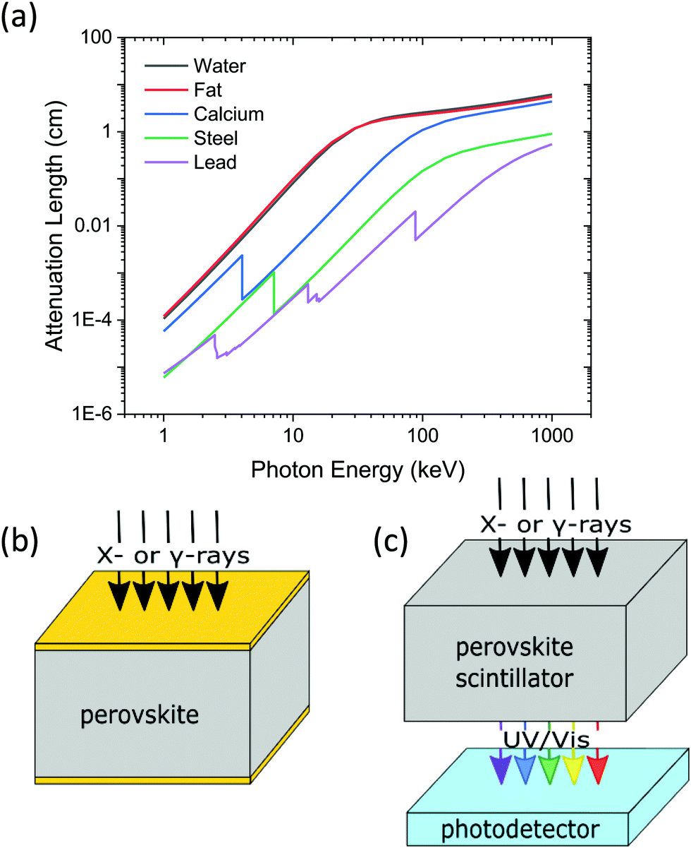 | ||
| Fig. 1 (a) The strong increase in absorption length as photon energy increases for a range of materials. The fat (red) component represents a common triglyceride molecule common in animal fat cells. The difference in absorption between calcium in bones and organics in tissue enables contrast images to be generated. (b and c) Schematics of (b) direct and (c) indirect detection mechanisms. In the case of direct detectors, metal electrodes are employed to extract generated charge carriers to produce the signal. For indirect detectors, the incident beam impinges on the scintillator material and generates UV/Vis photons, which are then collected by a photodetector to produce the signal. | ||
Indirect detectors involve a radiation-sensitive material that down-converts the incident beam into UV/Vis light, which is then collected by an array of sensitive photodetectors, such as PIN diodes or photomultiplier tubes. This emissive material is known as a scintillator, and the light produced from ionising radiation excitation is radioluminescence (RL). Given there are no long-range charge collection requirements, scintillators can retain detection properties when the material thickness exceeds millimeters, enabling use across the whole X- and gamma-ray spectrum. Furthermore, decoupling the detection process into two distinct steps permits each to be optimized separately, allowing decades of advancements in photodetector development to be exploited. Fast scintillator emission is suitable for high-speed applications13 and high imaging frame rates, with the sub-nanosecond RL decay times achievable far exceeding the charge collection times in direct detectors.14,15 As a result, indirect detectors dominate applications, from medical radiography to particle collider calorimeters. However, typical commercial scintillators, such as CsI:Tl, are hindered by their high production costs and fixed emission wavelengths, limiting their functionality with substrates and detectors. Furthermore, the diverse range of applications makes it near-impossible to produce a one-size-fits-all scintillator. Developing new detectors with increased functionality and performance is of great importance, especially in medical imaging, where the benefits of the procedure must be carefully balanced against the increased risk of cancer associated with patient radiation exposure.16 Whilst existing techniques, such as conventional transmission radiography, can provide useful diagnostic information at safe dose levels, more advanced techniques require the patients to be monitored to ensure that cumulative dose does not exceed safe limits. This is particularly important for the increasing use of computed tomography (CT, 5 million yearly scans in the UK alone17), with each scan administering up to 10 mSv (equivalent to 4.5 years of natural background radiation);18 low dose radiography will be very advantageous for such applications.
Recently, a unique class of semiconductors, halide perovskites (PVKs) have demonstrated a series of breakthroughs in a range of optoelectronic applications. Most notably, PVK solar cells have reached power conversion efficiencies of over 25% in little more than a decade,19 owing to strong direct band gap absorption, excellent charge transport properties and high defect tolerance.20 Together with these ideal optoelectronic properties, the high atomic weight of the constituent elements render PVKs promising candidates for ionising radiation detector materials. PVKs were demonstrated as a direct detector material following the synthesis of millimeter-sized single crystals, with X-ray-induced currents reported in CsPbBr321 and MAPbI322 (MA = methylammonium) crystals, and improvements in crystal quality23 and device integration24 advanced the field quickly. PVK direct detectors have achieved ultralow detection limits (<10 nGys−1)25,26 and up to 100 times the sensitivity of their a-Se counterpart27 for soft X-rays, making them exciting commercial prospects. However, high dark currents of 23 nA cm−2![[thin space (1/6-em)]](https://www.rsc.org/images/entities/char_2009.gif) 27 even under small external fields remain a problem for direct PVK detectors, in part due to the low bulk resistivity and the bias instabilities caused by ion migration. Growth methods,28 compositional engineering,29 passivation30 and dimensionality tuning31 are all promising solutions to these issues. The reader is referred to a comprehensive review of PVKs for direct detection.32
27 even under small external fields remain a problem for direct PVK detectors, in part due to the low bulk resistivity and the bias instabilities caused by ion migration. Growth methods,28 compositional engineering,29 passivation30 and dimensionality tuning31 are all promising solutions to these issues. The reader is referred to a comprehensive review of PVKs for direct detection.32
PVKs were first proposed as scintillators in the 1990s,33–36 an application revived in the last few years following great success of PVKs as light emitters with high photoluminescence quantum efficiencies and colour control from band gap and dimensionality tuning. Recently, scintillation has been demonstrated in a range of PVKs from bulk crystals37 to nanocrystals,38,39 and they remain an exciting prospect to offer sub-nanosecond emission with high light yields from a material that can be synthesised inexpensively and at low temperatures. The rapid advancement of PVK scintillators, already outperforming some commercial materials, combined with the dominance of indirect systems in practical detector applications has generated industrial interest in the materials.40 Herein, we dissect the operating mechanisms and advantages of PVKs in indirect detectors, highlighting areas where they can replace traditional materials, or offer unique properties that can be exploited. The limitations of PVKs are discussed, and pathways to further improve the materials are proposed, utilising ongoing knowledge derived from the concurrent development of other PVK optoelectronic devices. Finally, applications where PVKs may find unique commercial use are outlined.
2. General scintillator considerations
2.1 Mechanism
While the exact mechanisms of RL are complex and material-dependent, the general process can be simplified into three key steps: (i) generation and relaxation of excited charge carriers, (ii) transport of carriers to emission centres, and (iii) radiative recombination of carriers (Fig. 2). A prediction for the maximum number of photons emitted (Nph) is possible by looking at each of these steps in eqn (1):| Nph = B × S × Q | (1) |
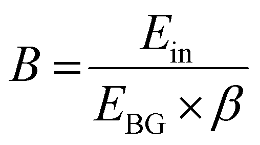 | (2) |
000 carriers per MeV photon in CsI:Tl.45 Carriers are then transferred to emission centres where they can emit in step iii.
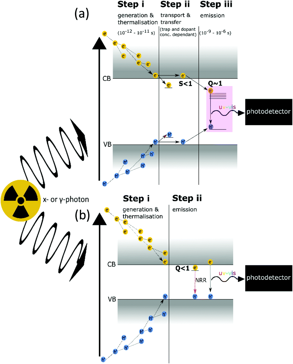 | ||
| Fig. 2 Schematic of the scintillation mechanism in extrinsic (a) and intrinsic (b) emitter systems (NRR = non-radiative recombination). The additional transfer step to the dopant energy levels (pink box) in extrinsic emitters increases the likelihood of charge carrier trapping causing losses and afterglow. | ||
A key mechanistic difference between different scintillator materials is the origin of the RL being intrinsic to the material, or the result of an extrinsic dopant. Extrinsic emitters, including CsI:Tl, GOS:Tb (Gd2O2S), and LYSO:Ce (Lu2(1-x)Y2xSiO5), are common commercially and the properties of extrinsic emission (Fig. 2a) depend on the activator ion.46 However, limitations of extrinsic materials arise in steps i and ii in the scintillation process. Firstly, to ensure efficient charge transfer in step ii, prevent thermal repopulation of emissive states, and reduce reabsorption of the scintillated light, the matrix band gap must be wider than the band gap of the dopant emission centre. The inverse relationship between the number of charge carriers generated in the cascade and the material band gap (eqn (2)) causes this wide gap host to limit the maximum number of generated emissive states. Secondly, carriers must diffuse to reach activation sites, increasing the time of scintillation and the probability of reaching a trap state. This leads to slow responses (for example 1 μs in CsI:Tl and 3 μs in GOS:Pr)47 and afterglow, while competing carrier trapping events can also quench carriers and reduce light yields. The efficiency of the energy migration phase, combined with the subsequent energy transfer to the activator site, is represented by the S term in eqn (1).
Intrinsic emission from direct band gap semiconductors, including PVKs and other emerging materials such as HgI2, PbI2 and II–VI semiconductors, occurs from band-to-band or excitonic states (Fig. 2b). Intrinsic emission allows narrower band gaps, increasing the maximum light yields. The absence of a transfer step in PVKs makes scintillation time scales limited by the emission step, and parity-allowed band-to-band or excitonic decay times can be less than nanoseconds. This makes PVKs potentially brighter and faster than traditional extrinsic materials; MAPbI3 materials can generate a theoretical maximum of ∼270000 charge carriers per MeV, over 4 times as many as CsI:Tl. Combined with the high atomic weights of key components, including lead (Z = 82), caesium (Z = 55) and iodine (Z = 53), this makes PVKs well suited to the application of indirect radiation detection.
2.2 Performance requirements
The broad uses of ionising radiation give an equally broad range of requirements for scintillators (see Table 1). An important parameter is the incident radiation energy, which dictates the scintillator thickness and influences the subsequent figures of merit displayed by a device (see Table S1, ESI†). It is also important to consider the indirect detection system as a combination of the scintillator with the photodetector and signal processing electronics. The emission from the scintillator must be detected by the photodetector, which requires efficient spectral overlap of the RL and the photodetector quantum efficiency, and appropriate optical coupling between the two devices.| Application | Energy range (keV) | Typical material | Current performance | Application specific requirements | ||
|---|---|---|---|---|---|---|
| Light yield (photons per MeV) | Decay time (ns) (afterglow) | Emission maximum (nm) | ||||
| Radiography (Medical) | 60–120 | CsI:Tl | 60000 [55] |
1000 (0.5% at 3 ms) [55] | 550 | • Spatial resolution |
| • Linear response with dose | ||||||
| Radiography (Industrial screening (food)) | 10–120 | GOS:Tb | 60000 [56] |
600000 (<0.1% at 3 ms) [57] |
545 | • Scalable to large dimensions to image large objects |
| • Emission wavelength suitable to silicon imagers | ||||||
| • Low cost | ||||||
| Computed tomography (Medical) | 80–140 | CdWO4 | 20000 [58] |
2000 (0.05% at 3 ms) [59] | 495 | • Temperature coefficient < 0.1% °C−1 from beam induced heating |
| • Afterglow < 0.1% at 3 ms | ||||||
| • Decay times below 10 μs to excced sampling rates | ||||||
| • Light yields > 20000 photons MeV−1 for good signal to noise |
||||||
| Mammography (Medical) | 20–40 | a-Se (direct detection) | n/a | n/a | n/a | • Spatial resolution ∼100 s μm (to detect low contrast tumours and microcalcifications) |
| Positron emission tomography (Medical) | 511 | LSO:Ce | 40000 [60] |
40 [60] | 420 | • Spatial resolution to accurately |
| • Determine line of response | ||||||
| • Energy resolution to reject scattered events | ||||||
| • Short emission decay times to reduce coincidence gate | ||||||
| TOF-positron emission tomography (Medical) | 511 | LaBr3:Ce | 61000 [61] |
35 [61] | 358 | • Timing resolution of 10 ps |
| Astronomy | 3–79 (NuSTAR) | CdZnTe (direct detection) | n/a | n/a | n/a | • Energy resolution of ∼1.5% at 60 keV |
| Calorimetry (High-energy physics) | Photons and electrons | Many: PbWO4 (LHC calorimetry) | 140 [62] | Several components: <10 ns, 20–200 ns, >500 ns [62] | 475 | • Energy resolution |
| • Large area fabrication 2 × 2 × 20 cm | ||||||
| • Sensitive to high energy photons | ||||||
| Gamma spectroscopy (Nuclear security) | 10–10000 |
NaI:Tl | 43000 [63] |
230 [64] | 415 | • Energy resolution to resolve isotopes <7% 662 keV |
| • Low cost for large areas | ||||||
Two essential attributes of a scintillator are bright and fast emission. The emission from a scintillator is quantified by its light yield, i.e., the number of photons emitted per MeV of incident radiation. Widespread commercial materials CsI:Tl and GOS:Tb both have light yields exceeding 60000 photons MeV−1,48 allowing sensitive detection. Fast emission is a requirement in many applications, particularly imaging with a high frame rate (CT) and to achieve high timing resolution (TOF-PET). Currently, fast emission is offered by the 5d–4f transition in lanthanides (Ce3+, Pr3+, Eu2+),49,50 which offer decay times on the nanosecond scale whilst maintaining high emission yields, for example LSO:Ce (Lu2SiO5), LYSO:Ce and LaBr3:Ce (Table 2). While the exact requirements differ between applications, scintillators must also be radiation-hard to withstand high-energy photon exposure, and be able to tolerate any environmental and mechanical stress that is required under operation. The high energy of the incident radiation is known to damage existing scintillators, generating defects which promote non-radiative losses and increase afterglow, as well as colour-centres that increase parasitic absorption.41 CsI:Tl based flat panel imagers are expected to lose sensitivity with repeated radiation exposure, and are warrantied up to 8730 Gy with <100 kV X-rays.51 Many existing scintillators are also hygroscopic (for example CsI:Tl/Na, NaI:Tl and LaBr3:Ce) which requires additional packaging and storage considerations.
| Material | Decay time (ns) | Ref. |
|---|---|---|
| a Low light yields from fast crossover component and slow excitonic emission limit commercial use. b μs background emission component also seen below 70 K that would contribute to afterglow. c Measured with UV excitation. It has been reported that the decay time measured from RL excitation is slower, due to the additional excitation and cascade steps.79 | ||
| CsI:Tl | 1000 | 55 |
| LSO:Ce | 40 | 60 |
| LYSO:Ce | 33 | 83 |
| LaBr3-Ce | 15 | 61 |
| LuI3-Ce | 31/140/1000 | 84 |
| LuAP:Ce | 17 | 85 |
| BGO | 300 | 86 |
| BaF2a | 0.8/630 | 87 |
| CsPbBr3 NCs | 44.6 | 38 |
| CsPbBr3 (7 K) | 1 (Fast component)b | 82 |
| MAPbBr3 (77 K) | 0.1/1 | 37 |
| PhePbBr4 | 9.4 | 66, 80 and 81 |
| 9.9 | ||
| 11 (81%)/36 (18%)/236 (1%) | ||
| CsPbBr3:Cs4PbBr6 | 3c | 73 and 74 |
| 1.4 (88%)/6.7 (12%) | ||
The use of ionising radiation to generate images is a key application of detectors, requiring high spatial resolution, linear response with incident intensity and low levels of afterglow. In general, the spatial resolution of indirect detectors has a lower fundamental limit than direct detectors due to light scattering in the scintillation step. To mitigate these losses, CsI:Tl can be evaporated into large needle like structures that aid waveguiding and improve spatial resolution. Such detectors typically use a Fibre Optic Plate (FOP) as a supporting structure, which has the added advantage of attenuating the primary X-ray beam, providing protection for the optical sensor. In addition, high light yields (∼60000 photons MeV−1) and mature fabrication techniques make CsI:Tl common in flat-panel imagers for medical radiography. Linear responses to incident intensity allow intensity discrimination between slight tissue density differences and such responses are primarily implemented by computed tomography, which has the benefit of consolidating large image sets, thereby reducing noise. Finally, a key requirement for imaging is low afterglow levels, which can distort image quality and reduce the modulation transfer function (MTF), especially in high frame-rate applications. Afterglow in CsI:Tl is high,52 limiting its use to longer integration times, with >2% emission remaining at 3 ms.53 Gamma-ray spectroscopy, security applications and high-energy physics all require the resolution of individual photon energies. Generating spectroscopic information requires operation of the detector in photon counting mode. The response of the scintillator must be proportional to the incident photon energy, and each photon must be analysed before the next one arrives, necessitating scintillator detectors with fast emission and fast processing electronics. The resolving ability of a scintillator is quantified by its energy resolution and an ideal indirect detector can resolve closely spaced gamma photons, such as the 604 and 662 keV emission of Cs isotopes.46 This requirement is particularly important in security applications and is fulfilled by NaI:Tl, with energy resolution around 7%54 (see ESI† for Definition) as well as a large light output of 43000 photons per MeV, and the ability to be fabricated in large dimensions.
3. PVK scintillator performance
3.1 Stopping power
PVKs have high mass attenuation coefficients due to their high-Z components. As a result, at 100 keV, a relevant energy for many imaging applications, the coefficient for MAPbI3 is 3.1 cm2 g−1, in comparison to 2.0 cm2 g−1 for CsI:Tl (Fig. 3a). However, the stopping power of a scintillator depends on the mass density of the material, not just the mass attenuation coefficient. The attenuation of photons through a solid can be obtained using the Beer–Lambert law (eqn (3)) which shows the dependence of the intensity of transmitted photons I on the material density ρ | (3) |
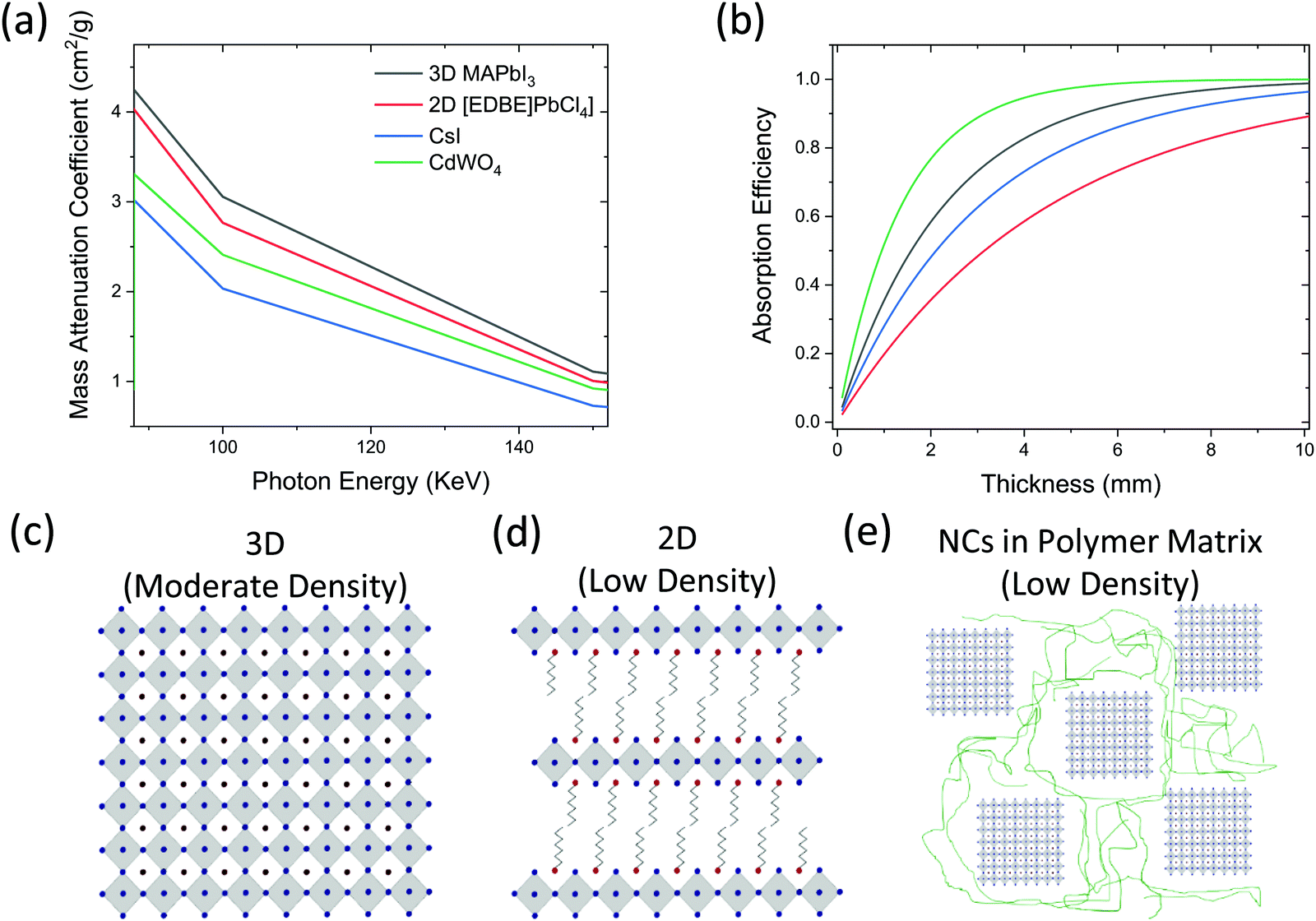 | ||
| Fig. 3 (a) Mass attenuation coefficient variation with photon energies relevant to medical imaging for PVK scintillators and commercial CsI and BGO materials (calculated in ref. 65) and (b) the corresponding absorption efficiency once material density is accounted for at 150 keV. The low efficiency of 2D PVKs to attenuate the incident photons highlights the requirement of high density materials (note legend is common in (a) and (b)). (c–e) Crystal Structure schematics demonstrating the detrimental effect of reducing dimensionality on material density by introducing low z organic components as a-site cations (d) or embedding nanocrystals in a polymer matrix (e). | ||
3.2 Light yields
Reports of room temperature light yields in PVKs have thus far been limited to reduced dimensionality systems, either through compositional or physical confinement, and this is proposed to be due to the increase in exciton binding energy preventing thermal quenching of the emissive states at room temperature (Fig. 4a). 2D PVKs (C6H5(CH2)2NH3)2PbBr4 ((Phe)PbBr4) and (EDBE)PbCl4 have displayed light yields of 1000066 and 900052 photons MeV−1, respectively. Similarly, all-inorganic CsPbBr3 systems have displayed RL, with nanocrystals (NCs) showing 5× higher emission intensity than YAlO3:Ce systems,38 and nanosheets67 yielding 21000 photons MeV−1. In contrast, bulk 3D systems such as MAPbBr3 single crystals, whose growth into large area thick layers is already well documented,68 have yet to display any appreciable scintillation at room temperature,36 with bulk CsPbBr3 emission intensities around 4 orders of magnitudes lower than CsPbBr3 NCs under the same conditions.38 The greater exciton binding energy of the NCs (up to 120 meV) compared to bulk PVK systems (<15 meV69) was reasoned to prevent thermal quenching of the emissive state. A strong temperature dependence of light yield has been found in PVK materials70 (Fig. 4b), allowing bright emission even from 3D systems at low temperatures.52 Light yields of 90000 ± 18000 and 116000 ± 23000 photons MeV−1 at 77 K and 8 K respectively have been demonstrated in MAPbBr3 single crystals,37 consistent with a freezing out of the thermal dissociation of excitons, which when combined with the low trap densities (∼1010 cm−3)71 promotes efficient radiative recombination.
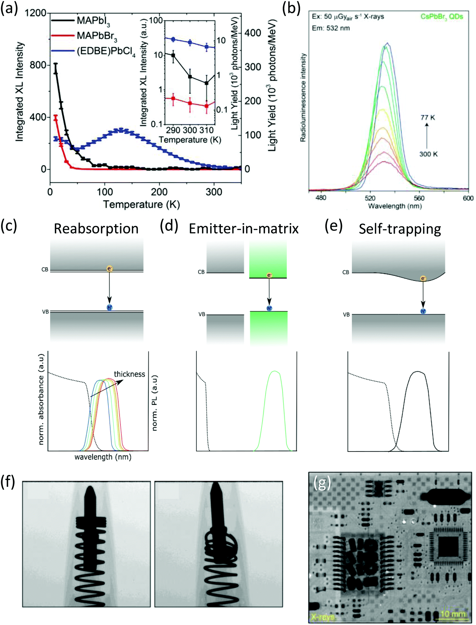 | ||
| Fig. 4 (a) Temperature and dimensionality dependence of PVK RL from 3D MAPbX3 single crystals, and 2D (EDBE)PbCl4, showing higher room temperature emission from the reduced dimensionality system. Reproduced from ref. 52 with permission from Springer Nature. (b) Temperature dependence of CsPbBr3 NC RL. Reprinted with permission from Springer Nature.38 (c–e) Schematics of energy levels and expected absorption (dashed lines) and emission spectra (solid lines), highlighting the self-absorption issue with PVKs and possible solutions. (c) Band-to-band emission with significant overlap between the absorption and emission spectra. The normalised emission as thickness increases shows the expected redshift due to reabsorption of the shorter wavelengths. (d) Reintroducing the extrinsic mechanism with an emitter-in-matrix system. (e) Self-trapped exciton emission with large Stokes shift. (f–g) Images taken with PVK scintillators (f) CsPbBr3 NCs imaging a ball point pen. Reproduced from ref. 39 with permission from Wiley. (g) CsPbBr3 NCs imaging a network interface card. Reprinted with permission from Springer Nature.38 | ||
While promising, the room temperature light yields of PVKs are suggestive of losses, and parasitic self-absorption of the emitted photons will limit external emission of the photons (i.e., RL intensities). For example, the intrinsic emission spectrum of direct band gap semiconductors with small Stokes shifts, such as 3D PVKs, overlaps with their absorption spectra, and this causes significant reabsorption and thus limits light yields (Fig. 4c). Self-absorption in thick PVK materials was originally studied under optical excitation, where Wenger et al.72 found that increasing thickness decreases the intensity and redshifts the photoluminescence emission through reabsorption particularly of the higher energy photons. The external photoluminescence quantum efficiency (PLQE) of 2 mm-thick MAPbBr3 crystals was reported to be 6.4% despite internal values calculated to be 67%, and reducing this disparity has since become a focus in the scintillator community.
Solutions to reduce the impact of reabsorption have exploited the embedding of the PVK emitter within a wide band gap matrix (Fig. 4d). This includes CsPbBr3 NCs contained in a wide band gap Cs4PbBr6 matrix, where the matrix contributes to the stopping power and helps stabilise the emission centres.73 The strong confinement in the 0D structure yields an exciton binding energy of ∼90 meV and, combined with reduced self-absorption, led to light yields of 64000 photons MeV−1 at room temperature.74 Similarly, an organic dye with a large Stokes shift has been combined with CsPbBr3 NCs, where efficient sensitisation by the PVK and emission by the organic component at longer wavelengths75 minimises reabsorption losses. However, the final device offered only moderate RL intensity, comparable to BGO (8200 photons MeV−1). A similar system was proposed by Ning et al.76 for visible light conversion, where PbS quantum dots were fabricated within a perovskite, with the NIR emission from the quantum dots shifted well away from the PVK absorption onset, minimising reabsorption. Localisation and relaxation of emissive species with the lattice can induce a Stokes shift, and negligible self-absorption was demonstrated in 1D structured Rb2CuBr3 due to self-trapping of excitons77 (Fig. 4e). The exceptional PLQE values of 98.6% translated to approximate light yields of 91000 photons MeV−1, the highest room temperature value from PVK scintillators to date. Emission from self-trapped excitons was also seen in the Cs2Ag0.6Na0.4In1−yBiyCl6 double perovskite,78 where the Bi3+ doping can be used to tune the radiation stopping power due to its high atomic number. An optimum of 15% loading produced light yields of ∼39000 photons per meV. However, these self-trapped excitonic systems are prone to longer decay times on the order of tens of microseconds, with considerable afterglow in Rb2CuBr3 of 2.72% at 20 ms, and thus may be more suitable for a more limited range of applications.
3.3 Response speeds
PVK scintillation has been shown to occur very rapidly, with fast decay times presented in literature. CsPbBr3 nanocrystal scintillators demonstrated a short decay time of 44.6 ns under gamma excitation.38 The same material displayed a 5 ns decay time upon UV excitation, with the faster decay potentially due to avoiding the additional excitation and cascade steps in RL,79 combined with the shorter penetration depth of UV compared to X-rays exciting the surface. The decay time shortened to 3 ns once combined in a Cs4PbBr6 matrix, attributed to additional confinement accelerating recombination.73 A similar CsPbBr3:Cs4PbBr6 system has recently offered impressively short RL decays, with a 1.4/6.7 ns fast and slow component, showing promise for fast detection applications.74 2D perovskites have displayed rapid room temperature decay times, with (EDBE)PbCl4 demonstrating a single decay component of 7.9 ns from UV-Vis excitation,52 and (Phe)PbBr4 has been measured independently to have a dominant decay time of around 10 ns,80,81 offering considerable improvement on current materials (Table 2). Studying the scintillation temperature dependence from MAPbBr3 single crystals, Mykhaylyk et al.37 demonstrated that above 60 K the emission components retain impressive decay times of 0.1/1 ns respectively, which combined with increased light yields of ∼90000 photons MeV−1 at liquid nitrogen temperature make this a prospect for ultrafast timing precision. Similarly, RL from CsPbBr3 single crystals reached 1 ns at 7 K, and outperformed LYSO:Ce at resolving a pulsed synchrotron beam.82 Detector cooling is already a feature in HP–Ge direct detectors, operated at 77 K due to the small material band gap, and so is a commercial possibility for PVKs.
3.4 Stability
The tolerance of PVK scintillators to X- and gamma-rays has not been studied in detail, though initial results look promising. Reports have demonstrated steady RL intensity under continuous irradiation for several hours in CsPbBr3 NCs38 and nanosheets (2 hours at 18 μGy s−1).88 Higher doses have also been tolerated by PVK scintillators, with Cs2Ag0.6Na0.4In0.85Bi0.15Cl6 showing negligible losses after 50 hours and a 34 Gy cumulative dose,78 whereas 800 Gy reduced the RL intensity of CsPbBr3 NCs with an organic dye to just 85% of its initial value.75 Although reductions in light output begin to show at these doses74 – tridoped Cs2Ag0.6Na0.4InCl6:Yb3+/Er3+/Bi3+ reduced its RL to 49% after 53 Gy89 – they still outperform traditional materials, as CsI:Tl emission dropped to 28% after the same dose. An improved understanding of the degradation mechanisms from more focussed studies correlating the effect of the high-energy radiation on both the PVK material and the scintillation performance would benefit the field enormously. The stability of PVKs in direct detectors may also provide useful understanding in this context. A perovskite-in-polymer membrane system showed negligible current reduction after a total dose of 376.8 Gy (equivalent to 1.88 million chest X-rays)90 while MAPbBr3 single crystals irradiated with a 230 Gy dose over 10 hours displayed no losses.91 The retention of charge transport properties would suggest no significant material degradation, which is promising for scintillators.There are also studies on the effect of high-energy radiation on PVK solar cells. The importance of efficiency, weight and size have made PVKs a promising prospect for space applications, and as such there is are efforts to analyse the tolerance of these materials to radiation. Gamma-ray studies have shown small losses in Jsc in mixed-halide systems, due to radiation-induced phase segregation,92 similar to the Hoke effect,93 although the largest losses are due to colour centers in the glass reducing transmittance.94 The broad quantum efficiency of most photodetectors used in combination with scintillators makes precise tuning of the band gap by alloying different halides less important than in solar cells; as a result this phase segregation should not impact PVK indirect detectors. A range of PVK absorbers were tested by Boldyreva et al.,95 with MAPbI3 displaying remarkable stability after 1 MRad (equivalent to 10 kGy) of gamma exposure, attributed to CH3I and NH3 undergoing radiation-induced radical chemistry that then self-heal any generated defects. Similarly, MAPbI3 was tested in an energy converter application, and devices showed no performance degradation after a 57 Gy gamma dose (57 Sv H*(10)).96 The radiation hardness of PVKs has also been shown to extend to protons and electrons, demonstrating a similar self-healing behaviour after irradiation.97,98 It is proposed that the lability of the constituent ions in PVK structures allows any defects formed by the radiation to be removed, limiting and recovering from, any damage. In addition, many defects in PVKs introduce only shallow states, and so radiation-induced defects may be benign to operation.99 The moisture instability of PVKs may require encapsulation in end designs, which may further complicate outcoupling considerations. However, many current materials suffer from hygroscopicity100 and detector designs often guard against this.
3.5 Full device performance
Despite a short period of development, PVK scintillators have already been incorporated in full indirect detection systems, displaying impressive performance. High MTF values have been reported in NC-based PVK imagers, which exhibit reduced internal light scattering compared to bulk films and single crystals. The resulting reduction in optical crosstalk is promising for high-resolution imaging applications. MTF values of 9.81 lpmm−1 (MTF = 0.2)39 and MTF = 0.72 at 2 lpmm−138 have been reported in CsPbBr3 NCs, exceeding the performance of GOS and CsI:Tl reference devices, respectively. Examples of images produced with PVK scintillators are shown in Fig. 4f–g. The short decay times of the Cs2Ag0.6Na0.4In1−yBiyCl6 double perovskite enabled a dynamic image of a bending finger to be produced, possible at low incident doses of 47.2 μGys−1.78 However, initial resolution of 4.3 lpmm−1 (MTF = 0.2) dropped to 1.4 lpmm−1 as wafer thickness increased from 0.1 to 0.6 mm due to increased light scattering within the scintillator. Linear responses between 30 – 550 μGys−1, the limits of the X-ray source utilised in the study,77 have been presented, as well as linearity down to 13 nGys−1, an encouraging result for low dose imaging.38 Apart from self-trapped PVK emission, reports on PVKs have displayed virtually no afterglow (5 ppm at 20 ms81), offering levels similar to commercial BGO and CdWO4. Combined with the short decay times, this may open up use in even faster frame rates than is currently possible.
There have also been reports of energy resolution from PVK spectroscopic systems. For example, (Phe)PbBr4 crystals exhibited an energy resolution of 35 ± 5% (662 keV) with a linear response over the 122–662 keV range,81 and a similar lithium doped (PEA)2PbBr4 (PEA = phenethylammonium) system presented 12.4% (662 keV).101 In addition, MAPbBr0.05Cl2.95 demonstrated an improved 10.5 ± 0.4% (662 keV).102 A CsPbBr3:Cs4PbBr6 powder presented the best energy resolution values in PVKs to date of 3.0 ± 0.1% (59.6 keV) which shows promise in this application.74 Overall, although current performance falls short of specific energy resolving detectors, such as Silicon Drift Detectors (SDDs), the energy resolution of PVKs is largely unexplored and represents an exciting area for further development.
4. Outlook
PVKs have thus far shown enormous promise as scintillating materials, demonstrating good light yields and impressively short decay times, all from low temperature solution synthesis. However, there remains plenty of room for improvement in their performance metrics to reach their potential, while selecting the applications where PVKs can have the most impact requires consideration.4.1 Improving scintillator light yields: learning lessons from PVK photovoltaics and LEDs
The large cascade of charge carrier generation gives PVK scintillators high theoretical light yields, but to date recorded values are much lower. Common themes emerge to explain these losses: competing non-radiative recombination processes lowering internal light yields, and outcoupling issues, due to reabsorption preventing efficient light escape. Solutions to these challenges could be found within the field of PVKs for solar cells and LEDs where maximising radiative efficiency and optoelectronic performance is paramount.Removing trap states via passivation is common in PVK thin films to overcome the high defect densities,106,107 with a wide range of methods shown to raise emission efficiencies, demonstrating internal PLQEs exceeding 95%.108 Successful approaches include adding passivating agents to the precursor solution,108,109 chemical post treatment110,111 and light soaking,112,113 with species such as phosphate based molecules binding to uncoordinated lead sites,114 2D molecules forming well passivated quasi-2D perovskite surfaces,115 or alkali halides binding excess halide species.108 In thin-film devices, the short penetration depth of UV-Vis light and the importance of any interfaces with charge transport layers makes surface defects highly important, and often the target of passivation techniques. However, the increased thickness and deeper charge carrier generation in scintillators makes bulk trap states more relevant and passivation techniques targeting these bulk traps would be important. Systematic passivation approaches to PVK scintillators are yet to be reported.
Raising PLQEs by increasing the charge carrier density into the bimolecular regime is another prevalent tactic in solar cells and LEDs. Reducing the material volume in LEDs by decreasing PVK thickness can allow charge carrier densities to exceed trap-assisted recombination levels,116 but the necessity of thick materials to be sufficiently attenuating makes this approach impractical for scintillators. An alternative method to increase carrier densities involves the use of charge carrier funnelling to enhance radiative efficiency. Quasi-2D materials, with n (n > 1) layers of PbI6 octahedra between large organic spacers contain a mixture of n layered phases, with carrier funnelling to the lowest band gap occurring. PLQEs above 10% at low excitation fluences of 6 mW cm−2 resulted from the high carrier concentrations (∼1016 cm−3) within these low band gap phases, translating into efficient LED devices.117 The lower energy emission from the smallest band gap would also contribute to reduced reabsorption. However, the compositional engineering of these phases is complex, and can introduce additional defects and grain boundaries that limit radiative efficiency, and require additional passivation.114 This may add complications when scaling up to the large volume of material needed in radiation detection. A solution may come from the finding that mixed halide PVKs can self-organise into band gap gradients, an effect that can be stabilised by cation selection, to achieve similar charge carrier concentration but with greater potential for upscaling;118 more work is needed to control such gradients and implement into scintillators.
While photon recycling allows additional attempts at emission, better outcoupling increases the probability of emitted photons escaping the scintillator and reaching the photodetector. This is achievable using photonic structures, which have recently emerged as a concept to improve the performance of existing high refractive index scintillators.123–126 Increasing the cone of emission will improve light yields of scintillators, with simulations suggesting 90–110% enhancements,124 and increase the timing resolution, by increasing the likelihood that light is emitted at the first instance it meets the scintillator/detector interface, increasing the light yield at early times.123 Spatial resolution would also improve through decreased lateral distances between the point of emission and detection by the photodetector. Better optical coupling between the scintillator and detector can provide similar performance improvements, possible in PVK devices by direct deposition onto photodetectors (discussed in Section 4.2.2) or on to fibre-optic plate structures. These performance benefits are of relevance to PVK scintillators yet such approaches remain unexplored. There have been examples of photonic structures improving the performance of PVK lasers127,128 and also coloured solar cells.129 Extending this to scintillators would be a fruitful prospect, and could prove simpler due to the absence of any additional transport layers on the surface.
4.2 Applications and opportunities
Besides the exceptional emission properties, PVK materials also have unique features, such as band gap tunability and solution processibility, which provide further advantages over existing materials and potential opportunities for novel detector applications.Low temperature deposition also enables compatibility with flexible substrates, resulting in a detector that can conform to surfaces, useful in medical diagnostics and non-destructive testing.138 The importance of flexible radiation detectors was well explained by Zhao et al.,90 whereby intensity differences between pixels in the centres and edges of the detector from point X-ray sources can result in imaging errors and misdiagnosis139 (Fig. 5a). Substrate flexibility also allows better non-destructive industrial imaging by being placed inside of objects and thus requiring softer beam energies and thinner scintillators (Fig. 5b). Flexible PVK devices are well developed,140 with flexible solar cells exceeding 19% power conversion efficiency,141 and flexible direct X-ray detectors demonstrated.142–144 Retaining flexibility with increasing PVK thickness is a challenge, and a PVK in a porous nylon membrane, developed for flexible direct X-ray detection, demonstrated 2/3 mm minimum bending radii in 130/240 μm thick devices, respectively. However, unlike direct detectors and solar cells, which require charge transport considerations and compatible transport layers and contacts,145 scintillators are much simpler, making the prospect of developing a flexible scintillator promising. Alternate uses of flexibility could include accurately measuring dose delivery with detectors conforming to body parts. Despite lead-based PVK scintillators being exempt from EU regulations on hazardous substances in electronic equipment (RoHS),146 applications requiring closer contact with the human body may require less toxic analogues. Alternative metals such as copper, europium, bismuth and tin have all been integrated into perovskite-like structures and demonstrated scintillation.78,147–152 Lead-free indirect detectors have demonstrated exceptional performance, and currently present the highest light yields of PVK materials to date (Rb2CuBr3 ∼ 91000 photons per MeV,147 Cs4EuX6 ∼ 78000 photos per MeV151). However, the decrease in stopping power when replacing lead with a lower atomic number element must be considered.
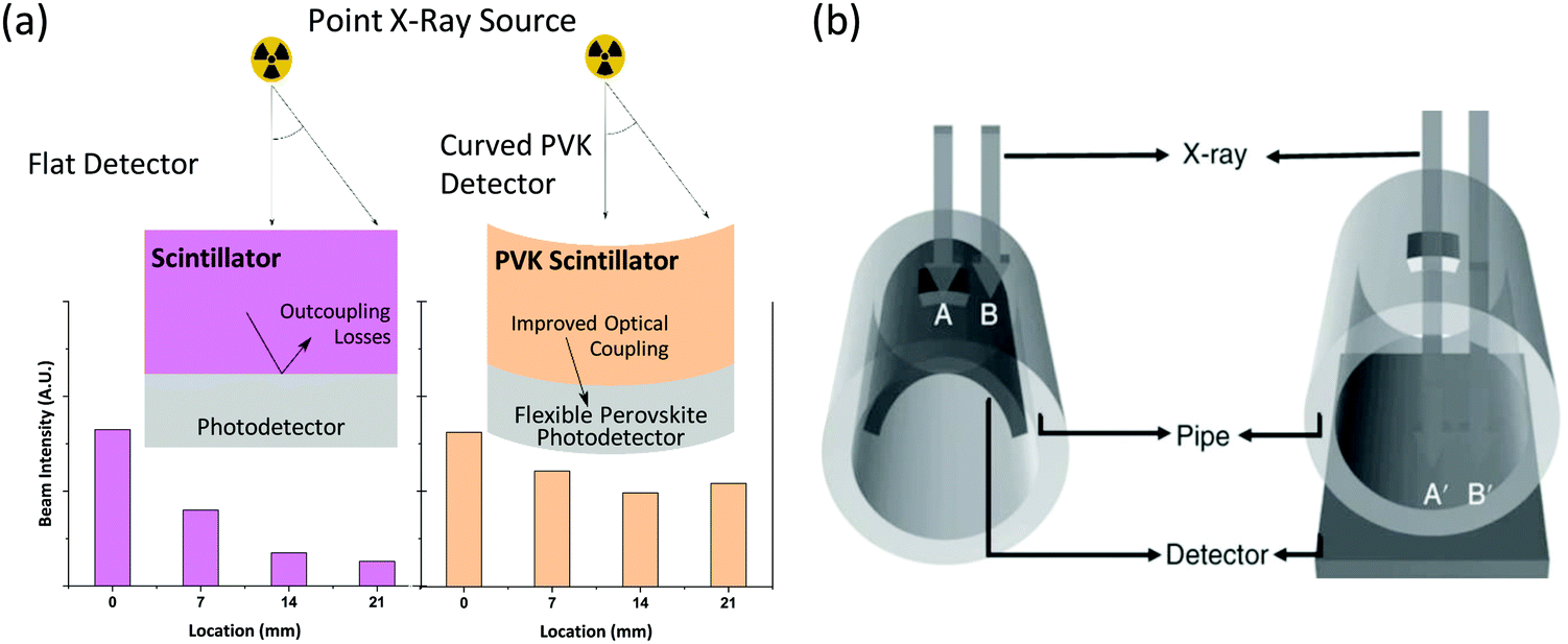 | ||
| Fig. 5 Potential for unique functionality with flexible PVK scintillators. (a) Overcoming uneven X-ray intensity distributions from point sources with flexible PVK scintillators and photodetectors. Scintillators can be combined with flexible PVK photodetectors, which can simplify fabrication of the full indirect detector system and potentially improve light outcoupling from scintillator to photodetector. Adapted by permission from Springer Nature.90 (b) Flexible detectors conforming to the inside of a pipe allow lower energy radiation and consequently thinner scintillators with enhanced spatial resolution. Reprinted with permission from Springer Nature.90 | ||
There are significant cost reductions in the material production of PVKs compared to commercial scintillator materials, as cheap and earth-abundant precursor materials, combined with low temperature (<150 °C) and ambient processing conditions, contribute to inexpensive production. An analysis was presented by Cao et al.73 in their growth of CsPbBr3:Cs4PbBr6, suggesting the cost of a crude ingot was similar to CsI:Tl, while considerable savings up to a factor of 2000% can be made over Ce3+ doped materials (LYSO, YAG, YAP used for spectroscopic applications) without the concerns on the supply and extraction of rare-earth materials.153 High-throughput production of PVKs have also been projected to bring costs down further in other areas, for example in photovoltaics,154 where scalable techniques, such as slot-die coating,155 doctor blading,24 inkjet printing156 and thermal evaporation157 have all been demonstrated. It was estimated that detectors for CT, PET, SPECT (single-photon emission computed tomography) and high energy physics require over 70000 kg of scintillator material annually at today's usage alone,158 emphasising the importance on the scalability of production.
162–164 suiting high sensitivity requirements. Flexible PVK photodetector arrays have already been demonstrated,165 highlighting the potential for an all-perovskite system to offer functionality beyond that of current materials, specifically for PET detectors. From a commercial perspective, these devices would also simplify detector fabrication, and could overcome outcoupling problems with refractive index matching to reduce internally reflected RL. Self-powered photodetectors166–168 would enable greater portability, by avoiding the need for bulky power supplies, improving access to radiation detector systems. This is relevant in healthcare, where patients may not have access to hospitals, as well as industrial radiography and mobile security, in conjunction with small and portable radionuclide gamma sources.
000 photons per ns, are required.171 This has already shown to be possible in cooled perovskite single crystals,37 which may enable deployment in this role (Fig. 6b and c). Additional work towards fast, room temperature emitters will be further enabling.
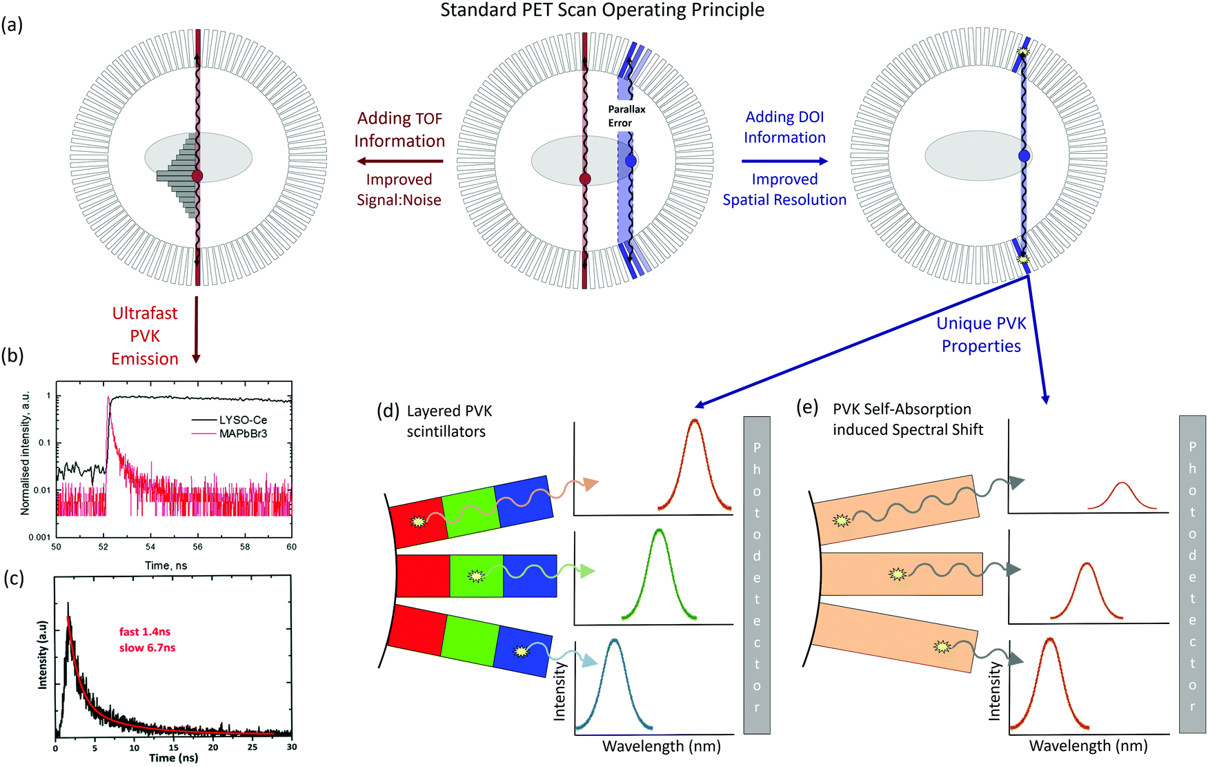 | ||
| Fig. 6 (a) The operating principle and existing issues of PET (centre) with parallax errors from off-centre detector line of response (LOR). Adding TOF information (left) provides information of the interaction position along the LOR, and depth information (right) increases spatial resolution. (b and c) Demonstrations of ultrafast PVK scintillation to provide TOF information. Reproduced from ref. 37 and 74, respectively, with permission from The Royal Society of Chemistry. (d and e) Utilising PVK to add depth information by (d) layering different band gap materials and (e) exploiting the spectral change from RL self-absorption. | ||
PVK based detectors can also improve the spatial resolution of PET scanners by adding depth of interaction (DOI) information. The penetration of 511 keV photons requires long scintillator crystals which limits the spatial resolution, and causes parallax errors from off-centre photons not approaching the scintillator perpendicularly.172 This is particularly problematic in small ring systems. Adding depth information is possible with the wide range of PVK scintillator materials, with layers of two or more detector materials with different decay times or emission wavelengths, which can be distinguished by the photodetector (Fig. 6d). Alternatively, it could be possible to use the self-absorption of PVKs and the associated spectral change to determine the depth of interaction. With an accurate understanding of the optical properties of the crystal, the increased red shifting as a function of interaction depth would demonstrate the position of absorption, combined with a hyperspectral camera (Fig. 6e). Overall, there is a range of possibilities for the unique properties of PVKs to improve current PET systems, demonstrating the commercial potential of the material.
5. Conclusion
Owing to their intrinsic scintillation, combined with novel material properties, PVKs have the potential to increase the functionality of indirect detectors beyond current possibilities. The reported exceptional light yields and fast emission decay times holds promise for many applications, especially TOF systems, while the unique features of PVK materials expands the range of systems in which they can be utilised, from flexible systems to multispectral layered detectors. Furthermore, a low cost and simple fabrication may enable cost savings over existing materials, with the considerable simultaneous research on these materials for other optoelectronic applications relaxing the expected strain of upscaling to commercial levels. Despite admirable progress in a short time, there remains enormous room to develop these materials, primarily by reducing the disparity between experimental and maximum theoretical light yields, and the lack of application-specific degradation studies. Engineering materials with greater Stokes shifts, lower trap densities and/or with control of carrier density and recombination sites will bring improvements in photon outcoupling and luminescence yields; indeed, further advances in other PVK light emitting applications will feed back to further improve their scintillator applications. The promising radiation hardness and even self-healing already demonstrated in preliminary studies, combined with the carefully controlled end-use environments, means the use of halide perovskites as scintillator detectors will not be far from commercial application.Conflicts of interest
There are no conflicts to declare.Acknowledgements
This project has received funding from the European Research Council (ERC) under the European Union's Horizon 2020 research and innovation programme (HYPERION, grant agreement number 756962 and PEROVSCI, grant agreement number 957513). ODIM acknowledges funding from a departmental awarded EPSRC Doctoral Training Studentship. MA acknowledges funding from the European Union's Horizon 2020 research and innovation programme under the Marie Skłodowska-Curie grant agreement No. 841386. TASD acknowledges a National University of Ireland Travelling Studentship. SDS acknowledges support from the Royal Society and Tata Group (UF150033).References
- G. F. Knoll, Radiation Detection and Measurement, Wiley, New York, 4th edn, 2010 Search PubMed.
- M. Spahn, Nucl. Instrum. Methods Phys. Res., Sect. A, 2013, 731, 57–63 Search PubMed.
- S. K. Mathanker, P. R. Weckler and N. Wang, Trans. ASABE, 2013, 56, 1213–1226 Search PubMed.
- H. E. Martz, C. M. Logan, D. J. Schneberk and P. J. Shull, X-Ray Imaging: Fundamentals, Industrial Techniques and Applications, CRC Press, Boca Raton, FL, 1st edn, 2017 Search PubMed.
- R. Hanke, T. Fuchs and N. Uhlmann, Nucl. Instrum. Methods Phys. Res., Sect. A, 2008, 591, 14–18 Search PubMed.
- B. K. Agarwal, X-Ray Spectroscopy: An Introduction, Springer, Berlin Heidelberg, New York, 2nd edn, 1991 Search PubMed.
- M. Güdel and Y. Nazé, Astron. Astrophys. Rev., 2009, 17, 309–408 Search PubMed.
- A. S. K. Arnaud and R. Smith, Handbook of X-ray Astronomy, Cambridge University Press, Cambridge, 1st edn, 2011 Search PubMed.
- J. Glodo, Y. Wang, R. Shawgo, C. Brecher, R. H. Hawrami, J. Tower and K. S. Shah, Phys. Procedia, 2017, 90, 285–290 Search PubMed.
- S. N. Ahmed, Physics and Engineering of Radiation Detection, Academic Press, San Diego, 1st edn, 2007 Search PubMed.
- G. Lutz, Semiconductor Radiation Detectors, Device Physics, Springer Berlin, Heidelberg, Berlin, 1st edn, 2007 Search PubMed.
- N. Rao, B. Ament, R. Parmee, J. Cameron and M. Mayo, J. Pharm. Innovation, 2018, 13, 270–282 Search PubMed.
- P. Lecoq, IEEE Trans. Nucl. Sci., 2012, 59, 2313–2318 Search PubMed.
- P. A. Rodnyi, Radiat. Meas., 2001, 33, 605–614 Search PubMed.
- S. E. Derenzo, E. Bourret-Courshesne, G. Bizarri and A. Canning, Nucl. Instrum. Methods Phys. Res., Sect. A, 2016, 805, 36–40 Search PubMed.
- International Agency for Research on Cancer IARC, A Review of Human Carcinogens. Part D: Radiation, Lyon, 2009.
- Sheila Dixon, Diagnostic Imaging Dataset Annual Statistical, 2017.
- Public Health England Patient dose information: guidance, https://www.gov.uk/government/publications/medical-radiation-patient-doses/patient-dose-information-guidance, accessed May 2020.
- Best Research-Cell Efficiency Chart | Photovoltaic Research | NREL, https://www.nrel.gov/pv/cell-efficiency.html, accessed 25 June 2020.
- K. Frohna and S. D. Stranks, in Handbook of Organic Materials for Electronic and Photonic Devices, ed. O. Ostroverkhova, Woodhead Publishing, Cambridge, 2nd edn, 2019, ch. 7, pp. 211–256 Search PubMed.
- C. C. Stoumpos, C. D. Malliakas, J. A. Peters, Z. Liu, M. Sebastian, J. Im, T. C. Chasapis, A. C. Wibowo, D. Y. Chung, A. J. Freeman, B. W. Wessels and M. G. Kanatzidis, Cryst. Growth Des., 2013, 13, 2722–2727 Search PubMed.
- Q. Dong, Y. Fang, Y. Shao, P. Mulligan, J. Qiu, L. Cao and J. Huang, Science, 2015, 347, 967–971 Search PubMed.
- H. Wei, Y. Fang, P. Mulligan, W. Chuirazzi, H. H. Fang, C. Wang, B. R. Ecker, Y. Gao, M. A. Loi, L. Cao and J. Huang, Nat. Photonics, 2016, 10, 333–339 Search PubMed.
- Y. C. Kim, K. H. Kim, D. Y. Son, D. N. Jeong, J. Y. Seo, Y. S. Choi, I. T. Han, S. Y. Lee and N. G. Park, Nature, 2017, 550, 87–91 Search PubMed.
- S. Tie, W. Zhao, D. Xin, M. Zhang, J. Long, Q. Chen, X. Zheng, J. Zhu and W. H. Zhang, Adv. Mater., 2020, 32, 1–7 Search PubMed.
- X. Zheng, W. Zhao, P. Wang, H. Tan, M. I. Saidaminov, S. Tie, L. Chen, Y. Peng, J. Long and W. Zhang, J. Energy Chem., 2020, 49, 299–306 Search PubMed.
- W. Wei, Y. Zhang, Q. Xu, H. Wei, Y. Fang, Q. Wang, Y. Deng, T. Li, A. Gruverman, L. Cao and J. Huang, Nat. Photonics, 2017, 11, 315–321 Search PubMed.
- G. J. Matt, I. Levchuk, J. Knüttel, J. Dallmann, A. Osvet, M. Sytnyk, X. Tang, J. Elia, R. Hock, W. Heiss and C. J. Brabec, Adv. Mater. Interfaces, 2020, 7, 1901575 Search PubMed.
- Y. Huang, L. Qiao, Y. Jiang, T. He, R. Long, F. Yang, L. Wang, X. Lei, M. Yuan and J. Chen, Angew. Chem., Int. Ed., 2019, 58, 17834–17842 Search PubMed.
- B. Yang, W. Pan, H. Wu, G. Niu, J.-H. Yuan, K.-H. Xue, L. Yin, X. Du, X.-S. Miao, X. Yang, Q. Xie and J. Tang, Nat. Commun., 2019, 10, 1989 Search PubMed.
- B. Bin Zhang, X. Liu, B. Xiao, A. Ben Hafsia, K. Gao, Y. Xu, J. Zhou and Y. Chen, J. Phys. Chem. Lett., 2020, 11, 432–437 Search PubMed.
- H. Wei and J. Huang, Nat. Commun., 2019, 10, 1066 Search PubMed.
- A. N. Belsky, P. Chevallier, P. Dhez, P. Martin, C. Pédrini and A. N. Vasil’ev, Nucl. Instrum. Methods Phys. Res., Sect. A, 1995, 361, 384–387 Search PubMed.
- A. N. Belsky, P. Chevallier, E. N. Mel’chakov, C. Pédrini, P. A. Rodnyi and A. N. Vasil’ev, Chem. Phys. Lett., 1997, 278, 369–372 Search PubMed.
- K. Shibuya, M. Koshimizu, Y. Takeoka and K. Asai, Nucl. Instrum. Methods Phys. Res., Sect. B, 2002, 194, 207–212 Search PubMed.
- K. Shibuya, M. Koshimizu, K. Asai and H. Shibata, Appl. Phys. Lett., 2004, 84, 4370–4372 Search PubMed.
- V. B. Mykhaylyk, H. Kraus and M. Saliba, Mater. Horiz., 2019, 6, 1740–1747 Search PubMed.
- Q. Chen, J. Wu, X. Ou, B. Huang, J. Almutlaq, A. A. Zhumekenov, X. Guan, S. Han, L. Liang, Z. Yi, J. Li, X. Xie, Y. Wang, Y. Li, D. Fan, D. B. L. Teh, A. H. All, O. F. Mohammed, O. M. Bakr, T. Wu, M. Bettinelli, H. Yang, W. Huang and X. Liu, Nature, 2018, 561, 88–93 Search PubMed.
- J. H. Heo, D. H. Shin, J. K. Park, D. H. Kim, S. J. Lee and S. H. Im, Adv. Mater., 2018, 30, 1–6 Search PubMed.
- M. Sytnyk, S. Deumel, S. F. Tedde, G. J. Matt and W. Heiss, Appl. Phys. Lett., 2019, 115, 19051 Search PubMed.
- P. A. Rodnyi, Physical Processes in Inorganic Scintillators, CRC Press, Boca Raton, 1st edn, 1997 Search PubMed.
- C. A. Klein, J. Appl. Phys., 1968, 39, 2029–2038 Search PubMed.
- W. Van Roosbroeck, Phys. Rev., 1965, 139, 1702–1716 Search PubMed.
- A. Rothwarf, J. Appl. Phys., 1973, 44, 752–756 Search PubMed.
- P. A. Rodnyi, P. Dorenbos and C. W. E. van Eijk, Phys. Status Solidi, 1995, 187, 15–29 Search PubMed.
- T. Yanagida, Proc. Jpn. Acad., Ser. B, 2018, 94, 75–97 Search PubMed.
- F. Maddalena, L. Tjahjana, A. Xie, A. Arramel, S. Zeng, H. Wang, P. Coquet, W. Drozdowski, C. Dujardin, C. Dang and M. Birowosuto, Crystals, 2019, 9, 88–97 Search PubMed.
- C. W. E. van Eijk, Nucl. Instrum. Methods Phys. Res., Sect. A, 2003, 509, 17–25 Search PubMed.
- C. W. E. van Eijk, Nucl. Tracks Radiat. Meas., 1993, 21, 5–10 Search PubMed.
- C. W. E. van Eijk, Proc. SPIE-Int. Soc. Opt. Eng., 1996, 2706, 158–167 Search PubMed.
- Hamamatsu Flat panel sensor C7942CA-22 Data Sheet, https://www.hamamatsu.com/us/en/product/type/C7942CA-22/index.html, accessed September 2020.
- M. D. Birowosuto, D. Cortecchia, W. Drozdowski, K. Brylew, W. Lachmanski, A. Bruno and C. Soci, Sci. Rep., 2016, 6, 37254 Search PubMed.
- C. W. E. van Eijk, Phys. Med. Biol., 2002, 47, 85–106 Search PubMed.
- C. Celiktas, E. E. Ermis and M. Bayburt, J. Radioanal. Nucl. Chem., 2012, 293, 377–382 Search PubMed.
- J. D. Valentine, W. W. Moses, S. E. Derenzo, D. K. Wehe and G. F. Knoll, Nucl. Instrum. Methods Phys. Res., Sect. A, 1993, 325, 147–157 Search PubMed.
- C. M. Carpenter, C. Sun, G. Pratx, R. Rao and L. Xing, Med. Phys., 2010, 37, 4011–4018 Search PubMed.
- P. Lecoq, Nucl. Instrum. Methods Phys. Res., Sect. A, 2016, 809, 130–139 Search PubMed.
- C. Michail, V. Koukou, N. Martini, G. Saatsakis, N. Kalyvas, A. Bakas, I. Kandarakis, G. Fountos, G. Panayiotakis and I. Valais, Crystals, 2020, 10, 429 Search PubMed.
- V. B. Mikhailik and H. Kraus, J. Phys. Stud., 2010, 14, 4201 Search PubMed.
- C. L. Melcher and J. S. Schweitzer, IEEE Trans. Nucl. Sci., 1992, 39, 502–505 Search PubMed.
- E. V. D. Van Loef, P. Dorenbos, C. W. E. Van Eijk, K. W. Krämer and H. U. Güdel, Nucl. Instrum. Methods Phys. Res., Sect. A, 2002, 486, 254–258 Search PubMed.
- P. Lecoq, I. Dafinei, E. Auffray, M. Schneegans, M. V. Korzhik, O. V. Missevitch, V. B. Pavlenko, A. A. Fedorov, A. N. Annenkov, V. L. Kostylev and V. D. Ligun, Nucl. Instrum. Methods Phys. Res., Sect. A, 1995, 365, 291–298 Search PubMed.
- E. Sakai, IEEE Trans. Nucl. Sci., 2001, 34, 418–422 Search PubMed.
- L. Swiderski, M. Moszynski, A. Syntfeld-Kazuch, M. Szawlowski and T. Szczesniak, Nucl. Instrum. Methods Phys. Res., Sect. A, 2014, 749, 68–73 Search PubMed.
- M. J. Berger, J. H. Hubbell, S. M. Seltzer, J. Chang, J. S. Coursey, R. Sukumar, D. S. Zucker and K. Olsen, XCOM: Photon Cross Sections Database, https://www.nist.gov/pml/xcom-photon-cross-sections-database accessed July 2020.
- C. W. E. van Eijk, J. T. M. De Haas, P. A. Rodnyi, I. V. Khodyuk, K. Shibuya, F. Nishikido and M. Koshimizu, IEEE Nucl. Sci. Symp. Conf. Rec., 2008, 3525–3528 Search PubMed.
- L. Wang, K. Fu, R. Sun, H. Lian, X. Hu and Y. Zhang, Nano-Micro Lett., 2019, 11, 52 Search PubMed.
- Y. Liu, Y. Zhang, K. Zhao, Z. Yang, J. Feng, X. Zhang, K. Wang, L. Meng, H. Ye, M. Liu and S. F. Liu, Adv. Mater., 2018, 30, 1707314 Search PubMed.
- A. Miyata, A. Mitioglu, P. Plochocka, O. Portugall, J. Tse-wei, S. D. Stranks, H. J. Snaith and R. J. Nicholas, Nat. Phys., 2015, 11, 582–587 Search PubMed.
- A. Xie, T. H. Nguyen, C. Hettiarachchi, M. E. Witkowski, W. Drozdowski, M. D. Birowosuto, H. Wang and C. Dang, J. Phys. Chem. C, 2018, 122, 16265–16273 Search PubMed.
- D. Shi, V. Adinolfi, R. Comin, M. Yuan, E. Alarousu, A. Buin, Y. Chen, S. Hoogland, A. Rothenberger, K. Katsiev, Y. Losovyj, X. Zhang, P. A. Dowben, O. F. Mohammed, E. H. Sargent and O. M. Bakr, Science, 2015, 347, 519–522 Search PubMed.
- B. Wenger, P. K. Nayak, X. Wen, S. V. Kesava, N. K. Noel and H. J. Snaith, Nat. Commun., 2017, 8, 1–9 Search PubMed.
- F. Cao, D. Yu, W. Ma, X. Xu, B. Cai, Y. M. Yang, S. Liu, L. He, Y. Ke, S. Lan, K. L. Choy and H. Zeng, ACS Nano, 2019, 14, 5183–5193 Search PubMed.
- Q. Xu, J. Wang, W. Shao, X. Ouyang, X. Wang, X. Zhang, Y. Guo and X. Ouyang, Nanoscale, 2020, 12, 9727–9732 Search PubMed.
- M. Gandini, I. Villa, M. Beretta, C. Gotti, M. Imran, F. Carulli, E. Fantuzzi, M. Sassi, M. Zaffalon, C. Brofferio, L. Manna, L. Beverina, A. Vedda, M. Fasoli, L. Gironi and S. Brovelli, Nat. Nanotechnol., 2020, 15, 462–468 Search PubMed.
- Z. Ning, X. Gong, R. Comin, G. Walters, F. Fan, O. Voznyy, E. Yassitepe, A. Buin, S. Hoogland and E. H. Sargent, Nature, 2015, 523, 324–328 Search PubMed.
- B. Yang, L. Yin, G. Niu, J. H. Yuan, K. H. Xue, Z. Tan, X. S. Miao, M. Niu, X. Du, H. Song, E. Lifshitz and J. Tang, Adv. Mater., 2019, 31, 1–8 Search PubMed.
- W. Zhu, W. Ma, Y. Su, Z. Chen, X. Chen, Y. Ma, L. Bai, W. Xiao, T. Liu, H. Zhu, X. Liu, H. Liu, X. Liu and Y. Yang, Light Sci. Appl., 2020, 9, 1–10 Search PubMed.
- T. Yanagida, G. Okada, T. Kato, D. Nakauchi and S. Yanagida, Appl. Phys. Express, 2016, 9, 042601 Search PubMed.
- S. Kishimoto, K. Shibuya, F. Nishikido, M. Koshimizu, R. Haruki and Y. Yoda, Appl. Phys. Lett., 2008, 93, 261901 Search PubMed.
- N. Kawano, M. Koshimizu, G. Okada, Y. Fujimoto, N. Kawaguchi, T. Yanagida and K. Asai, Sci. Rep., 2017, 7, 1–8 Search PubMed.
- V. B. Mykhaylyk, H. Kraus, V. Kapustianyk, H. J. Kim, P. Mercere, M. Rudko, P. Da Silva, O. Antonyak and M. Dendebera, Sci. Rep., 2020, 10, 1–11 Search PubMed.
- C. M. Pepin, P. Bérard, A. L. Perrot, C. Pépin, D. Houde, R. Lecomte, C. L. Melcher and H. Dautet, IEEE Trans. Nucl. Sci., 2004, 51, 789–795 Search PubMed.
- K. S. Shah, J. Glodo, M. Klugerman, W. Higgins, T. Gupta, P. Wong, W. W. Moses, S. E. Derenzo, M. J. Weber and P. Dorenbos, IEEE Trans. Nucl. Sci., 2008, 51, 891–894 Search PubMed.
- M. Moszyński, D. Wolski, T. Ludziejewski, M. Kapusta, A. Lempicki, C. Brecher, D. Wiśniewski and A. J. Wojtowicz, Nucl. Instrum. Methods Phys. Res., Sect. A, 1997, 385, 123–131 Search PubMed.
- M. Moszynski, C. Gresset, J. Vacher and R. Odru, Nucl. Instrum. Methods Phys. Res., Sect. A, 1981, 188, 403–409 Search PubMed.
- M. Laval, M. Moszyński, R. Allemand, E. Cormoreche, P. Guinet, R. Odru and J. Vacher, Nucl. Instrum. Methods Phys. Res., Sect. A, 1983, 206, 169–176 Search PubMed.
- Y. Zhang, R. Sun, X. Ou, K. Fu, Q. Chen, Y. Ding, L. J. Xu, L. Liu, Y. Han, A. V. Malko, X. Liu, H. Yang, O. M. Bakr, H. Liu and O. F. Mohammed, ACS Nano, 2019, 13, 2520–2525 Search PubMed.
- Z. Zeng, B. Huang, X. Wang, L. Lu, Q. Lu, M. Sun, T. Wu, T. Ma, J. Xu, Y. Xu, S. Wang, Y. Du and C. H. Yan, Adv. Mater., 2020, 32, 1–10 Search PubMed.
- J. Zhao, L. Zhao, Y. Deng, X. Xiao, Z. Ni, S. Xu and J. Huang, Nat. Photonics, 2020, 14, 612–617 Search PubMed.
- P. Andričević, P. Frajtag, V. P. Lamirand, A. Pautz, M. Kollár, B. Náfrádi, A. Sienkiewicz, T. Garma, L. Forró and E. Horváth, Adv. Sci., 2020, 8, 2001882 Search PubMed.
- A. G. Boldyreva, A. F. Akbulatov, S. A. Tsarev, S. Y. Luchkin, I. S. Zhidkov, E. Z. Kurmaev, K. J. Stevenson, V. G. Petrov and P. A. Troshin, J. Phys. Chem. Lett., 2019, 10, 813–818 Search PubMed.
- E. T. Hoke, D. J. Slotcavage, E. R. Dohner, A. R. Bowring, H. I. Karunadasa and M. D. McGehee, Chem. Sci., 2015, 6, 613–617 Search PubMed.
- S. Yang, Z. Xu, S. Xue, P. Kandlakunta, L. Cao and J. Huang, Adv. Mater., 2019, 31, 1–7 Search PubMed.
- A. G. Boldyreva, L. A. Frolova, I. S. Zhidkov, L. G. Gutsev, E. Z. Kurmaev, B. R. Ramachandran, V. G. Petrov, K. J. Stevenson, S. M. Aldoshin and P. A. Troshin, J. Phys. Chem. Lett., 2020, 11, 2630–2636 Search PubMed.
- G. Náfrádi, E. Horváth, M. Kollár, A. Horváth, P. Andričević, A. Sienkiewicz, L. Forró and B. Náfrádi, Energy Convers. Manag., 2020, 205, 2001882 Search PubMed.
- S. Kanaya, G. M. Kim, M. Ikegami, T. Miyasaka, K. Suzuki, Y. Miyazawa, H. Toyota, K. Osonoe, T. Yamamoto and K. Hirose, J. Phys. Chem. Lett., 2019, 10, 6990–6995 Search PubMed.
- F. Lang, N. H. Nickel, J. Bundesmann, S. Seidel, A. Denker, S. Albrecht, V. V. Brus, J. Rappich, B. Rech, G. Landi and H. C. Neitzert, Adv. Mater., 2016, 28, 8726–8731 Search PubMed.
- J. M. Ball and A. Petrozza, Nat. Energy, 2016, 1, 16149 Search PubMed.
- M. Zhuravleva, L. Stand, H. Wei, C. Hobbs, L. A. Boatner, J. O. Ramey, K. Shah, A. Burger, E. Rowe, P. Bhattacharya, E. Tupitsyn and C. L. Melcher, in IEEE Nuclear Science Symposium Conference Record, IEEE, 2013, pp. 1–5.
- A. Xie, C. Hettiarachchi, F. Maddalena, M. E. Witkowski, M. Makowski, W. Drozdowski, A. Arramel, A. T. S. Wee, S. V. Springham, P. Q. Vuong, H. J. Kim, C. Dujardin, P. Coquet, M. D. Birowosuto and C. Dang, Commun. Mater., 2020, 1, 1–10 Search PubMed.
- Q. Xu, W. Shao, J. Liu, Z. Zhu, X. Ouyang, J. Cai, B. Liu, B. Liang, Z. Wu and X. Ouyang, ACS Appl. Mater. Interfaces, 2019, 11, 47485–47490 Search PubMed.
- Y. Li, W. Shao, X. Ouyang, Z. Zhu, H. Zhang, X. Ouyang, B. Liu and Q. Xu, J. Phys. Chem. C, 2019, 123, 17449–17453 Search PubMed.
- D. W. Dequilettes, K. Frohna, D. Emin, T. Kirchartz, V. Bulovic, D. S. Ginger and S. D. Stranks, Chem. Rev., 2019, 119, 11007–11019 Search PubMed.
- J. Singh, J. Appl. Phys., 2011, 110, 024503 Search PubMed.
- R. Brenes, D. Guo, A. Osherov, N. K. Noel, C. Eames, E. M. Hutter, S. K. Pathak, F. Niroui, R. H. Friend, M. S. Islam, H. J. Snaith, V. Bulović, T. J. Savenije and S. D. Stranks, Joule, 2017, 1, 155–167 Search PubMed.
- D. W. Dequilettes, S. Koch, S. Burke, R. K. Paranji, A. J. Shropshire, M. E. Ziffer and D. S. Ginger, ACS Energy Lett., 2016, 1, 438–444 Search PubMed.
- M. Abdi-Jalebi, Z. Andaji-Garmaroudi, S. Cacovich, C. Stavrakas, B. Philippe, J. M. Richter, M. Alsari, E. P. Booker, E. M. Hutter, A. J. Pearson, S. Lilliu, T. J. Savenije, H. Rensmo, G. Divitini, C. Ducati, R. H. Friend and S. D. Stranks, Nature, 2018, 555, 497–501 Search PubMed.
- M. Abdi-Jalebi, Z. Andaji-Garmaroudi, A. J. Pearson, G. Divitini, S. Cacovich, B. Philippe, H. Rensmo, C. Ducati, R. H. Friend and S. D. Stranks, ACS Energy Lett., 2018, 3, 2671–2678 Search PubMed.
- Q. Jiang, Y. Zhao, X. Zhang, X. Yang, Y. Chen, Z. Chu, Q. Ye, X. Li, Z. Yin and J. You, Nat. Photonics, 2019, 13, 460–466 Search PubMed.
- N. K. Noel, A. Abate, S. D. Stranks, E. S. Parrott, V. M. Burlakov, A. Goriely and H. J. Snaith, ACS Nano, 2014, 8, 9815–9821 Search PubMed.
- D. W. DeQuilettes, W. Zhang, V. M. Burlakov, D. J. Graham, T. Leijtens, A. Osherov, V. Bulović, H. J. Snaith, D. S. Ginger and S. D. Stranks, Nat. Commun., 2016, 7, 11683 Search PubMed.
- Z. Andaji-Garmaroudi, M. Anaya, A. J. Pearson and S. D. Stranks, Adv. Energy Mater., 2019, 10, 1–12 Search PubMed.
- X. Yang, X. Zhang, J. Deng, Z. Chu, Q. Jiang, J. Meng, P. Wang, L. Zhang, Z. Yin and J. You, Nat. Commun., 2018, 9, 2–9 Search PubMed.
- J. W. Lee, Z. Dai, T. H. Han, C. Choi, S. Y. Chang, S. J. Lee, N. De Marco, H. Zhao, P. Sun, Y. Huang and Y. Yang, Nat. Commun., 2018, 9, 1–10 Search PubMed.
- Z. K. Tan, R. S. Moghaddam, M. L. Lai, P. Docampo, R. Higler, F. Deschler, M. Price, A. Sadhanala, L. M. Pazos, D. Credgington, F. Hanusch, T. Bein, H. J. Snaith and R. H. Friend, Nat. Nanotechnol., 2014, 9, 687–692 Search PubMed.
- M. Yuan, L. N. Quan, R. Comin, G. Walters, R. Sabatini, O. Voznyy, S. Hoogland, Y. Zhao, E. M. Beauregard, P. Kanjanaboos, Z. Lu, D. H. Kim and E. H. Sargent, Nat. Nanotechnol., 2016, 11, 872–877 Search PubMed.
- S. Feldmann, S. Macpherson, S. P. Senanayak, M. Abdi-Jalebi, J. P. H. Rivett, G. Nan, G. D. Tainter, T. A. S. Doherty, K. Frohna, E. Ringe, R. H. Friend, H. Sirringhaus, M. Saliba, D. Beljonne, S. D. Stranks and F. Deschler, Nat. Photonics, 2020, 14, 123–128 Search PubMed.
- L. M. Pazos-Outón, M. Szumilo, R. Lamboll, J. M. Richter, M. Crespo-Quesada, M. Abdi-Jalebi, H. J. Beeson, M. Vrućinić, M. Alsari, H. J. Snaith, B. Ehrler, R. H. Friend and F. Deschler, Science, 2016, 351, 1430–1433 Search PubMed.
- C. Cho, B. Zhao, G. D. Tainter, J. Y. Lee, R. H. Friend, D. Di, F. Deschler and N. C. Greenham, Nat. Commun., 2020, 11, 1–8 Search PubMed.
- A. R. Bowman, M. Anaya, N. C. Greenham and S. D. Stranks, Phys. Rev. Lett., 2020, 125, 67401 Search PubMed.
- R. T. Williams, W. W. Wolszczak, X. Yan and D. L. Carroll, ACS Nano, 2020, 14, 5161–5169 Search PubMed.
- P. Lecoq, E. Auffray and A. Knapitsch, IEEE Nucl. Sci. Symp. Conf. Rec., 2012, 60, 4071–4075 Search PubMed.
- A. Knapitsch, E. Auffray, C. W. Fabjan, J. L. Leclercq, P. Lecoq, X. Letartre and C. Seassal, Nucl. Instrum. Methods Phys. Res., Sect. A, 2011, 628, 385–388 Search PubMed.
- M. Kronberger, E. Auffray and P. Lecoq, IEEE Trans. Nucl. Sci., 2008, 55, 1102–1106 Search PubMed.
- Y. Kurman, A. Shultzman, O. Segal, A. Pick and I. Kaminer, Phys. Rev. Lett., 2020, 125, 040801 Search PubMed.
- S. Schünemann, S. Brittman, K. Chen, E. C. Garnett and H. Tüysüz, ACS Photonics, 2017, 4, 2522–2528 Search PubMed.
- S. Chen, K. Roh, J. Lee, W. K. Chong, Y. Lu, N. Mathews, T. C. Sum and A. Nurmikko, ACS Nano, 2016, 10, 3959–3967 Search PubMed.
- Y. Deng, Q. Wang, Y. Yuan and J. Huang, Mater. Horiz., 2015, 2, 578–583 Search PubMed.
- E. Shefer, A. Altman, R. Behling, R. Goshen, L. Gregorian, Y. Roterman, I. Uman, N. Wainer, Y. Yagil and O. Zarchin, Curr. Radiol. Rep., 2013, 1, 76–91 Search PubMed.
- M. I. Saidaminov, A. L. Abdelhady, B. Murali, E. Alarousu, V. M. Burlakov, W. Peng, I. Dursun, L. Wang, Y. He, G. MacUlan, A. Goriely, T. Wu, O. F. Mohammed and O. M. Bakr, Nat. Commun., 2015, 6, 23955 Search PubMed.
- M. I. Saidaminov, A. L. Abdelhady, G. Maculan and O. M. Bakr, Chem. Commun., 2015, 51, 17658–17661 Search PubMed.
- H. S. Rao, W. G. Li, B. X. Chen, D. Bin Kuang and C. Y. Su, Adv. Mater., 2017, 29, 1602639 Search PubMed.
- Y. X. Chen, Q. Q. Ge, Y. Shi, J. Liu, D. J. Xue, J. Y. Ma, J. Ding, H. J. Yan, J. S. Hu and L. J. Wan, J. Am. Chem. Soc., 2016, 138, 16196–16199 Search PubMed.
- L. Lee, J. Baek, K. S. Park, Y. E. K. Lee, N. K. Shrestha and M. M. Sung, Nat. Commun., 2017, 8, 15882 Search PubMed.
- H. Do Kim, H. Ohkita, H. Benten and S. Ito, Adv. Mater., 2016, 28, 917–922 Search PubMed.
- W. Nie, H. Tsai, R. Asadpour, A. J. Neukirch, G. Gupta, J. J. Crochet, M. Chhowalla, S. Tretiak, M. A. Alam and H. Wang, Science, 2015, 347, 522–526 Search PubMed.
- H. M. Thirimanne, K. D. G. I. Jayawardena, A. J. Parnell, R. M. I. Bandara, A. Karalasingam, S. Pani, J. E. Huerdler, D. G. Lidzey, S. F. Tedde, A. Nisbet, C. A. Mills and S. R. P. Silva, Nat. Commun., 2018, 9, 2926 Search PubMed.
- A. Verghese, B. Charlton, J. P. Kassirer, M. Ramsey and J. P. A. Ioannidis, Am. J. Med., 2015, 128, 1322–1324 Search PubMed.
- H. S. Jung, G. S. Han, N. G. Park and M. J. Ko, Joule, 2019, 3, 1850–1880 Search PubMed.
- K. Huang, Y. Peng, Y. Gao, J. Shi, H. Li, X. Mo, H. Huang, Y. Gao, L. Ding and J. Yang, Adv. Energy Mater., 2019, 9, 1901419 Search PubMed.
- J. Liu, B. Shabbir, C. Wang, T. Wan, Q. Ou, P. Yu, A. Tadich, X. Jiao, D. Chu, D. Qi, D. Li, R. Kan, Y. Huang, Y. Dong, J. Jasieniak, Y. Zhang and Q. Bao, Adv. Mater., 2019, 31, 1901644 Search PubMed.
- H. S. Gill, B. Elshahat, A. Kokil, L. Li, R. Mosurkal, P. Zygmanski, E. Sajo and J. Kumar, Phys. Med., 2018, 5, 20–23 Search PubMed.
- H. Li, X. Shan, J. N. Neu, T. Geske, M. Davis, P. Mao, K. Xiao, T. Siegrist and Z. Yu, J. Mater. Chem. C, 2018, 6, 11961–11967 Search PubMed.
- H. M. Thirimanne, K. D. G. I. Jayawardena, A. Nisbet, Y. Shen, R. M. I. Bandara, C. A. Mills, G. Shao and S. R. P. Silva, IEEE Trans. Nucl. Sci., 2020, 67, 2238–2245 Search PubMed.
- Directive 2011/83/EU of the European Parliament and of the Council on the restriction of the use of certain hazardous substances in electrical and electronic equipment, 2011.
- B. Yang, L. Yin, G. Niu, J. Yuan, K. Xue, Z. Tan, X. Miao, M. Niu, X. Du, H. Song, E. Lifshitz and J. Tang, Adv. Mater., 2019, 31, 1904711 Search PubMed.
- Q. Hu, Z. Deng, M. Hu, A. Zhao, Y. Zhang, Z. Tan, G. Niu, H. Wu and J. Tang, Sci. China: Chem., 2018, 61, 1581–1586 Search PubMed.
- L. J. Xu, X. Lin, Q. He, M. Worku and B. Ma, Nat. Commun., 2020, 11, 1–7 Search PubMed.
- V. Morad, Y. Shynkarenko, S. Yakunin, A. Brumberg, R. D. Schaller and M. V. Kovalenko, J. Am. Chem. Soc., 2019, 141, 9764–9768 Search PubMed.
- Y. Wu, D. Han, B. C. Chakoumakos, H. Shi, S. Chen, M. H. Du, I. Greeley, M. Loyd, D. J. Rutstrom, L. Stand, M. Koschan and C. L. Melcher, J. Mater. Chem. C, 2018, 6, 6647–6655 Search PubMed.
- J. Cao, Z. Guo, S. Zhu, Y. Fu, H. Zhang, Q. Wang and Z. Gu, ACS Appl. Mater. Interfaces, 2020, 12, 19797–19804 Search PubMed.
- British Geographical Survey, Risk List 2012, https://www.bgs.ac.uk/mineralsuk/statistics/riskList.htm, accessed July 2020.
- M. Cai, Y. Wu, H. Chen, X. Yang, Y. Qiang and L. Han, Adv. Sci., 2017, 4, 1600269 Search PubMed.
- Y. Galagan, F. Di Giacomo, H. Gorter, G. Kirchner, I. de Vries, R. Andriessen and P. Groen, Adv. Energy Mater., 2018, 8, 1–7 Search PubMed.
- H. Mescher, F. Schackmar, H. Eggers, T. Abzieher, M. Zuber, E. Hamann, T. Baumbach, B. S. Richards, G. Hernandez-Sosa, U. W. Paetzold and U. Lemmer, ACS Appl. Mater. Interfaces, 2020, 12, 15774–15784 Search PubMed.
- Y.-H. Chiang, M. Anaya and S. D. Stranks, ACS Energy Lett., 2020, 5, 2498–2504 Search PubMed.
- C. L. Melcher, Nucl. Instrum. Methods Phys. Res., Sect. A, 2005, 537, 6–14 Search PubMed.
- C. Dujardin, E. Auffray, E. Bourret-Courchesne, P. Dorenbos, P. Lecoq, M. Nikl, A. N. Vasil’Ev, A. Yoshikawa and R. Y. Zhu, IEEE Trans. Nucl. Sci., 2018, 65, 1977–1997 Search PubMed.
- X. Li, C. Meng, B. Huang, D. Yang, X. Xu and H. Zeng, Adv. Opt. Mater., 2020, 8, 1–8 Search PubMed.
- J. Ding, Y. Liu, H. Fang, Y. Wang, Q. Li, J. L. Sun and Q. Yan, ACS Photonics, 2018, 5, 3172–3178 Search PubMed.
- Z. Lian, Q. Yan, Q. Lv, Y. Wang, L. Liu, L. Zhang, S. Pan, Q. Li, L. Wang and J. L. Sun, Sci. Rep., 2015, 5, 16563 Search PubMed.
- B. Yang, F. Zhang, J. Chen, S. Yang, X. Xia, T. Pullerits, W. Deng and K. Han, Adv. Mater., 2017, 29, 1703758 Search PubMed.
- Z. Yang, Y. Deng, X. Zhang, S. Wang, H. Chen, S. Yang, J. Khurgin, N. X. Fang, X. Zhang and R. Ma, Adv. Mater., 2018, 30, 1704333 Search PubMed.
- W. Wu, X. Wang, X. Han, Z. Yang, G. Gao, Y. Zhang, J. Hu, Y. Tan, A. Pan and C. Pan, Adv. Mater., 2018, 31, 1805913 Search PubMed.
- L. Dou, Y. M. Yang, J. You, Z. Hong, W. H. Chang, G. Li and Y. Yang, Nat. Commun., 2014, 5, 1–6 Search PubMed.
- J. Ding, H. Fang, Z. Lian, J. Li, Q. Lv, L. Wang, J. L. Sun and Q. Yan, CrystEngComm, 2016, 18, 4405–4411 Search PubMed.
- S. F. Leung, K. T. Ho, P. K. Kung, V. K. S. Hsiao, H. N. Alshareef, Z. L. Wang and J. H. He, Adv. Mater., 2018, 30, 1704611 Search PubMed.
- T. K. Lewellen, Phys. Med. Biol., 2010, 53, 1–46 Search PubMed.
- P. Lecoq, E. Auffray, S. Brunner, H. Hillemanns, P. Jarron, A. Knapitsch, T. Meyer and F. Powolny, IEEE Trans. Nucl. Sci., 2010, 57, 2411–2416 Search PubMed.
- S. E. Derenzo, W. S. Choong and W. W. Moses, Phys. Med. Biol., 2014, 59, 3261–3286 Search PubMed.
- M. Pizzichemi, G. Stringhini, T. Niknejad, Z. Liu, P. Lecoq, S. Tavernier, J. Varela, M. Paganoni and E. Auffray, Phys. Med. Biol., 2016, 61, 4679–4698 Search PubMed.
Footnote |
| † Electronic supplementary information (ESI) available. See DOI: 10.1039/d1tc01595h |
| This journal is © The Royal Society of Chemistry 2021 |