
A small heterocyclic molecule as a multistate transistor: a quantum many-body approach†
Dibyajyoti
Ghosh‡
 a,
Parbati
Senapati
b,
Prakash
Parida
b and
Swapan K.
Pati
*c
a,
Parbati
Senapati
b,
Prakash
Parida
b and
Swapan K.
Pati
*c
aChemistry and Physics of Materials Unit, JNCASR, Bangalore-560064, Karnataka, India
bDepartment of Physics, Indian Institute of Technology Patna, Bihta, Bihar, 801106, India Department of Physics, Indian Institute of Technology Patna, Bihta, Bihar 801106, India. E-mail: pati@jncasr.ac.in
cTheoretical Sciences Unit, JNCASR, Bangalore-560064, Karnataka, India
First published on 30th June 2021
Abstract
Weakly coupled molecular junctions are an active and important field of research due to their non-linear charge carrier transport. Herein, we investigate transport properties in a weakly coupled molecule, B2C2N2H6, using a combined quantum many-body approach and kinetic (master) equations. Various non-linear current–voltage characteristics such as negative differential conductance (NDC), rectifications, and Coulomb staircase, which are the hallmarks of multistate transport devices, have been obtained. We further explore the effect of different perturbations such as gate voltage and perpendicular magnetic field on molecular transport. Depending on the strength of the applied perturbing field, several phenomena such as current switching, and suppression of NDC, have been realized in the device. This study demonstrates small molecules as promising components in next-generation nano-devices.
1. Introduction
Molecular electronics, the investigation of the electronic properties of circuits with individual molecules, has gained research attention in the past few decades.1–8 Efficient current switching,9 negative differential conductance (NDC),10–13 rectification,14,15 spin-transport,16,17 spin-filtration,18 and thermoelectric effects19 in molecular junctions exhibit their potential for use in nanoelectronic devices. In particular, current rectification and NDC have been explored thoroughly since the very beginning of this field of study. Efficient rectification and NDC have been observed in a number of molecules attached covalently to bulk electrodes. This is attributed mainly to (1) the asymmetric nature of the molecules (donor–acceptor molecules),14 (2) different electrode-molecule coupling strengths (asymmetric anchoring groups or electrodes)14 and (3) different spatial potential profiles.12 In addition to covalently bonded molecule-electrode systems (i.e. coherent tunnelling regimes), recent experimental and theoretical investigations have realized these non-linear transport phenomena in weakly coupled molecular junctions (sequential tunnelling regimes).12,20 Several factors such as internal charge transfer, intrinsic molecular asymmetries, interference effects, and Pauli spin-blocking result in prominent rectification and NDC in sequential tunnelling regimes.12,21–23 In addition to these, recent studies also investigated the effects of optical, magnetic and electronic perturbations to precisely modulate the transport.9,12,21,24,25 Particularly, transport through weakly coupled molecule-electrode systems becomes very sensitive towards the applied external magnetic fields.25 Such molecular junctions can potentially be used as magnetically controlled switches in nanoelectronic devices. However, known molecules with such exciting transport characteristics have been very limited until now.In this paper, we consider a newly synthesized heterocyclic benzene B2C2N2H6 as a molecular bridge, weakly coupled to metallic electrodes on either side.26 Modified electronic structures of similar cyclic molecules have been studied previously.27,28 Depending on the pair of sites involved in the electrode-molecule coupling, we find various non-linear current–voltage characteristics, such as prominent NDC, strong rectification, and Coulomb staircase. To gain an atomistic understanding of these phenomena, bias-dependent probability of many-body states and the charge distribution at all atomic sites for these low-lying states (also called transport-active channels) have been explored. We further looked into the carrier transport in these weakly coupled systems under perpendicular magnetic fields of various strengths. Transport is found to be considerably sensitive to the strength of the applied magnetic field and relative position of the electrodes.
2. Model and methods
We undertook the quantum master-equation approach to explore the transport characteristics of B2C2N2H6 in the sequential tunnelling that is the Coulomb blockade regime. This approach formulates carrier transport through a correlated system, having many-body eigenstates. The occupation probabilities of many-body states are calculated from their corresponding wavefunctions. Note that, in the present study, we neglect the off-diagonal coherence, while solving the rate equation.We model the B2C2N2H6 molecule by considering 6 electrons in 6 sites within the Hubbard model. Taking into account the on-site electron–electron interactions and hopping between nearest neighbour sites, the most general form of the Hamiltonian is as follows:
 | (1) |
We also explored the carrier transport through these molecular junctions under perpendicular magnetic fields of different strengths. The effect of an applied magnetic field (B) has been included by modifying the hopping parameter, tij, such that it acquires a Peieris phase, as discussed in earlier studies.31,32 More details of this approach are outlined in the ESI.†
We investigate the transport characteristics of a donor-bridge-acceptor molecular circuit in a weak-coupling regime. The molecular junction is considered to be at room-temperature, T = 300 K, and Γ, the molecule-electrode coupling strength, is 0.25 meV. A small coupling strength represents a weak electronic interaction between the molecule and electrodes. A symmetrical electrode-molecule coupling strength has been approximated for all the molecular junctions. Here, asymmetry in the system is inherent and arises due to the different chemical nature of atoms in B2C2N2H6. Furthermore, using a density functional theory-based method, we have simulated the optimized structure of the B2C2N2H6 molecule on top of the (111) surface of the gold electrode (see the ESI† for the computational details). The molecule remains perpendicular to the electrode plane without reacting chemically with the surface (as shown in Fig. S1, ESI†). The binding energy of the molecule on the electrode surface is 0.43 eV. So, the molecule on the electrode remains geometrically intact and well stabilized. Furthermore, the single particle charge densities, as shown in Fig. S2 (ESI†), show that the states near the Fermi level are contributed by the molecule and the electrodes. However, due to very weak coupling, the charge densities of the electrode and the molecule do not overlap spatially, indicating sequential electron hopping as the only possible mechanism for molecular transport. We discuss this mechanism of charge transport in the rest of the paper.
3. Results and discussion
As the molecule is circular, the electrodes can be connected to it in different possible conformations such as at the ortho, meta or para positions (see Fig. S1 in the ESI†). The Fermi energy of the device has been fixed such that the molecule remains in its six-electron ground state at VSD = 0. A small VSD bias can transform the molecule from the 6-electron ground state to the 7-electron ground state i.e. the anionic state. Note that, the I–V characteristics of the device have been studied for the molecule in the neutral or anionic charge state only. The current(I)–voltage (V) characteristics of three different connectivities are shown in Fig. 1. From Fig. 1, it is evident that the I–V characteristics of these junctions are highly sensitive to the atomic site of the molecule attached to the electrode.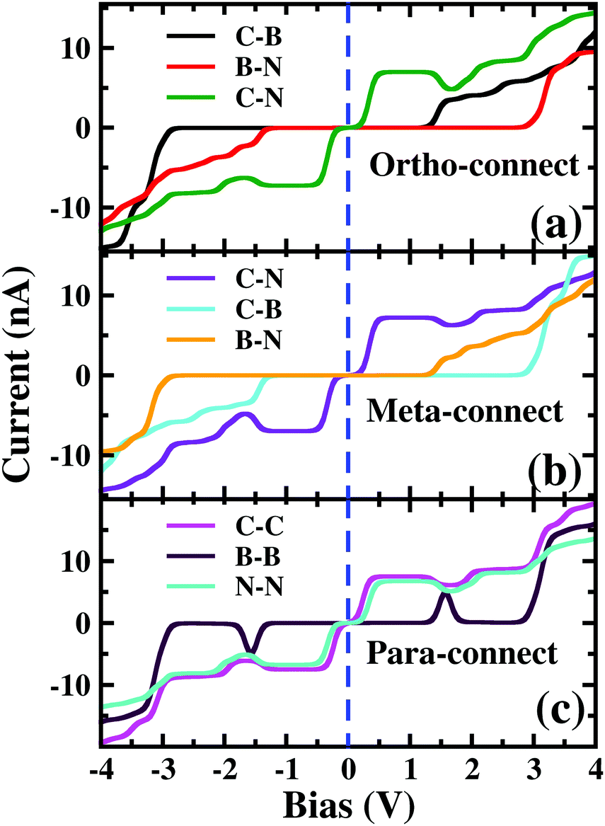 | ||
| Fig. 1 Current (I)–source-drain voltage (VSD) characteristics of a molecular device where the electrodes are connected in (a) ortho, (b) meta and (c) para-positions. The dashed blue line represents VSD = 0.0. In the upper left corner, the atomic sites attached to the electrodes are stated. See Fig. S3 in the ESI† for the detailed geometry of the electrode-molecule-electrode configurations. | ||
3.1 Negative differential conductance
First, we consider the molecular bridge with both para-positioned B atoms attached to the electrodes, para B–B (Fig. 1c). The I–V characteristic is identical at both the positive and negative bias, but with an opposite sign, which is I (VSD) = I (−VSD). This characteristic is obvious since both the geometry and strength of the molecule-electrode coupling are symmetrical in nature. This symmetrical I–V characteristic has already been observed for benzene and double quantum dot systems.21,33 Taking advantage of this symmetry, the I–V characteristics of the positive bias regime have been discussed further. As shown in the inset of Fig. 2(a), at low bias i.e. VSD < 1.0 V, the current appears to be very small, in the order of pA only. However, the most important feature of this nano-junction appears at the bias range of 1.0 V < VSD <2.2 V, where current rises sharply and then suddenly decreases with the increase in VSD, exhibiting a strong NDC behavior (see Fig. 2(a)). With further increase in bias, i.e. VSD > 2.80 V, the transport current steeply increases. Hettler et al. demonstrated similar NDC characteristics for a benzene-based molecular junction where the electrodes are weakly attached to the para-positions of the molecule.21 Experimentally, NDC has been demonstrated for molecular junctions with a variety of molecules such as polyporphyrine oligomers, nitroamine functionalized benzene, and azobenzene.10,34,35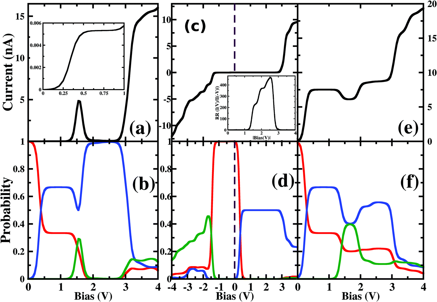 | ||
| Fig. 2 The variation of current (I) with VSD for the device at different positions in B2C2N2H6 (top panel in the figure) and the occupation probabilities in the bottom panel of the figure for the same configuration. (a) I–V for two boron atoms at the para position, (c) I–V for a boron and nitrogen atom at the ortho position and (e) I–V for two carbons at the para position. The occupation probabilities are represented by a red line for 6e-gs, a blue line for 7e-gs and a green line for 7e-1st-es states in (b), (d) and (f). In the inset of (a), the I–V plot for the junction connected by two borons has been shown for the bias-range 0.0 < VSD < 1.0 V. In the inset of (c), we include the rectification ratio (RR) of the molecular junction with varying bias. | ||
We further focus on the non-equilibrium occupation probabilities of transport-active many-body states and analyze how they are modified with a change in VSD to understand the NDC. As shown in Fig. 2(b), at 0.0 V < VSD < 0.2 V, the 6 electron ground-state (i.e. 6e-gs) remains almost completely populated, leaving all other states nearly empty. In this bias region, the applied VSD is not enough to charge the molecule with an extra electron, that is, the formation of the anion is not favoured. Due to the stable neutral charge state of the molecule within this energy range, there is no current through the molecular bridge and the device remains in the Coulomb blockade regime. As VSD increases, the 7 electron ground-state (i.e. 7e-gs) becomes energetically accessible and there is a transition of electrons from 6e-gs to 7e-gs, resulting in an increase in current (see Fig. 2(a and b)). However, unlike other molecules explored previously,21 the current due to this particular transition, appears to be very small, in the order of a few pA. This simply indicates that 7e-gs does not transport electrons through the present molecular device. With a further increase in VSD above a certain threshold bias-voltage, VSD > 1.15 V, the 7-electron first excited state (7e-1st-es) becomes accessible. Consequently, the corresponding occupation probability starts increasing and exhibits a sharp increase in the current for VSD > 1.30 V (see Fig. 2(a)). For further understanding, we calculate the transmission function as  , where ε = Es − Es′ is the transition energy. It can also be seen in Fig. 3 that the transmission function shows the first peak at the transition energy ε = E2 − E1 = 9.037 eV. This peak is due to the electronic transition from 6e-gs (E1 = −9.038 eV) to 7e-1st-es (E2 = −0.001 eV). Importantly, here, the magnitude of the current is in the order of nA, much higher than the current due to the tunnelling from 6e-gs to 7e-gs. At VSD > 1.55 V the probability of this conducting 7e-1st-es reduces, causing a sharp drop in the current. In this particular bias-voltage window, the transition from 7e-1st-es to the 6-electron first excited state (6e-1st-es) becomes energetically possible. Thus, the net occupation probability of 7e-1st-es starts reducing and for 6e-1st-es the probability should increase. However, as the transition from 6e-1st-es to 7e-gs is also probable at the same bias range, the net occupation probability of 7e-gs starts increasing as can be seen in Fig. 2(b). As 7e-gs is a weakly conducting state, the increase in the probability of it results in the reduction of transporting current, exhibiting the NDC.
 | ||
| Fig. 3 Transmission function as a function of transition energy (ε) for B–B and C–C para-connections. | ||
To understand the atomistic reason behind the different nature of 7-electron many-body states towards the electron transport in the sequential tunnelling regime, the charge densities of these states have been analyzed. As shown in Fig. 4, boron and nitrogen atoms in 6e-gs are electron deficient and rich, respectively, due to their intrinsic electronegativity. Interestingly, 7e-gs also has a similar electron density distribution where the state remains largely polar due to charge localization at nitrogen and charge depletion at boron sites, respectively. Hence, when the electrodes are connected to boron atoms at the para-position, the transition of the molecule from 6e-gs to 7e-gs at finite bias does not increase the electron-density at the electrode-molecule coupling region. And consequently, it results in a very weak current flow through the molecular junction. This explains the negligible current flow in the bias range of 0.0 < VSD <1.3 V and 1.85 < VSD <2.75 V in the junction as shown in Fig. 2 (a). On the other hand, in the 7e-1st-es, the electrons remain almost equally distributed over all the atomic sites. Thus, when the 7e-1st-es gets populated at a particular bias, the electron densities at B atoms increase appreciably, and the current with a magnitude of nA, flows through the molecular junction. This flow of current gets quenched at a higher bias (i.e. VSD >1.55 V) with population of the charge localized 7e-gs state. At a much higher bias i.e. VSD > 2.80 V, many more excited states start appearing as transport-active channels, rapidly growing the current (Fig. 2(a)).
 | ||
| Fig. 4 The charge density distribution of the 6-electron ground state, 7-electron ground state and 7-electron first excited state over the sites of B2C2N2H6. | ||
Thus, the population and depopulation of the anionic ground state and first excited state of B2C2N2H6, respectively, where the charge distribution patterns are different and decisive for current flow, result in an exciting non-linear behaviour of current–voltage characteristics.
3.2 Rectification
Considering the device with electrodes connected to chemically asymmetric ortho-positioned B and N atoms (ortho B–N), a prominent rectification of current is realised (Fig. 2(c)). Although at a positive bias regime, current with a magnitude of nA flows through the device, the negative bias regime shows nA current only after VSD = −2.80 V. We further calculate the rectification ratio (RR), which is defined as the ratio between the absolute current-values at positive and negative voltages,| RR(V) = |I(V)/I(−V)| | (2) |
The plotted rectification ratio in the inset of Fig. 2(c) shows it to be as high as 466.2 at 2.55 V. The occupation probability analysis of many-body states indicates that at negative bias, a major transition occurs between 6e-gs and 7e-1st-es, resulting in the flow of current at VSD < −1.25 V (see Fig. 2(c and d)). In this negative bias region, the 7e-gs remains almost empty. On the other hand, by applying a positive bias of VSD < 0.05 V, occupation probability decreases for 6e-gs and increases for 7e-gs. However, the current remains negligible until VSD < 2.80 V. After this threshold voltage, current starts flowing due to the increase of occupation probability of energetically higher lying conducting states.
Analyzing the charge density distribution per sites, in Fig. 4, it is evident that the boron site, attached with one of the electrodes, is electron deficient for 7e-gs. Thus, the occupation probability of 7e-gs eventually gives rise to unfavourable electron transport through the junction. However, for 7e-1st-es, both the connecting sites i.e. N and B are electron-rich and suitable for electron transport. So, the different occupation probability of these low-lying states at positive and negative biases results in prominent rectification in the device. Note that, similar current rectification also appears for other electrode-molecule conformations with chemically different atomic sites attached to the electrodes (Fig. 1).
3.3 Staircase
In the following section, we focus on the molecular junctions with electrodes attached to two carbon atoms in the para-position, para C–C. As in Fig. 2(e), a step-like I–V character emerges for this junction. This kind of I–V behaviour is common for junctions where sequential tunnelling is the major mechanism for electron transport. As discussed previously, in this sequential tunnelling regime, the charging energy of the molecule is high and needs to be overcome by applying a certain VSD. Before this threshold VSD, the device remains in the Coulomb blockade regime (see Fig. 2(e)). Furthermore, with an increase in VSD, 7e-gs starts filling up and electrons start flowing through the junction (Fig. 2(f)). It can also be seen in Fig. 3 that the transmission function shows the first peak at the transition energy ε = E3 − E1 = 8.478 eV. This peak is due to the electronic transition from 6e-gs (E1 = −9.038 eV) to 7e-gs (E3 = −0.56 eV). With an increase in VSD, other excited states of different charge and spin sectors become accessible, resulting in steps in the I–V character.Importantly, as the electrodes are connected to two carbon atoms which are electron-rich for 7e-gs, current flows through the molecular junctions when there is an increased VSD at this anionic state. A small dip in the current at 1.1 V < VSD < 2.0 V appears due to the finite occupation probability of 7e-1st-es, which is less favourable towards electron transport in the present conformation. Less electron density at the carbon sites reduces the conducting nature of 7e-1st-es compared with that of 7e-gs.
Furthermore, the device with para N–N also exhibits a similar staircase I–V character (Fig. 1(c)).
3.4 Effect of magnetic field
In this section, the effect of the perpendicular magnetic field on molecular conductance has been explored. For para B–B conformation, at a relatively small magnetic field strength, 0.001ϕ0 < ϕ < 0.02ϕ0, the current increases at a low bias (0.15 V < VSD < 0.50 V) region with the magnetic field (Fig. 5(a)). However, it is to be noted that the magnitude of the resulting current remains in the pA order. The prominent NDC also remains almost unaltered under these relatively small magnetic fields. Interestingly, as we increase the magnetic field strength further, i.e. 0.02ϕ0 < ϕ < 0.10ϕ0, the current conduction starts changing at the NDC-peak region i.e. 1.0 V < VSD < 3.0 V (see Fig. 5(c)). Applying a magnetic field of ϕ < 0.14ϕ0, the NDC-peak almost disappears and I–V exhibits staircase behaviour. Thus, depending on the strength of the magnetic field, the transport characteristics of this molecular junction can be controlled drastically. | ||
| Fig. 5 (a) I–V characteristics for the low bias regime (VSD of 0 V < VSD < 1.0 V) versus magnetic field strength for paratha para-positioned boron connected device. (b) Charge density at the boron sites with varying magnetic field strength. (c) I–V characteristics and (d) occupation probabilities of 7e-1st-es at higher VSD, for varying magnetic field strength. | ||
To understand the modulation in I–V characteristics, we now concentrate on two majorly sensitive factors, which get modified with applied magnetic fields; (1) the change in charge distribution on the atomic-sites of the molecule and (2) the occupation probabilities of transport-relevant six- and seven-electron many-body states.
On applying a relatively small magnetic field, 0.001ϕ0 < ϕ < 0.02ϕ0, the occupation probabilities of low-lying 6e and 7e-states remain almost unaltered. However, the charge distribution on the atomic sites gets modified in these states. Most importantly, as in Fig. 5(b), B-sites in the 7e-gs start getting populated under the application of a magnetic field. The charge density at B-sites for 7e-gs keeps on increasing with the applied magnetic field. This increase in electron density on B-sites in turn makes 7e-gs suitable for current conduction. Thus, at low-bias (0.15 V < VSD < 0.50 V) where 6e-gs to 7e-gs transition occurs, the amplitude of the resulting current keeps on increasing with the applied magnetic field. However, as under a weak magnetic field, the increase in the charge on B-atoms is small, ≈2 × 10⁻⁴e−, and the resulting current remains in pA only (see Fig. 5). Thus, it is evident that current through a boron-connected molecular junction increases with the accumulation of charge-densities at boron-sites.
As shown in Fig. 5(c), with a higher applied magnetic field, 0.02ϕ0 < ϕ < 0.13ϕ0, when the prominent NDC peak gets affected, the current does not completely switch-off at VSD < 1.80 V. As the B-site of 7e-gs keeps on getting populated under a stronger magnetic field, the current increases at the bias range of 0.15 V < VSD < 0.50 V as discussed previously. It is apparent from Fig. 5(d) that although the occupation probability of highly conducting 7e-1st-es at VSD < 1.55 V reduces, unlike previously, it remains finite at the bias range, VSD < 1.80 V. As this highly conducting state remains populated at the higher bias, the current never drops down to zero at any higher bias. Moreover, since 7e-gs is also conducting, high occupation of this state further results in a measurable current flow through the molecular junction. Thus, at higher magnetic field strength, both charge densities at atomic sites and occupation probabilities of current-conducting states are modulated, resulting in a change in the I–V characteristics.
Under a higher magnetic field i.e. ϕ < 0.14ϕ0, as shown in Fig. 6, the NDC disappears completely and shows staircase behaviour. In these magnetic fields, at low-bias i.e. VSD < 0.20 V the current gets switched-on and keeps on increasing as the bias-voltage increases in a step-wise manner. From the occupation probability, it is evident that current flow at a low-bias is assisted by 6e-gs to 7e-gs transition, as mentioned earlier. Importantly, as the 7e-gs is now suitable for current conduction, at higher VSD when the occupation probability of the major conducting state 7e-1st-es reduces and that of 7e-gs increases, staircase behaviour appears. Thus, there is no NDC in the I–V characteristics in the presence of a higher magnetic field.
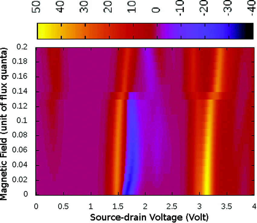 | ||
| Fig. 6 The colour map shows differential conductance (dI/dV) as a function of VSD and applied perpendicular magnetic field (ϕ) for the para-positioned boron connected device. | ||
Generally, it has been believed that the magnetic flux needed to affect the molecular conduction is of the order of a magnetic flux quanta and the required magnetic field is unrealistically high in magnitude.25 However, in the present study the bias-dependent occupation probabilities and charge densities of transport active many-body states are highly sensitive to the magnetic field. Thus, we realize significant modifications in transport characteristics, even under relatively weak magnetic perturbation. By analyzing the I–V characteristics of other molecule-electrode conformations, we find that the magnetic field has very little effect on the I–V characteristics in these cases.
The other perturbing factor, applied gate voltage, can also significantly affect the resulting current. Particularly, the molecular junction with prominent NDC character in the absence of gate voltage exhibits significant modification in the net current flow upon the application of gate-voltage. As in Fig. 7, the negative differential conducting nature can efficiently be switched off and on by varying the strength of the applied gate voltage. Note that the strength of the gate voltage used in the present study has been regularly achieved in experiments. Looking at the probability distribution, it becomes evident that as the strength of the gate voltage increases, the probability of conducting 7e-1st-es around 1.0 V < VSD < 2.0 V gets diminished. Consequently, the NDC peak also disappears. Transition rates among the transport active many-body states (6e-gs to 7e-1st-es in the present system) and their relative energies compared to the electrodes fundamentally cause these kinds of alterations in the I–V characteristics.
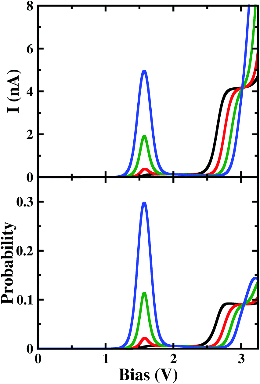 | ||
| Fig. 7 The upper panel shows the I–V characteristic of the boron-electrode connected junction at different gate voltages. The lower panel depicts the occupation probability of 7e-1st-es at 0.0 V < VSD < 3.5 V where different gate voltages have been applied. Black, red, green and blue solid lines represent the current (upper panel) and the probability (lower panel) with applied gate voltages of 0.15 V, 0.10 V, 0.05 V and 0 V, respectively. | ||
Chemical substitution for hydrogen atoms with different electropositive or electronegative functional groups is another powerful approach to control the transport characteristics of the weakly coupled molecular junctions.36–40 Fundamentally, the functionalization of molecules can fine-tune the on-site energy of the particular atom that gets attached to the functional group, tuning the chemical environment of the transporting ring. In this regard, fluorination of molecules has been studied widely due to its high electronegativity, which can change the on-site energy of atoms in the ring substantially.41–44 Galen et al. demonstrate that selective fluorination on particular positions of biphenylethane-based molecules can introduce a strong current rectification character.45 However, we are not investigating the impact of chemical functionalization on the non-linear characteristics of molecular transport as this topic needs extensive simulations and is out of the scope of our present study.
4. Conclusions
To conclude, we have discussed the transport characteristics of B2C2N2H6 molecular systems in a sequential tunnelling regime, applying a well-established kinetic equation approach. We find that the I–V character of this molecule strongly depends on the atomic nature of the sites, which are connected to the electrodes. When both B atoms are used as connecting sites, NDC appears in the device, whereas with two different chemical species as the connecting site, prominent rectification of current emerges. All this exciting non-linear transport arises due to the VSD-dependent population and depopulation of low-lying excited states, which are quite different in terms of charge distribution patterns and hence the nature of electron conduction. The molecules of these transport active many-body states determine the I–V characteristics. Particularly, the charge densities at the connecting sites to the electrode dominantly control the current conduction through the molecular junctions. Furthermore, a perpendicular magnetic field also substantially modulates the current conduction. All these exciting computational studies and in-depth understanding will certainly guide the experimental efforts in building small molecule-based devices for next-generation nanoelectronics.Conflicts of interest
There are no conflicts to declare.Acknowledgements
P. P. acknowledges DST-SERB (ECR/2017/003305) for the financial support. S. K. P. acknowledges DST for the financial support.References
- D. Xiang, X. Wang, C. Jia, T. Lee and X. Guo, Chem. Rev., 2016, 116, 4318–4440 CrossRef CAS PubMed.
- A. Vilan, D. Aswal and D. Cahen, Chem. Rev., 2017, 117, 4248–4286 CrossRef CAS PubMed.
- R. J. Nichols and S. J. Higgins, Annu. Rev. Anal. Chem., 2015, 8, 389–417 CrossRef CAS PubMed.
- H. Jeong, D. Kim, D. Xiang and T. Lee, ACS Nano, 2017, 11, 6511–6548 CrossRef CAS PubMed.
- S. V. Aradhya and L. Venkataraman, Nat. Nanotechnol., 2013, 8, 399 CrossRef CAS PubMed.
- C. Lambert, Chem. Soc. Rev., 2015, 44, 875–888 RSC.
- J. R. Heath and M. A. Ratner, Mol. Electron., 2003 Search PubMed.
- G. Cuniberti, G. Fagas and K. Richter, Introducing molecular electronics: A brief overview, Springer, 2006 Search PubMed.
- J. L. Zhang, J. Q. Zhong, J. D. Lin, W. P. Hu, K. Wu, G. Q. Xu, A. T. Wee and W. Chen, Chem. Soc. Rev., 2015, 44, 2998–3022 RSC.
- J. Chen, M. Reed, A. Rawlett and J. Tour, Science, 1999, 286, 1550–1552 CrossRef CAS PubMed.
- M. L. Perrin, R. Frisenda, M. Koole, J. S. Seldenthuis, J. A. C. Gil, H. Valkenier, J. C. Hummelen, N. Renaud, F. C. Grozema and J. M. Thijssen, et al. , Nat. Nanotechnol., 2014, 9, 830 CrossRef CAS PubMed.
- B. Xu and Y. Dubi, J. Phys.: Condens. Matter, 2015, 27, 263202 CrossRef PubMed.
- J. Liu and D. Segal, Nano Lett., 2020, 20, 6128–6134 CrossRef CAS PubMed.
- R. M. Metzger, Chem. Rev., 2015, 115, 5056–5115 CrossRef CAS PubMed.
- C. Van Dyck and M. A. Ratner, Nano Lett., 2015, 15, 1577–1584 CrossRef CAS PubMed.
- S. Sanvito, Chem. Soc. Rev., 2011, 40, 3336–3355 RSC.
- A. R. Rocha, V. M. Garcia-Suarez, S. W. Bailey, C. J. Lambert, J. Ferrer and S. Sanvito, Nat. Mater., 2005, 4, 335–339 CrossRef CAS PubMed.
- D. Aravena and E. Ruiz, J. Am. Chem. Soc., 2011, 134, 777–779 CrossRef PubMed.
- Y. Dubi and M. Di Ventra, Rev. Mod. Phys., 2011, 83, 131 CrossRef CAS.
- J. Park, A. N. Pasupathy, J. I. Goldsmith, C. Chang, Y. Yaish, J. R. Petta, M. Rinkoski, J. P. Sethna, H. D. Abruña and P. L. McEuen, et al. , Nature, 2002, 417, 722–725 CrossRef CAS PubMed.
- M. Hettler, W. Wenzel, M. Wegewijs and H. Schoeller, Phys. Rev. Lett., 2003, 90, 076805 CrossRef CAS PubMed.
- P. Parida, S. Lakshmi and S. K. Pati, J. Phys.: Condens. Matter, 2009, 21, 095301 CrossRef PubMed.
- K. Ono and S. Tarucha, Phys. Rev. Lett., 2004, 92, 256803 CrossRef PubMed.
- S. Lakshmi, S. Dutta and S. K. Pati, J. Phys. Chem. C, 2008, 112, 14718–14730 CrossRef CAS.
- D. Rai, O. Hod and A. Nitzan, J. Phys. Chem. Lett., 2011, 2, 2118–2124 CrossRef CAS.
- B. Wang, Y. Li, R. Ganguly, H. Hirao and R. Kinjo, Nat. Commun., 2016, 7, 11871 CrossRef CAS PubMed.
- V. Marcon, O. A. von Lilienfeld and D. Andrienko, J. Chem. Phys., 2007, 127, 064305 CrossRef PubMed.
- A. K. Srivastava, S. K. Pandey and N. Misra, Theor. Chem. Acc., 2016, 135, 1–7 Search PubMed.
- Y. A. Pati and S. Ramasesha, J. Phys. Chem. A, 2014, 118, 4048–4055 CrossRef CAS PubMed.
- J. E. Sansonetti, W. Martin and S. Young, Carbon, 2005, 100, 1634 Search PubMed.
- K. Wakabayashi, M. Fujita, H. Ajiki and M. Sigrist, Phys. Rev. B: Condens. Matter Mater. Phys., 1999, 59, 8271 CrossRef CAS.
- C. Rocha, A. Latgé and L. Chico, Phys. Rev. B: Condens. Matter Mater. Phys., 2005, 72, 085419 CrossRef.
- B. Muralidharan and S. Datta, Phys. Rev. B: Condens. Matter Mater. Phys., 2007, 76, 035432 CrossRef.
- G. Kuang, S. Z. Chen, L. Yan, K. Q. Chen, X. Shang, P. N. Liu and N. Lin, J. Am. Chem. Soc., 2018, 140, 570–573 CrossRef CAS PubMed.
- B.-Y. Choi, S.-J. Kahng, S. Kim, H. Kim, H. W. Kim, Y. J. Song, J. Ihm and Y. Kuk, Phys. Rev. Lett., 2006, 96, 156106 CrossRef PubMed.
- M. L. Perrin, R. Eelkema, J. Thijssen, F. C. Grozema and H. S. van Der Zant, Phys. Chem. Chem. Phys., 2020, 22, 12849–12866 RSC.
- C. Van Dyck and A. J. Bergren, Adv. Electron. Mater., 2018, 4, 1700656 CrossRef.
- X. Chen, H. V. Annadata, B. Kretz, M. Zharnikov, X. Chi, X. Yu, D. A. Egger and C. A. Nijhuis, J. Phys. Chem. Lett., 2019, 10, 4142–4147 CrossRef CAS PubMed.
- H. Valkenier, C. M. Guédon, T. Markussen, K. S. Thygesen, S. J. van der Molen and J. C. Hummelen, Phys. Chem. Chem. Phys., 2014, 16, 653–662 RSC.
- P. Gehring, J. M. Thijssen and H. S. van der Zant, Nat. Rev. Phys., 2019, 1, 381–396 CrossRef.
- M. L. Perrin, E. Galán, R. Eelkema, J. M. Thijssen, F. Grozema and H. S. van der Zant, Nanoscale, 2016, 8, 8919–8923 RSC.
- A. Asyuda, X. Wan and M. Zharnikov, Phys. Chem. Chem. Phys., 2020, 22, 10957–10967 RSC.
- A. Asyuda, A. Wiesner, X. Wan, A. Terfort and M. Zharnikov, J. Phys. Chem. C, 2020, 124, 24837–24848 CrossRef CAS.
- P. Werner, T. Wachter, A. Asyuda, A. Wiesner, M. Kind, M. Bolte, L. Weinhardt, A. Terfort and M. Zharnikov, ACS Appl. Mater. Interfaces, 2020, 12, 39859–39869 CrossRef CAS.
- E. Galán, M. L. Perrin, M. Lutz, H. S. Van Der Zant, F. C. Grozema and R. Eelkema, Org. Biomol. Chem., 2016, 14, 2439–2443 RSC.
Footnotes |
| † Electronic supplementary information (ESI) available: Details of the computational methods, optimized electrode-molecule geometry, charge densities of valence and conduction band edges, and position of the electrodes in electrode-molecule-electrode junctions. See DOI: 10.1039/d1tc01092a |
| ‡ Current Address: Theoretical Division and Center for Nonlinear Studies, Los Alamos National Laboratory, Los Alamos, NM, 87545, USA. |
| This journal is © The Royal Society of Chemistry 2021 |