
 Open Access Article
 This Open Access Article is licensed under a
 Creative Commons Attribution 3.0 Unported Licence
Colour-encoded electroluminescent white light-emitting diodes enabled using perovskite–Cu–In–S quantum composites†
Seung-Bum
Cho‡
a,
Jung Inn
Sohn‡
 b,
Sang-Seok
Lee
a,
Seung-Gyun
Moon
a,
Bo
Hou
*c and
Il-Kyu
Park
*a
b,
Sang-Seok
Lee
a,
Seung-Gyun
Moon
a,
Bo
Hou
*c and
Il-Kyu
Park
*a
aDepartment of Materials Science and Engineering, Seoul National University of Science and Technology, Seoul 01811, Republic of Korea. E-mail: pik@seoultech.ac.kr
bDivision of Physics and Semiconductor Science, Dongguk University, Seoul, Republic of Korea
cDepartment of Physics and Astronomy, Cardiff University, Cardiff CF24 3AA, UK. E-mail: HouB6@cardiff.ac.uk
First published on 24th April 2021
Abstract
Solution-processed quantum dot (QD) white light-emitting diodes (WLEDs) have received much attention as viable light sources in next-generation large-area ambient lighting, flexible photonics and full-colour display backlighting technologies. Attributable to their solution processibility, tunable colour temperature, high quantum efficiency and high photostability, considerable research efforts have been spent on accumulating new insights into materials and device architecture design for high-performance QD WLEDs. At present, prevalent research on WLEDs focuses on using QDs as photoluminescence colour converters or using purely narrow linewidth QD LEDs to complement the white light spectrum, which is not energy efficient as well as challenging to achieve Eye Comfort ambient colour coding. Herein, a quantum composite made by hybridising perovskite (CsPbBr3 and CsPb(Br1−xClx)3) and CuInS2 (CIS) QDs is proposed as a colour-encoded electroluminescent layer, which underpins good white colour temperature and bias stability for ambient lighting. Instead of using solely sharp emission QDs to match the white light spectrum, broad light emission spectrum CIS QDs are used for colour temperature tuning. In addition, the mixed-halide perovskite CsPb(Br1−xClx)3 QDs are successfully synthesised through a noninvasive halide ion exchange method associated with trimethylsilyl chloride additives, which provide a good colour purity in the blue and green electroluminescence regions. These designed QD composites enable the as-prepared WLED electroluminescence spectra to match the ideal ambient light Commission International de l’Éclairage 1931 (CIE) colour coordinates with a mean value of 0.33, 0.34. Moreover, the as-prepared WLEDs show a turn-on voltage of 4 V with negligibly small leakage current, good colour stability and electrical bias tolerance even under a broad range of driving voltages. Our results herald the advent of molecular level hybridisation of different quantum materials for high-performance electroluminescence white colour toning.
Introduction
Colloidal inorganic quantum dot (QD)-based light-emitting diodes (QLEDs) have emerged as promising candidates for flexible full-colour displays and large-area lighting due to their unique properties, such as total solution processibility, tunable colour temperature, low driving voltages, high luminous efficiency, and high brightness.1–8 The past decades have shown tremendous advances in QD technology, allowing for the design of efficient QD materials and device structures. QLEDs have approached the state-of-the-art performance of organic LEDs.5 This, in turn, allows for creating new device architectures of QD-based white light-emitting diodes (WLEDs) pertinent to future displays and ambient lighting.2To date, two main approaches have been generally adopted to deploy QDs for WLED applications. The prevalent one is using QDs as a photoconversion layer instead of conventionally used inorganic phosphor materials.4,5 However, this approach is required to properly combine the converted blue light from a GaN-based LED chip and the remaining transmitted blue light to generate QD photoluminescence white emission. Moreover, there remain inevitable problems, such as their low colour rendering index,9 intrinsic energy loss due to several conversion processes,10 low colour stability,11,12 and thermal quenching of the QDs.11,12 The other one is developed by using QDs as an active layer of the electroluminescent WLED, which is capable of emitting desirable multiple colours from various QDs themselves to complete a white colour emission.6–8 This electroluminescence approach could provide more flexibility towards achieving superior colour efficiency with better colour stability and colour temperature customizability in the development of QD-based WLEDs.2
Recently, some reports demonstrated all-QD-based WLEDs with emissive layer structures formed by stacking red, green, and blue QD multilayers vertically or by building a tandem structure with the introduction of interconnecting transfer layers.6–8 However, these structures also suffer from several challenges such as nonradiative Auger recombination, Förster resonant energy transfer of excitons to nonradiative sites before recombination, the imbalance between hole and electron transport, and voltage-dependent colour variations as well as the complicated and sophisticated multiple layer deposition processes.13,14 In addition to these structure issues, there are also severe impediments to the employment of Cd-based II–VI QDs in these reported WLEDs.2 Though these Cd-based QDs have been widely used and have demonstrated electroluminescence performance comparable to the latest OLEDs,9 the toxic and environmental issues of Cd still remain considerable challenges for their broad deployment.15,16
As an alternative luminescent quantum material system, cesium lead halide (CsPbX3; X = Cl, Br, and I) based all-inorganic perovskite QDs have attracted much attention due to their excellent and unique optoelectronic properties, such as small exciton binding energy, high photoluminescence quantum yields (PLQYs), superior band structures with a defect tolerance, and wide bandgap tunability covering the ultraviolet to infrared wavelength spectral ranges.17–21 CsPbBr3 QD-based green LEDs have shown impressive progress, with external quantum efficiencies (EQEs) exceeding more than 16%, but relatively little research has been done on investigation of WLEDs using these materials.2,19 Recently, Yao et al. demonstrated a WLED fabricated with blue light-emitting CsPbBrxCl3−x QDs, an orange light-emitting polymer, and poly[2-methoxy-5-(2-ethylhexyloxy)-1,4-phenylenevinylene] (MEH:PPV).22 Besides, Mao et al. also demonstrated a WLED by stacking cyan light emitting CsPb(Br,Cl)3 and red light-emitting (CH3CH2CH2NH3)2CsPb2I7 nanosheet structures.23 However, serious hurdles remain in using perovskite QDs purely to cover the whole white spectrum, such as low efficiency and poor stability against moisture, heat, oxygen, and electric fields.2,18 In addition, to realize a genuinely white colour emission, the colour and bandwidth of each colour component need to be encoded. For instance, instead of sharp red emission used in previous studies, a broader red emission bandwidth is theoretically preferred to obtain a warm white emission.2 Also, the stability issue is another critical issue that needs to be considered, which usually results in device performance deterioration, a loss of efficiency, and colour changes.2 Therefore, it is necessary to seek an effective and alternative strategy to achieve more stable and electroluminescence white colour emission from QD-based WLEDs.
Herein, we propose and demonstrate a new approach for all-QD-based WLEDs with good colour stability by introducing a hybrid material structure formed by blending halide perovskite QDs (CsPbBr3 and CsPb(Br1−xClx)3) with CuInS2 (CIS) QDs. This self-emissive QD hybrid has been used to generate white electroluminescence with the colour balance between blue (472 nm), green (506 nm), and orange (620 nm), which is well-matched with the Commission International de l’Éclairage 1931 (CIE) colour coordinates with a mean value of 0.33, 0.34. We also performed comprehensive spectroscopy characterisation studies to elucidate the principles of our colour coding approach. We demonstrate that the single emissive layer containing elaborately designed perovskite–Cu–In–S quantum composites can achieve customised colour coordinates for typical white lighting associated with simultaneous carrier injections, recombinations, and light emissions from each emissive QD.
Results and discussion
In this work, CsPbBr3 and CsPb(Br1−xClx)3 QDs were prepared by the previously reported ligand-assisted method and anion exchange method for green and blue light-emitting layers, respectively.17 The anion exchange reaction was performed by adding trimethylsilyl chloride (TMSC) into the pristine CsPbBr3 QDs. For the orange and red light-emitting layers, stable and broad emission linewidth CIS QDs were selected and used instead of sharp emission CsPbI3-based perovskite QDs that have low stability and halide anion exchange problems.18 Considering the colour toning, various mass ratios of orange, red, green, and blue light-emitting QDs were blended in n-octane (10 mg mL−1 concentration) to form a single blended self-emissive QD layer. The bottom emitting device structure was demonstrated by employing poly(3,4-ethylene dioxythiophene):polystyrene sulfonate (PEDOT:PSS) as a transparent hole injection layer, as shown in Fig. 1a. Poly-n-vinyl carbazole (PVK) and ZnO nanoparticles (NPs) served as a hole-transport layer (HTL) and an electron-transport layer (ETL), respectively. As shown in the LED's energy band structure (Fig. 1b), the PVK acted as a hole-transporting and electron-blocking layer simultaneously because it has low electron affinity (2.2 eV). Positive and negative charge carriers were recombined in a thin blended emissive QD layer under forward bias, where they generated short and long wavelength photons simultaneously. The fabricated LED device showed a flat surface without showing any layers’ delamination (Fig. 1c). The blended QD films showed a homogeneous uniform surface (Fig. 1d). The structural architecture of QD WLED devices was characterised using the cross-sectional high-resolution SEM image in Fig. 1d, where the multiple layers were arranged and configured in sequential order as we designed: indium-doped tin oxide (ITO), PEDOT:PSS (30 nm), PVK (30 nm), QD composites (30 nm), ZnO NPs (50 nm), and Al (100 nm). | ||
| Fig. 1 (a) Schematic structure of the QD-based WLED device. (b) Energy band structure of the QD-based WLED device. (c) Photo image of WLEDs. The inset shows the spin-coated QD thin films on a PVK/PEDOT:PSS/ITO/glass substrate. (d) Cross-sectional high-resolution SEM image of the full structure of the QD-based WLED device. The inset shows the spin-coated QD thin films exhibiting uniform and flat surfaces. | ||
The structural properties of the QDs were assessed using transmission electron microscopy (TEM) and high-resolution TEM (HR-TEM). The TEM image of the CsPbBr3 QDs shows a purely cubic morphology and uniform size distribution with an average diameter of 9 nm (Fig. 2a). Even after the TMSC treatment, it was observed that there is no significant change in particle shapes or sizes except for the halide composition (Fig. 2b). Previous studies reported that the chemical additives did not affect the crystallographic structure or crystallinity except for anion composition.24–26 The pristine and TMSC-treated CsPbBr3 QDs clearly showed well-defined lattice fringes in the high-resolution HR-TEM image, indicating the high crystalline quality of the QDs.
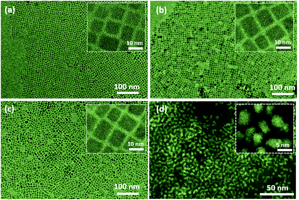 | ||
| Fig. 2 (a) TEM images of the QDs: (a) green light emitting pristine CsPbBr3 QDs, (b) blue light emitting CsPb(Br1−xClx)3 QDs, (c) blended cyan light emitting CsPb(Br1−xClx)3 QDs, and (d) red light emitting CIS QDs. | ||
Moreover, it can be seen that the mixed blue and green light-emitting perovskite QDs showed similar features to the pristine and TMSC-treated perovskite QDs without showing any agglomeration (Fig. 2c). The chlorine and bromine ions have been exchanged noninvasively, where the chlorine ion diffuses into the inner lattice sites of the CsPb(Br1−xClx)3 QDs so that they can form a thoroughly mixed halide alloy without phase transitions. Even in the absence of additional halide sources, the QDs themselves can serve as halide sources for each other. For example, the mixing of CsPbBr3 and CsPbI3 in colloidal solution resulted in fast cross-exchange and homogenisation of their compositions, forming CsPb(Br1−xIx)3 solid solutions.26,27 However, mixing the CsPbBr3 and CsPb(Br1−xClx)3 QDs does not induce halide exchange. This can be inferred from the dual PL peaks corresponding to the two types of QDs observed after mixing the QDs in the solution. As shown in Fig. 2d, the TEM image shows that the CIS QDs are monodispersed. Meanwhile, the HR-TEM data (inset) also demonstrate the good crystallinity of the as-prepared CIS QDs. The mixture of the perovskite and CIS QDs is homogeneously dispersed with preserved morphologies and crystallinity (Fig. S1–S3, ESI†).
The CsPbBr3 QDs showed a strong photoluminescence (PL) emission peak at 510 nm with a full width at half-maximum (FWHM) of 32 nm (Fig. 3b). The PL emission peak is slightly blue-shifted compared to the bandgap of bulk CsPbBr3 (2.42 eV) due to the weak quantum confinement effect because QDs with diameters very close to the exciton Bohr diameters of CsPbBr3 (7 nm) can benefit from the quantum confinement effect.17,21 4 μL of TMSC-treated CsPbBr3 QDs showed a PL peak at 485 nm due to the increased chlorine content (Fig. 3a). The CIS QDs showed PL emission peaks at 629 and 681 nm due to the quantum confinement effect depending on their size (Fig. 3c and d).
 | ||
| Fig. 3 PL spectra and emission images of the QD solutions: (a) blue light-emitting CsPb(Br1−xClx)3 QDs, (b) green light-emitting pristine CsPbBr3 QDs, (c) orange light-emitting CIS QDs, and (d) red light-emitting CIS QDs. PL spectra of the QD thin films of (e) blue light-emitting CsPb(Br1−xClx)3 QDs, (f) green light-emitting pristine CsPbBr3 QDs, (g) orange light-emitting CIS QDs, and (h) red light-emitting CIS QDs. The insets show the emission images under illumination with a 405 nm laser. | ||
To further evaluate their emission behavior, QD thin films were deposited by spin-coating the solutions on a double side polished sapphire substrate. As shown in the emission images, the thin films showed strong blue, green, orange, and red light with uniform emission distributions on the whole of the surfaces. Fig. 3e–h show the PL spectra of the blue, green, orange, and red light-emitting QD thin films, respectively. As TMSC was added, the PL emission peaks showed a blue-shift from 505 to 472 nm. The PL emission bandwidth also decreased, which indicates that the size distribution and composition of the QDs become more uniform, and there is a negligible amount of defect states that are related to nonradiative recombination.28–30 The orange and red light-emitting CIS QD films showed PL peaks at 621 and 679 nm, respectively. It should be noted that the PL emission peaks of the CIS QD film also showed a slight blue-shift compared to its solution state. The reason for such a blue-shift phenomenon is not clear but might be ascribed to the following factors: (i) QD surface reconstruction or surface oxidation;31,32 (ii) hydrostatic compression of QDs in the film state;33,34 or (iii) easy removal of larger QDs using syringe filters during the spin-coating process.35
To explore the optimal colour coding for the white light emission, blue, green, and red light-emitting QDs were mixed with various volume ratios. Fig. 4a shows the PL spectra of the perovskite and CIS blended solutions. The PL spectra showed three emission peaks centered at 480, 520, and 680 nm, which correspond to the CsPb(BrxCl1−x)3, CsPbBr3 perovskite QDs and red CIS QDs, respectively. This observation indicates that there are no changes in the emission peaks after hybridising the CsPb(Br1−xClx)3 and CIS QDs, which exclude the possibility of undesired side reaction or Förster resonant energy transfer between them. The optical absorption spectra for the perovskite–CIS composite showed distinct absorption features, which correspond to orange, green, and blue light-emitting QD regions (Fig. S4, ESI†). These results also imply that the halide exchange between the CsPb(Br1−xClx)3 and CsPbBr3 QDs is suppressed due to the steric hindrance and binding energy difference between surface ligands. As the portion of red CIS QDs enriched, a monotonic increase of the red emission peak could be observed. The PL emission colour of the perovskite–CIS composite was further quantified by evaluating the Commission International de l’Éclairage 1931 (CIE) coordinates as a function of the CsPb(Br1−xClx) to CIS ratio (Fig. 4b). The CIE coordinates shifted from (0.21, 0.34) to (0.52, 0.36) with the red QD content increasing from 0.25 to 4. As shown in the inset of Fig. 4a, the emission colour changed from bluish-white to reddish-white with increasing red CIS QD content (Table S1, ESI†). Based on this colour coding principle, the white colour temperature of the perovskite–CIS composite solutions could be well-modulated. To evaluate its colour stability, the excitation power-dependent PL spectra of the perovskite–CIS composite solution (B1G1R1) were also characterised by controlling the excitation laser power from 70 to 90 mW. Upon increasing the excitation laser power, the PL spectra showed similar shapes with slightly saturated red emission. The CIE coordinates changed from (0.27, 0.34) to (0.21, 0.31) when increasing the excitation laser power from 70 to 90 mW. This could be due to the relatively higher PLQYs of the blue and green CsPb(Br1−xClx)3 QDs than that of the red CIS QDs, which shift the CIE coordinates to the lower region.
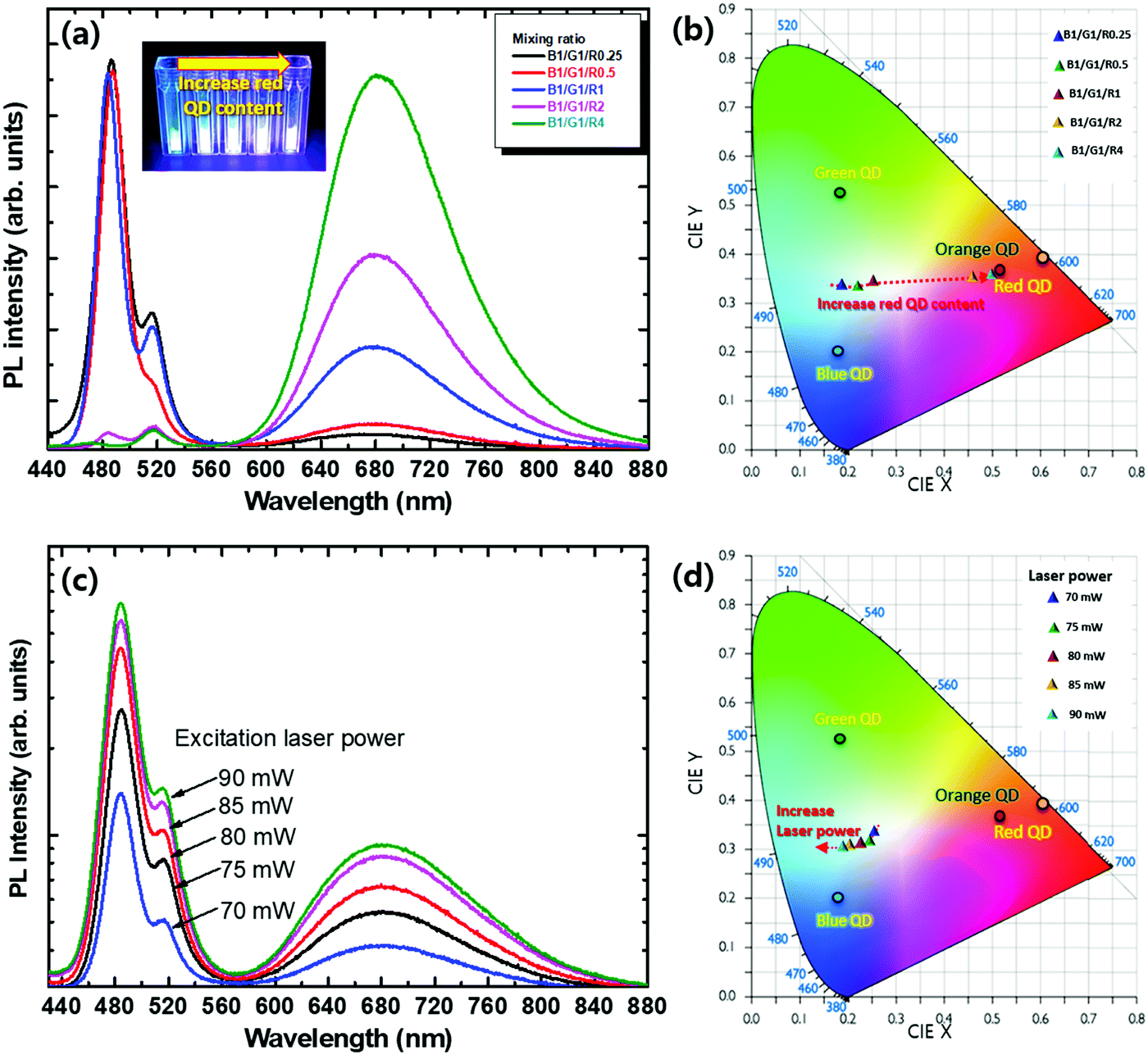 | ||
Fig. 4 (a) PL spectra and emission images of the blended QD solutions with various mixing ratios. (b) CIE coordinates of the PL emission colours with various mixing ratios. (c) The excitation power-dependent PL spectra and (d) CIE coordinates of the PL emission colours for a blended QD solution of blue, green, and red light-emitting QDs with a ratio of 1![[thin space (1/6-em)]](https://www.rsc.org/images/entities/char_2009.gif) :1:1. :1:1. | ||
A WLED device was fabricated based on the selected perovskite and CIS QDs. The orange light emitting CIS QDs (629 nm) were used by considering the emission wavelengths of the blue and green light emitting perovskite QDs. The as-prepared WLED was assembled using a typical QLED configuration (Fig. 1a) which consists of ITO/PEDOT:PSS/PVK/QD composites/ZnO/Al. Fig. 5a shows the dark current density–voltage (J–V) characteristics of the WLED. The WLED showed a turn-on voltage of around 4 V and negligibly small reverse leakage current, which are similar to the characteristics of purely CsPbBr3 based green LEDs.17,22,25 To compare the device performances, we fabricated blue, green, and orange light-emitting QD-based LEDs. Compared with the perovskite QD-based blue and green LEDs, the CIS QD-based orange-red LED showed relatively larger electrical resistance (Fig. S5, ESI†). This relatively lower current density of the orange light-emitting CIS QD-based LED would be due to the insulating behavior of the longer ligands on the CIS QDs. The WLED based on the perovskite and CIS quantum composites showed much lower current density than the devices with individual QDs. For the fabrication of CIS QD-based devices, we usually remove long ligands on the QD surfaces by washing off the excess ligands with an acetonitrile solvent after spin coating. In this work, however, the washing step was omitted to prevent any damage to perovskite QDs. The residual excess ligands in the QD composite film layers would result in the reduced current density of the WLED with the perovskite and CIS quantum composites.
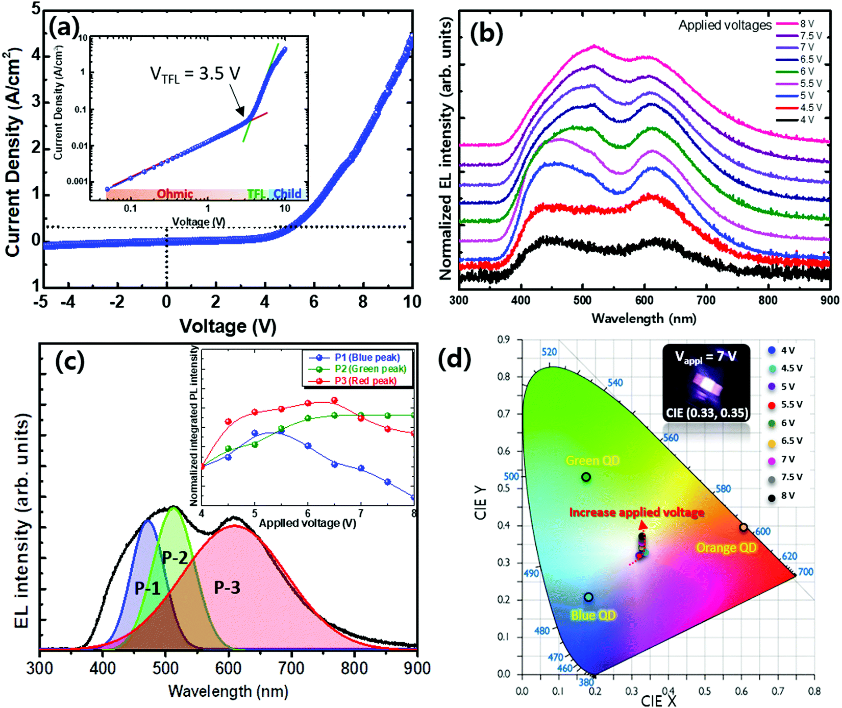 | ||
| Fig. 5 (a) The linear J–V curve of the QD-based WLED. The inset shows the logarithmic J–V curve. (b) Normalised EL spectra of the QD-based WLED with the variation of the applied bias. (c) EL spectrum of the WLED under an applied bias of 7 V. Three elementary EL spectra shown by coloured lines are obtained by deconvoluting the EL spectrum of the WLED. The inset shows the normalised EL intensities of the P1, P2, and P3 elementary peaks with the variation of the applied bias and their intensity ratio. (d) CIE coordinates of the EL emission colours measured at various applied bias voltages from 4 to 8 V. The inset shows the EL emission image under 7 V bias. | ||
In order to understand whether or not there is a detrimental amount of trap states generated in the perovskite–CIS composite films, we extracted the trap-filling limited voltage (VTFL) from the dark J–V curve of the WLED devices. As shown in Fig. 5a, the J–V curve of the WLEDs can be classified into three regimes considering the relation J ∝ Vm: (i) ohmic conduction region (m ∼ 1) at a low applied voltage below 0.5 V; (ii) a trap-filling limited (TFL) conduction region (m > 2) at applied bias voltages ranging from 0.5 to 3 V; and (iii) a space-charge-limited-current limited region (Child) (m ∼ 2) at higher voltages over 3 V.36,37 The VTFL value is determined by the onset point between the ohmic and TFL regions. After the TFL, the space-charge-limited-current limited region occurs.36,37 Because VTFL is proportional to the deep trap density, a 3.5 V VTFL implies a low trap density in the active layer of the as-prepared WLED. Indeed, we found that the TMSC-treatment could reduce the surface defects of the CsPb(Br1−xClx)3 QDs, which may contribute to the low trap density in the perovskite–CIS composite layer.25
Fig. 5b shows the EL spectra of the as-prepared WLED with different driving voltages. The EL spectra show broad emissive features in long and short wavelength spectral ranges, which are from the orange light-emitting CIS QDs and the combination of the blue and green emissions of the perovskite QDs, respectively. In contrast to the PL spectra, the intensity of the red emission increased and was equivalent to those of the blue and green emissions. This might be attributed to the difference in the radiative recombination process between the PL and EL. In the PL process, electrons and holes are generated by external excitation (i.e. laser) and then recombine spontaneously to give rise to emitted photons (uncertainty principle and vacuum fluctuations), which is independent of the hybrid nature of CsPb(Br1−xClx)3 and CIS QDs. However, in the EL process, electrons and holes are injected into the blended QD active layer from the cathode and anode. They tend to accumulate in the narrow bandgap materials because of the immense potential barriers in the blue and green QDs. Thus, even though the PLQY of the red QDs was lower than those of the blue and green QDs, the red EL emission can still possible be comparable to the EL spectra's blue and green emissions.
Fig. 5c shows the EL spectra of the as-prepared WLED measured at an input voltage of 7 V. The three elementary EL spectra shown by coloured lines are obtained by deconvoluting the EL spectrum of the WLED and denoted as P1, P2, and P3, which correspond to the emissions from the blue, green CsPb(Br1−xClx)3 and CIS orange QDs, respectively. The higher energy side-shoulder emissions near the wavelength of 400 nm correspond to the radiative recombination at the PVK layer due to electron overflow. It has been reported that the EL blue emission could be generated from the ZnO and PVK heterojunction associated with PVK's strong near-UV luminescence (350–400 nm).38 Therefore, the higher energy side emission could be attributed to the electron overflow from the QD to the PVK layer, which results in radiative recombination not only in the QD layer but also in the PVK layer.38 The inset of Fig. 5c shows the integrated EL intensities of P1, P2, and P3 for applied voltages ranging from 4 to 8 V. As the applied voltage increases, the P2 peak increases continually. The intensities of the P1 and P3 peaks increase below 6.5 V, while they decrease as the voltage increases further. These peaks vary simultaneously with a similar trend of variations as the applied voltage changes. Therefore, the EL spectral shape shows negligible change even upon increasing the applied voltage. We attribute this to the reason that most energy levels in the blue, green, and orange QDs are filled by electrons and holes. They recombine simultaneously and give rise to emitted photons, which is beneficial for fabricating WLEDs with good colour stability.
The EL colours of the WLEDs in the applied voltage range from 4 to 8 V can be decoded as stable CIE coordinates (x, y) with a mean value ± standard deviation of (0.33, 0.34) ± (0.01, 0.03), corresponding to the highly pure white emission colour (Fig. 5d). The inset of Fig. 5d shows a snapshot image of one as-prepared WLED emitting white light. The CIE coordinates of the WLED are located at the centre of the chromaticity coordinates of its composite components. As the applied bias voltage varies from 4 to 8 V, the EL spectra of the WLED do not show a significant change (Fig. 5c), and the changes in the tristimulus coordinates correspond to Δx = 0.01 and Δy = 0.03. This indicates that the fabricated all-QD-based WLED exhibits good colour stability. These results originate from the fact that all the transitions involve energy levels within the bandgaps of the blue, green, and orange QDs which are filled by electrons and holes. They take part in a radiative recombination process that gives rise to emitted photons simultaneously. These results suggest that QD composites emitting different wavelengths but employed as single active layers in WLEDs could offer a promising approach to create all-QD-based white or multi-colour light sources.
Conclusion
In summary, we fabricated all-QD-based WLEDs with white colour EL emission and operational colour stability. A quantum composite made by mixing perovskite QDs and CIS QDs is proposed as an electroluminescent layer, underpinning white colour temperature and bias stability for ambient lighting. Instead of using solely sharp emission QDs to match the white light spectrum, broad light emission spectrum CIS QDs are used for colour temperature toning. The emission spectrum of QD composite was tuned by exploring the blending ratio between perovskite and CIS QD contents. Based on the characteristics of the trap-filling limited voltages of the as-prepared WLEDs, we found that there is only a low density of trap states generated in the perovskite–Cu–In–S composites. The structural and optical investigations about the CsPb(Br1−xClx)3 QDs showed that the TMSC treatment could not only modulate the halide content in the QDs for colour tuning but could also contribute to the suppression of the trap state generation in the perovskite–Cu–In–S quantum composites. The WLED exhibited CIE coordinates with a mean value of (0.33, 0.34) in the driving voltage range from 4 to 8 V, which well matches with the ambient light requirement. Besides, under different biases, the CIE coordinates changed with a very small deviation with Δx = 0.01 and Δy = 0.03, indicating that good colour stability could be obtained from the as-proposed perovskite–Cu–In–S quantum composite WLEDs.Experimental method
Synthesis of CsPb(Cl1−xBrx)3 and CIS quantum dots
To prepare the precursor for the synthesis of pristine CsPbBr3 QDs, CsBr (0.04 mmol) and PbBr2 (0.04 mmol) were dissolved in DMF (1 mL). When the mixture was stirred for 2 h at room temperature, 60 μL of OAm was added to the precursor solution. Then, 1 mL of precursor solution was dropped into 20 mL of toluene mixed with OA (10 vol%) under vigorous stirring (1000 rpm). And the final products were collected by several centrifugation steps at 12000 rpm for 10 min. The resulting CsPbBr3 QDs were re-dispersed in n-octane (10 mg mL−1) for further use.
To modify the composition of CsPbBr3 QDs into CsPb(Br1−xClx)3, 4 μL of trimethylsilyl chloride (TMSC) was mixed with CsPbBr3 solution. The halide exchange reaction was conducted for a few seconds for 10 mL of colloidal QD solution.
CuInS2 QDs were synthesised with a modified approach published elsewhere with ZnS coating to improve their QY and stability.39,40 Typically, 4 mmol of copper(I) iodide (CuI), 16 mmol of indium(III) acetate (In(OAc)3), 10 mL of 1-dodecanethiol (DDT), 5 mL of oleic acid (OA), and 100 mL of 1-octadecene (ODE) were mixed in a three-necked flask. After being degassed under vacuum for 20 min, the solution was heated to 230 °C and reacted for 15 min under nitrogen flow. Subsequently, 80 mL of Zn stock solution (the zinc stock solution was prepared by mixing 30 mmol of dehydrated zinc acetate) (Zn(OAc)2, 20 mL of oleylamine (OLA), and 60 mL of 1-octadecene (ODE) in a three-necked flask and heated to 130 °C under nitrogen flow) was added dropwise (∼1 mL min−1) into the reaction mixture at 230 °C for coating a ZnS shell onto the CuInS2 QDs.
The perovskite–Cu–In–S QD composites were fabricated by mixing the perovskite and CIS QDs with considering the lever rule. The optimal mixing ratio was defined via PL and EL emission. All the perovskite–Cu–In–S QD composites can form clear solutions without any aggregates or turbidity.
Fabrication of quantum dot-based WLEDs
The pre-patterned ITO-coated glass substrates were cleaned in isopropyl alcohol and NaOH (10%) solution in an ultrasonic bath for 5 min. To deposit 30 nm-thick hole-transport layers, the filtered PEDOT:PSS solution was spin-coated at 5000 rpm for 30 s and then quickly baked at 160 °C for 5 min. After quick baking, the substrates were transferred into an Ar-filled glovebox. Next, PVK solution (6 mg mL−1 in chlorobenzene) was spin-coated at 4000 rpm for 30 s and annealed at 120 °C for 10 min. Then perovskite–Cu–In–S QD composites (10 mg mL−1 in n-octane) were spin-coated at 2000 rpm for 30 s and rinsed with acetonitrile to wash off excessive ligands, and then annealed at 80 °C for 20 min. To deposit the electron-transport layer, 2 wt% ZnO nanoparticle dispersion was spin-coated at 2000 rpm for 30 s and annealed at 80 °C for 20 min. Finally, a 100 nm layer of the aluminium top electrode was thermally evaporated at a rate of 1.5 Å s−1.Characterisation of QDs and WLEDs
The photoluminescence (PL) spectra were examined by using a 405 nm laser and MAYA2000 spectrophotometer. The absorption spectra were obtained with a UV-visible spectrometer (Agilent 8453). The microstructure of the QDs was characterised by FE-SEM and TEM (JEM-2010). The LED performance (J–V curves, EL spectra) characterisation studies were carried out using Keithley 2400/2450 source meters and a MAYA 2000 spectrophotometer.Conflicts of interest
There are no conflicts to declare.Acknowledgements
This research was supported by the Basic Science Research Program through the National Research Foundation of Korea (NRF) funded by the Ministry of Science and ICT (NRF2021R1A2C2006186, 2019R1A2C1007883). BH would like to acknowledge the financial support from Cardiff University.References
- Y. H. Won, O. Cho, T. Kim, D. Y. Chung, T. Kim, H. Chung, H. Jang, J. Lee, D. Kim and E. Jang, Nature, 2019, 575, 634–638 CrossRef CAS PubMed.
- B. Li, M. Lu, J. Feng, J. Zhang, P. M. Smowton, J. I. Sohn, I. K. Park, H. Zhong and B. Hou, J. Mater. Chem. C, 2020, 8, 10676–10695 RSC.
- H. Shen, Q. Gao, Y. Zhang, Y. Lin, Q. Lin, Z. Li, L. Chen, Z. Zeng, X. Li, Y. Jia, S. Wang, Z. Du, L. S. Li and Z. Zhang, Nat. Photonics, 2019, 13, 192–197 CrossRef CAS.
- Y. Shirasaki, G. J. Supran, M. G. Bawendi and V. Bulovic, Nat. Photonics, 2013, 7, 13–23 CrossRef CAS.
- W. Cao, C. Xiang, Y. Yang, Q. Chen, L. Chen, X. Yan and L. Qian, Nat. Commun., 2018, 9, 1–6 CrossRef CAS.
- J. Song, O. Wang, H. Shen, Q. Lin, Z. Li, L. Wang, X. Zhang and L. S. Li, Adv. Funct. Mater., 2019, 29, 1808377 CrossRef.
- M. K. Choi, J. Yang, D. C. Kim, Z. Dai, J. Kim, H. Seung, V. S. Kale, S. J. Sung, C. R. Park, N. Lu, T. Hyeon and D.-H. Kim, Adv. Mater., 2018, 30, 1703279 CrossRef.
- D. Kim, Y. Fu, S. Kim, W. Lee, K. H. Lee, H. K. Chung, H. J. Lee, H. Yang and H. Chae, ACS Nano, 2017, 11, 1982–1990 CrossRef CAS PubMed.
- W. Chung, H. Jung, C. H. Lee and S. H. Kim, Opt. Express, 2012, 20, 25071–25076 CrossRef CAS.
- J. Lee, V. C. Sundar, J. R. Heine, M. G. Bawendi and K. F. Jensen, Adv. Mater., 2000, 12, 1102–1105 CrossRef CAS.
- E. Jang, S. Jun, H. Jang, J. Lim, B. Kim and Y. Kim, Adv. Mater., 2010, 22, 3076–3080 CrossRef CAS.
- Y. Zhao, C. Riemersma, F. Pietra, R. Koole, C. de Mello Donegá and A. Meijerink, ACS Nano, 2012, 6, 9058–9067 CrossRef CAS.
- W. K. Bae, Y. S. Park, J. Lim, D. Lee, L. A. Padilha, H. McDaniel, I. Robel, C. Lee, J. M. Pietryga and V. I. Klimov, Nat. Commun., 2013, 4, 2661 CrossRef.
- C. J. Chen, C. C. Lin, J. Y. Lien, S. L. Wang and R. K. Chiang, J. Mater. Chem. C, 2015, 3, 196–203 RSC.
- H. Moon, C. Lee, W. Lee, J. Kim and H. Chae, Adv. Mater., 2019, 31, 1804294 CrossRef PubMed.
- T. Chiba, Y.-J. Pu and J. Kido, Adv. Mater., 2015, 27, 4681–4687 CrossRef CAS PubMed.
- C. M. Sutter-Fella, Y. Li, M. Amani, J. W. Ager, F. M. Toma, E. Yablonovitch, I. D. Sharp and A. Javey, Nano Lett., 2016, 16, 800–806 CrossRef CAS.
- G. Pacchioni, Nat. Rev. Mater., 2021, 6, 108 CrossRef CAS.
- J. Song, T. Fang, J. Li, L. Xu, F. Zhang, B. Han, Q. Shan and H. Zeng, Adv. Mater., 2018, 30, 1–9 Search PubMed.
- M. Li, R. Begum, J. Fu, Q. Xu, T. M. Koh, S. A. Veldhuis, M. Grätzel, N. Mathews, S. Mhaisalkar and T. C. Sum, Nat. Commun., 2018, 9, 3–9 CrossRef PubMed.
- F. Paquin, J. Rivnay, A. Salleo, N. Stingelin and C. Silva, J. Mater. Chem. C, 2015, 3, 10715–10722 RSC.
- E.-P. Yao, Z. Yang, L. Meng, P. Sun, S. Dong, Y. Yang and Y. Yang, Adv. Mater., 2017, 29, 1606859 CrossRef.
- J. Mao, H. Lin, F. Ye, M. Qin, J. M. Burkhartsmeyer, H. Zhang, X. Lu, K. S. Wong and W. C. H. Choy, ACS Nano, 2018, 12, 10486–10492 CrossRef CAS PubMed.
- S. E. Creutz, E. N. Crites, M. C. D. Siena and D. R. Gamelin, Chem. Mater., 2018, 30, 4887–4891 CrossRef CAS.
- S. B. Cho, J. W. Jung, Y. S. Kim, C. H. Cho and I. K. Park, CrystEngComm, 2021, 23, 2746–2755 RSC.
- S. G. Moon, S. B. Cho, K. K. Kim and I. K. Park, J. Alloys Compd., 2021, 858, 157643 CrossRef CAS.
- G. Nedelcu, L. Protesescu, S. Yakunin, M. I. Bodnarchuk, M. J. Grotevent and M. V. Kovalenko, Nano Lett., 2015, 15, 5635–5640 CrossRef CAS.
- I. K. Park, M. K. Kwon, C. Y. Cho, J. Y. Kim, C. H. Cho and S. J. Park, Appl. Phys. Lett., 2008, 92, 253105 CrossRef.
- S. Zhan, X. Fan, J. Zhang, J. Yang, S. Y. Bang, S. D. Han, D. W. Shin, S. Lee, H. W. Choi, X. Wang, B. Hou, L. G. Occhipinti and J. M. Kim, J. Mater. Chem. C, 2020, 8, 16001–16009 RSC.
- I. K. Park, M. K. Kwon, J. O. Kim, S. B. Seo, J. Y. Kim, J. H. Lim, S. J. Park and Y. S. Kim, Appl. Phys. Lett., 2007, 91, 133105 CrossRef.
- L. Li, T. J. Daou, I. Texier, T. T. K. Chi, N. Q. Liem and P. Reiss, Chem. Mater., 2009, 21(12), 2422–2429 CrossRef CAS.
- P. R. Brown, D. Kim, R. R. Lunt, N. Zhao, M. G. Bawendi, J. C. Grossman and V. Bulović, ACS Nano, 2014, 8(6), 5863–5872 CrossRef CAS.
- P. Xiao, Z. Kang, A. A. Bansihev, J. Breidenich, D. A. Scripka, J. M. Christensen, C. J. Summers, D. D. Dlott, N. N. Thadhani and M. Zhou, Appl. Phys. Lett., 2016, 108, 011908 CrossRef.
- Z. Kang, A. A. Banishev, G. Lee, D. A. Scripka, J. Breidenich, P. Xiao, J. Christensen, M. Zhou, C. J. Summers, D. D. Dlott and N. N. Thadhani, J. Appl. Phys., 2016, 120, 043107 CrossRef.
- B. D. Chernomordik, A. R. Marshall, G. F. Pach, J. M. Luther and M. C. Beard, Chem. Mater., 2017, 29(1), 189–198 CrossRef CAS.
- C. Krellner, S. Haas, C. Goldmann, K. P. Pernstich, D. J. Gundlach and B. Batlogg, Phys. Rev. B: Condens. Matter Mater. Phys., 2007, 75, 1–5 CrossRef.
- Y. R. Park, H. Y. Jeong, Y. S. Seo, W. K. Choi and Y. J. Hong, Sci. Rep., 2017, 7, 46422 CrossRef CAS.
- S. Wang, S. Yang, C. Yang, Z. Li, J. Wang and W. Ge, J. Phys. Chem. B, 2000, 104, 11853–11858 CrossRef CAS.
- Z. Bai, W. Ji, D. Han, L. Chen, B. Chen, H. Shen, B. Zou and H. Zhong, Chem. Mater., 2016, 28, 1085–1091 CrossRef CAS.
- B. Hou, M. Sohn, Y. W. Lee, J. Zhang, J. I. Sohn, H. Kim, S. Cha and J. M. Kim, Nano Energy, 2019, 62, 764–771 CrossRef CAS.
Footnotes |
| † Electronic supplementary information (ESI) available. See DOI: 10.1039/d1tc00683e |
| ‡ These authors contributed equally to this work. |
| This journal is © The Royal Society of Chemistry 2021 |