
Mechanism of non-catalytic chemical vapor deposition growth of all-inorganic CsPbX3 (X = Br, Cl) nanowires†
Mohammad Kamal
Hossain
 ab,
Roberto
dos Reis
c,
Wayesh
Qarony
de,
Yuen Hong
Tsang
e,
Johnny C.
Ho
f and
Kin Man
Yu
*af
ab,
Roberto
dos Reis
c,
Wayesh
Qarony
de,
Yuen Hong
Tsang
e,
Johnny C.
Ho
f and
Kin Man
Yu
*af
aDepartment of Physics, City University of Hong Kong, 83 Tat Chee Avenue, Kowloon, Hong Kong. E-mail: kinmanyu@cityu.edu.hk
bDepartment of Physics, Comilla University, Kotbari, Cumilla 3506, Bangladesh
cDepartment of Materials Science and Engineering, Northwestern University, Evanston, Illinois 60208, USA
dDepartment of Electrical and Computer Engineering, University of California, Davis, CA 95616, USA
eDepartment of Applied Physics, The Hong Kong Polytechnic University, Hung Hom, Kowloon, Hong Kong
fDepartment of Materials Science and Engineering, City University of Hong Kong, 83 Tat Chee Avenue, Kowloon, Hong Kong
First published on 3rd February 2021
Abstract
The growth of high-quality nanostructures using chemical vapor deposition (CVD) normally requires metal catalysts, which when incorporated in the nanostructures may severely affect their properties. Here, we report on the non-catalytic CVD growth of all-inorganic CsPbX3 (X = Br, Cl) perovskite nanowires (NWs) with an emphasis on understanding the growth mechanism via detailed electron microscopy and spectroscopic studies at different stages of the growth. We show that the chemical vapors initiate the nucleation and growth of halide nanoparticles, followed by structural transformations through axial elongation into nano-capsules and dumbbells, and eventually these dumbbells meet and form complete NWs. This growth mechanism is independent of the substrate crystallinity and detailed spectroscopic measurements demonstrate that nanoscale features at different growth stages have similar material properties as the final NWs. We believe that this self-assembly mechanism can be extended to understand the evolution of nanostructures in other semiconductor materials and to tune their characteristics to enhance their functionalities for novel optoelectronic devices.
1 Introduction
Semiconductor nanostructures, in particular one dimensional (1D) nanowires (NWs), with their excellent photon and carrier confinement behaviors, are considered as essential building blocks in a variety of electronics and optoelectronics applications.1–3 Because of their nanoscale dimension, NWs are normally in single crystalline form with no domain boundaries. Hence NWs typically have enhanced phase stability and lower defect density than semiconductors in the bulk and thin film forms.4–6 Furthermore, in integrated circuits (ICs) applications, NWs can work simultaneously as a functional unit as well as interconnects.7 These distinctive features of NWs make them very useful for the miniaturization of many high-efficiency semiconductor devices.8,9Metal halide perovskites (MHPs) have attracted immense attention during the last decade due to the record power conversion efficiency (PCE) of 25.5% and 29.1% reported respectively for organohalide perovskite (OHP) and OHP/Si tandem solar cells.3,10,11 However, the organic cation groups in OHP materials are vulnerable to moisture and heat which give rise to ambient air and thermal degradation of OHP solar cells, and thus hampering their large scale deployment.5,12–14 On the other hand, despite comparatively lower PCE (∼18%) reported for all-inorganic halide perovskite (IHP) solar cells, IHP materials are thermally stable and resistant to moisture.15,16 In addition, they also have many unique properties, including wide band gap tunability, strong optical absorption, long carrier diffusion length, and high carrier mobility, making IHPs potentially suitable for light-emitting and other optoelectronic applications.2,16–19 Therefore, in recent years, IHP materials have been widely studied in their many different forms, including quantum dots, nanowires, nanorods, colloidal nanocrystals, nano-micro plates, and thin films grown by different synthesis approaches.4,19–24
Although NWs of many different semiconductor materials have been extensively studied for several decades, IHP NWs have only started to attract attention in the last five years.3,25 However, there are several reports on all-inorganic cesium lead halide, CsPbX3 (X = Br, Cl, I) perovskite NWs.2,12,18,26–30 Among them, Zhang et al. reported catalyst-free solution phase synthesis while Meng et al. reported catalytic chemical vapor deposition (CVD) based vapor–liquid–solid (VLS) growth of IHP NWs.18,27 Although solution phase synthesis is a common, low-cost method, it usually results in polycrystalline materials with high density of defects and impurities from the solvents and surfactants used in the process.2,31–33 On the other hand, CVD using the VLS method is a well-known way to synthesize high quality single crystalline nanostructures. However, the catalytic metal which may be incorporated during growth can be extremely detrimental to the electrical and optical properties of the NWs, and therefore, limits the performance of the final device.4,6,8,9,34–36
To address the short-comings of the catalytic VLS process, a number of attempts have been taken to realize non-catalytic CVD (NC-CVD) synthesis of IHP NWs on a variety of substrates including muscovite mica, c-plane sapphire (c-Al2O3), m-plane sapphire (m-Al2O3), and SiO2/Si.1,14,16,26,37–40 In some of these studies, the NC-CVD NW growth mechanism has been discussed. For example, Wang et al. suggested that the epitaxial growth of IHP NWs were caused by van der Waals force while Chen et al. believed that it can be attributed to the lattice mismatch between materials and the substrates.2,41 Although an in-depth and clear understanding of the materials’ growth mechanism is critically important to control their growth characteristics and properties, up to date detailed systematic investigation on the NC-CVD growth mechanism of IHP NWs is still lacking.1,2,8,38,42
Here, we report on the NC-CVD growth of IHP (CsPbBr3 and CsPbCl3) NWs aiming at understanding their growth mechanism. We performed a comprehensive study on the halide NWs growth at different stages on both amorphous SiO2/Si and sapphire substrates. Similar characteristic growth features were observed for NWs grown on both substrates. Although similar random nucleation of the CsPbX3 particles was initiated on different substrates, the growth of the NWs on the amorphous substrate was found to result in curvy and long straight random shapes, while NWs on sapphire followed the hexagonal crystal facets of the substrate. Time evolution investigation revealed that these NWs were formed via a vapor phase self-assembly of the halide particles, namely nucleation of ternary halide particles, followed by a structural transformation through axial elongation and finally coalescence into NW structures. Furthermore, photoluminescence (PL) mapping and μ-Raman spectroscopy measurements demonstrate that nanoscale features found on substrates at different growth stages have similar material properties as the final NWs. We believe that this self-assembly mechanism can be extended to understand growth of different nanostructures of other semiconductor materials.
2 Results and discussion
Growths of all IHP NWs on different substrates were conducted in a home-built CVD system (Fig. S1 in the ESI†). Briefly, a boron nitride (BN) boat loaded with precursor materials, PbX2 and CsX (X= Br or Cl) with a molar ratio 1![[thin space (1/6-em)]](https://www.rsc.org/images/entities/char_2009.gif) :1, was introduced into the central heating zone of the CVD furnace while the substrates were positioned a bit away towards the downstream zone. Within the optimized growth environment, as soon as the furnace temperature reached the optimum set value, the growth was initiated and continued for a set period of time. As soon as the growth ended, the furnace was programmed to cool down to room temperature. Details of the growth can be found in the “Materials and Methods” section.
:1, was introduced into the central heating zone of the CVD furnace while the substrates were positioned a bit away towards the downstream zone. Within the optimized growth environment, as soon as the furnace temperature reached the optimum set value, the growth was initiated and continued for a set period of time. As soon as the growth ended, the furnace was programmed to cool down to room temperature. Details of the growth can be found in the “Materials and Methods” section.
CsPbBr3 and CsPbCl3 NWs grown on c-plane sapphire (c-Al2O3) were studied in detail in the first part of this work. The study was then further extended to NWs grown on amorphous SiO2/Si substrates. A very similar growth mechanism was observed for the halide NWs grown on both crystalline (c-Al2O3) and amorphous (SiO2/Si) substrates, suggesting their substrate independent non-catalytic growth nature. Finally, spectroscopic studies were performed to understand the correlation among different nanoscale features obtained in the time evolution growth of the NWs.
2.1 Structure and composition
Fig. 1a shows a typical field emission scanning electron microscopy (FESEM) image of CsPbBr3 NWs grown on c-Al2O3. These NWs are found to be aligned with the hexagonal crystal facets of the sapphire substrate with a typical length of ∼10 μm. The cross section of the NWs is triangular in shape with a base of ∼250 nm and a height of ∼40 nm as depicted in the atomic force microscopy images in Fig. 1b and c. Unlike NWs grown on c-Al2O3, CsPbBr3 NWs grown on amorphous SiO2/Si are randomly oriented on the substrate surface with both curvy and straight long shape with no specific preferred growth direction. Their length and thickness are slightly larger than those grown on sapphire substrates (Fig. 2g and j). However, NWs on both substrates are of triangular cross-section as revealed by the high-resolution atomic force microscopy (AFM) studies. A similar NW structure has also been reported earlier for the same material and substrates.16,26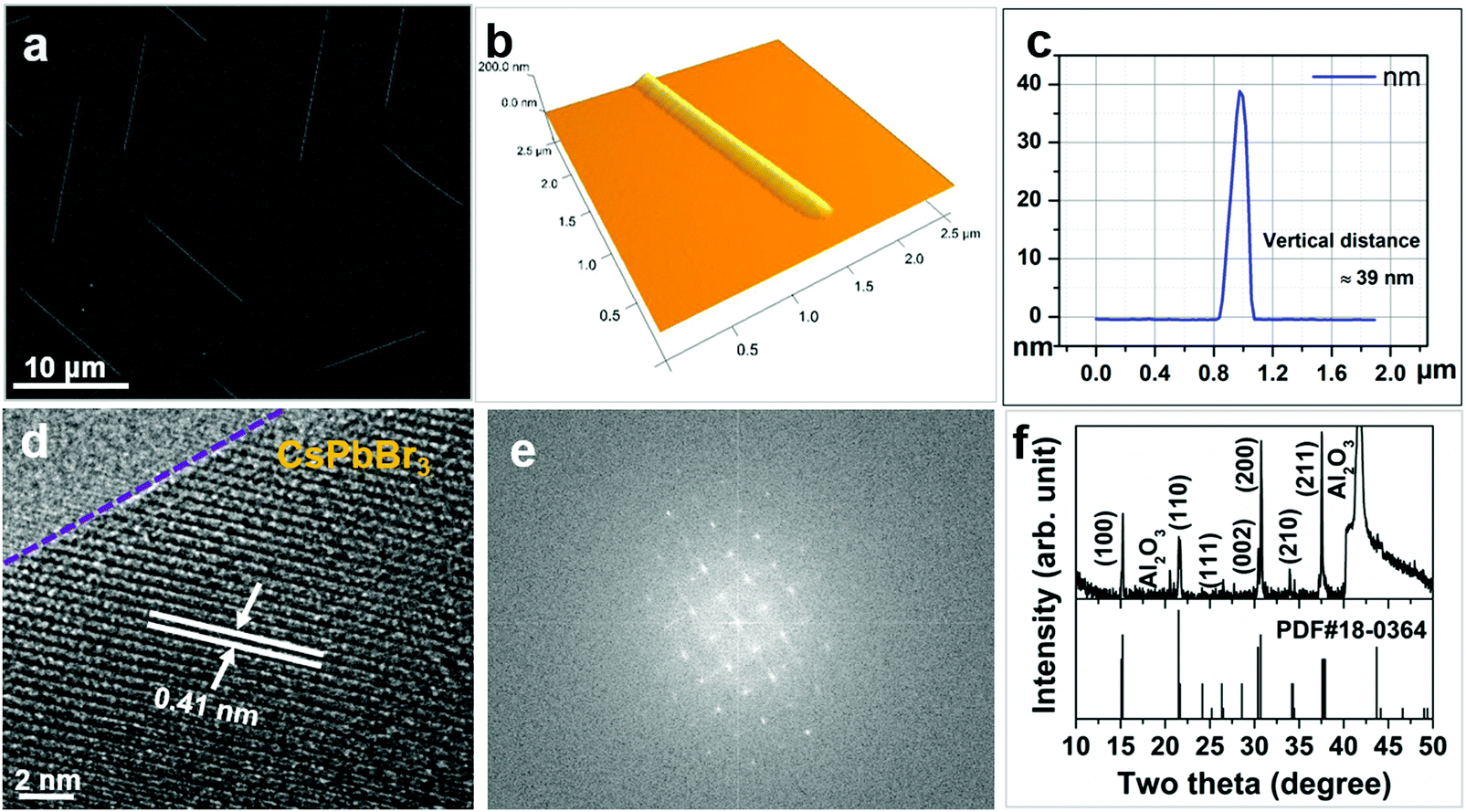 | ||
| Fig. 1 (a) A field emission scanning electron microscopy (FESEM) image of CsPbBr3 NWs grown on c-Al2O3. (b and c) An atomic force microscopy (AFM) image showing triangular morphology and the corresponding line scan showing the height of the nanowire. (d and e) A HRTEM image and the corresponding FFT pattern of a CsPbBr3 NW. (f) An X-ray diffraction pattern from CsPbBr3 NWs grown on c-Al2O3. | ||
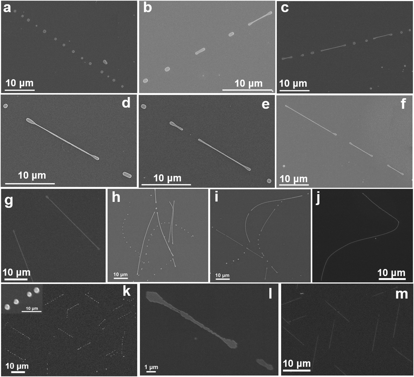 | ||
| Fig. 2 FESEM images at different steps in the NC-CVD growth of CsPbBr3 NWs on: (a–j) amorphous SiO2/Si and (k–m) crystalline c-Al2O3 substrates. (g and j) and (m) show different final shapes of CsPbBr3 NWs on SiO2/Si and Al2O3 substrates, respectively. | ||
Transmission electron microscopy (TEM) and energy dispersive X-ray spectroscopy (EDX) studies confirm that these NWs are single crystalline with the expected 1:1:3 (Cs:Pb:Br) elemental composition. The lattice spacing of d = 0.41 nm is obtained from the high-resolution transmission electron microscopy (HRTEM) image shown in Fig. 1d, which corresponds to the (110) plane of the monoclinic CsPbBr3 crystal phase.16 The monoclinic crystal structure of the CsPbBr3 NWs is further confirmed by the corresponding fast Fourier transform (FFT) of the HRTEM image and the X-ray diffraction pattern shown in Fig. 1e and f, respectively. Note that in the XRD pattern the intensity ratio of the diffraction peaks are different from that of the powder diffraction pattern. This suggests that the growth direction of nanowires was not random. Within the area covered by the X-ray beam, more of the NWs were grown with a preferred (100) direction so that the diffraction peaks from the (100) and (200) planes are stronger. Likewise, microstructural information along with well-defined triangular prismatic morphology was observed for high-quality CsPbCl3 NWs. In this case, a tetragonal crystalline phase was confirmed by both XRD and HRTEM studies (Fig. S4, ESI†), similar to a previous report on the same materials system.16
The chemical compositions and the valence state of different elements were studied by XPS measurements. The binding energies in XPS spectra are calibrated with the C 1s peak at 284.4 eV. The core level spectra of Cs 3d, Pb 4f and Br 3d of the self-assembled all-inorganic CsPbBr3 NWs are shown in Fig. S5 (ESI†). The Cs 3d5/2 peak with binding energy at 724.8 eV shown in Fig. S5b (ESI†) is comparable to that obtained for hybrid halide perovskites and that for all-inorganic CsPbBr3 quantum dots reported earlier.43,44 The peaks with binding energies at 139 and 143.8 eV in Fig. S5c (ESI†) are consistent with values for Pb 4f7/2 and Pb 4f5/2 in PbBr2, respectively. Finally, the peak at binding energy of 74.1 eV can be assigned to Br 3d1/2 which is shown in Fig. S5d (ESI†).14,43–46 Similar XPS survey and core level spectra were also obtained for CsPbCl3 NWs. Composition information obtained from XPS measurements further confirmed values obtained from energy dispersive X-ray spectroscopy (EDS) in the TEM. EDS elemental mappings of CsPbX3 (X = Br, Cl) nanowires reveal that all the component elements are evenly distributed throughout the investigated structures. The corresponding elemental mapping obtained for the representative CsPbX3 (X = Br, Cl) NWs samples are shown in Fig. S6 (ESI†).
2.2 Nanowire formation through vapor phase self-assembly mechanism
A systematic study was performed to understand the mechanism of the NC-CVD growth of IHP NWs. Fig. 2 shows a series of FESEM images of NC-CVD grown CsPbBr3 NWs at different growth stages on both amorphous SiO2 (a–j) and crystalline c-Al2O3 (k–m) substrates. These images reveal that irrespective of the crystallinity of the substrate, NWs were grown via a mechanism involving the nucleation of metal halide particles (Fig. 3a and d) followed by a self-assembly of these particles into longer chains (Fig. 2a–f, h–i and k, l), and finally forming complete nanowires (Fig. 2g, j and m). Note that these features are present in different areas of the sample after a single growth process.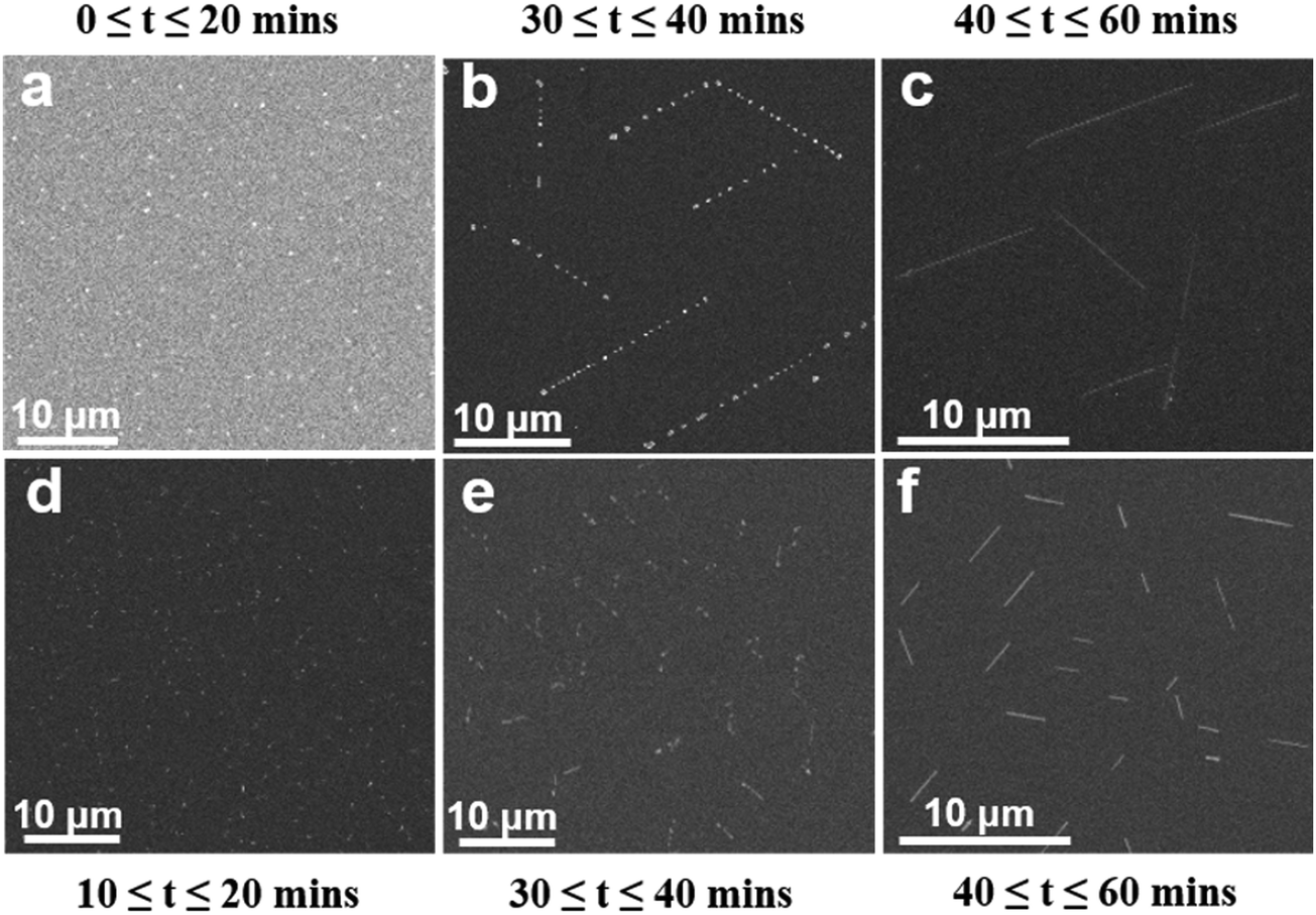 | ||
| Fig. 3 Time evolution of CsPbX3 (X = Br, Cl) perovskite nanowires in NC-CVD growth. (a–c) and (d–f) are the FESEM images of 3 different stages of the time evolution growth of CsPbBr3 and CsPbCl3 perovskite nanowires, respectively. | ||
For a better understanding of the growth mechanism, we performed a series of NC-CVD NW growths for different growth time durations. Fig. 3 shows a series of FESEM images of the growth evolution of CsPbBr3 (Fig. 3a–c) and CsPbCl3 (Fig. 3d–f) NWs on the c-Al2O3 substrate for different growth time durations. The different features obtained at different stages of the NW growth are clearly illustrated in the figure. As soon as the furnace temperature reaches the highest optimized set value, precursor vapors are generated. Vapors are then transported to the downstream CVD zone by a constant flow of the carrier gas. Due to the temperature gradient between centre and the downstream zone of the CVD furnace, condensation of the vapor molecules occurs on the substrate surface.47 Within the first 10–20 min of the growth, this thermal gradient facilitates the nucleation of the CsPbX3 vapor particles onto the substrates.48 As is seen in Fig. 3a and d, within this time frame, random nucleation, and agglomeration of CsPbBr3 and CsPbCl3 particles, respectively, occur on the substrate with ∼200 nm in the particle size.
Prolonged growth duration to 30–40 min results in a reduction in the small halide particle population18 and the growth of individual sphere-like shape particles up to hundreds of nm in size (Fig. 2a, k and 3b, e). Such Ostwald ripening of metal halide nanoparticles arises from more deposited materials as well as mass transfer from smaller neighboring particles, resulting in the observed reduction in the density of smaller particles formed earlier in the growth.49 In addition to the ripening, these halide nanoparticles further reorganize themselves in an energetically favorable way.49,50 The particle rearrangement is found to be strongly dictated by the nature of the substrate. They tend to distribute randomly on an amorphous substrate as seen in Fig. 2a, h and i. On a crystalline c-Al2O3 substrate, however, they follow the crystalline facets forming straight line patterns as shown in Fig. 2k and 3b, e.26,38
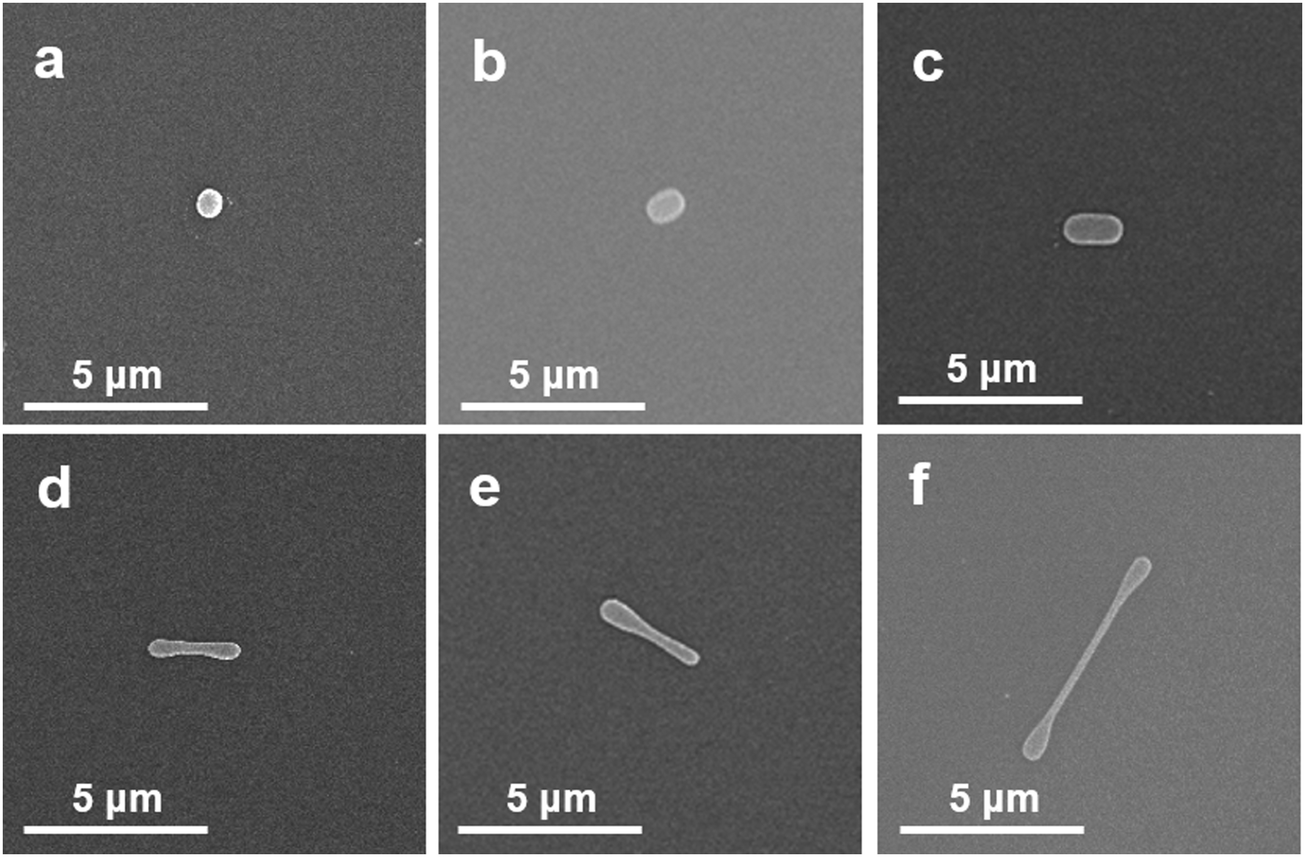
The sphere like halide particles develop into NW structures via a physiological transformation by first attaining stable dumbbell like shapes. These dumbbell-shaped structures then elongate to several microns long and eventually coalesce with their ends meeting, as shown as swollen nodes in Fig. 4b–d. Fig. 4a–h illustrate the formation of NWs from these dumbbell structures at different stages. Note that initially when the ends of several dumbbell shapes meet, the NW is non-uniform in shape showing swollen connection nodes. These swollen parts finally smoothen out through atomic diffusion within the NW and form uniform straight wire on c-Al2O3 (Fig. 4f) and curvy wire on SiO2 substrates (Fig. 4h). NWs with length larger than 10 μm for CsPbBr3 (Fig. 2g, j, m and 3c) and of around 5 μm for CsPbCl3 (Fig. 3f) are eventually formed.
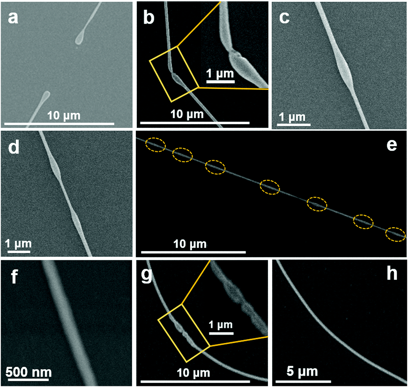 | ||
| Fig. 4 End to end coalescence of dumbbell shaped structures of CsPbBr3 during the formation of complete NWs. (a–c) Different steps in the coalescence of two ends of two dumbbells. (d) Coalescence of 3 dumbbells. (e) Coalescence of multiple dumbbells followed by further transformations through axial elongation and radial contraction. (f) High resolution FESEM image of a CsPbBr3 NW grown on c-Al2O3 substrate. (g and h) Coalescence of curved shapes and formation of smooth-curvy NW on SiO2 substrate. | ||
The transformation of the sphere like halide particles into dumbbell shape can be qualitatively described in terms of a rotating drop model and is illustrated by FESEM images in Fig. 5 for different features observed.51 We first consider a sphere like halide particle as a chargeless liquid drop on the substrate surface at the respective NC-CVD growth atmosphere. The carrier gas flow continuously applies a torque on the metal halide drop which causes them to experience a rotation. When this chargeless drop rotates around its own axis, initially transforming into a capsule like structure as shown in Fig. 5b and c. A further increase in the angular velocity extends it axially to a direction perpendicular to its axis of rotation. If the angular velocity of rotation, Ω (or the corresponding angular momentum) continues to increase and reaches a number less than its critical value, Ω* = Ω′√8T/(ρa)3 (where Ω′ is a dimensionless quantity and is analytically found to be equal to 0.559, and ρ is the density of liquid) the ends of the “capsule” then enlarges and transforms into a dumbbell like structure as seen in Fig. 5d–f.51 The critical angular velocity can be roughly defined as the velocity above which the axisymmetric balance breaks up, resulting in splitting of the capsule. Here, it is important to note that the transformation of the spherical droplet into a “capsule” and, finally, a dumbbell increases the moment of inertia, and hence decreases the angular velocity of the system. This gives the stable ultimate dumbbell shape to the transformed structure.51,52Fig. 5a–f show different shaped structures on SiO2 substrate, illustrating the transformation steps in attaining the stable dumbbell structure. Although the morphologies of the final NWs grown on amorphous and crystalline substrates are different, the initial nucleation of sphere like particles and their subsequent transformation into the dumbbell structures are independent of the substrate (Fig. 2d and l). Note that, all the transformations here are to attain structural stability through surface energy minimization, resulting in the final NW formation.53
 | ||
| Fig. 5 (a–f) Successive transformations of CsPbBr3 single halide particle into a stable dumbbell shape during the growth of single-crystalline halide nanowires by the NC-CVD. | ||
2.3 Correlations of the nanoparticle, dumbbell features to nanowires
The above qualitative model suggests that IHP NWs are formed through the self-assembly of spherical halide particles followed by their subsequent intermediate transformations and coalescence. Here, we provide spectroscopic evidence that at each stage of the NW formation, the different features are composed of the same halide perovskite.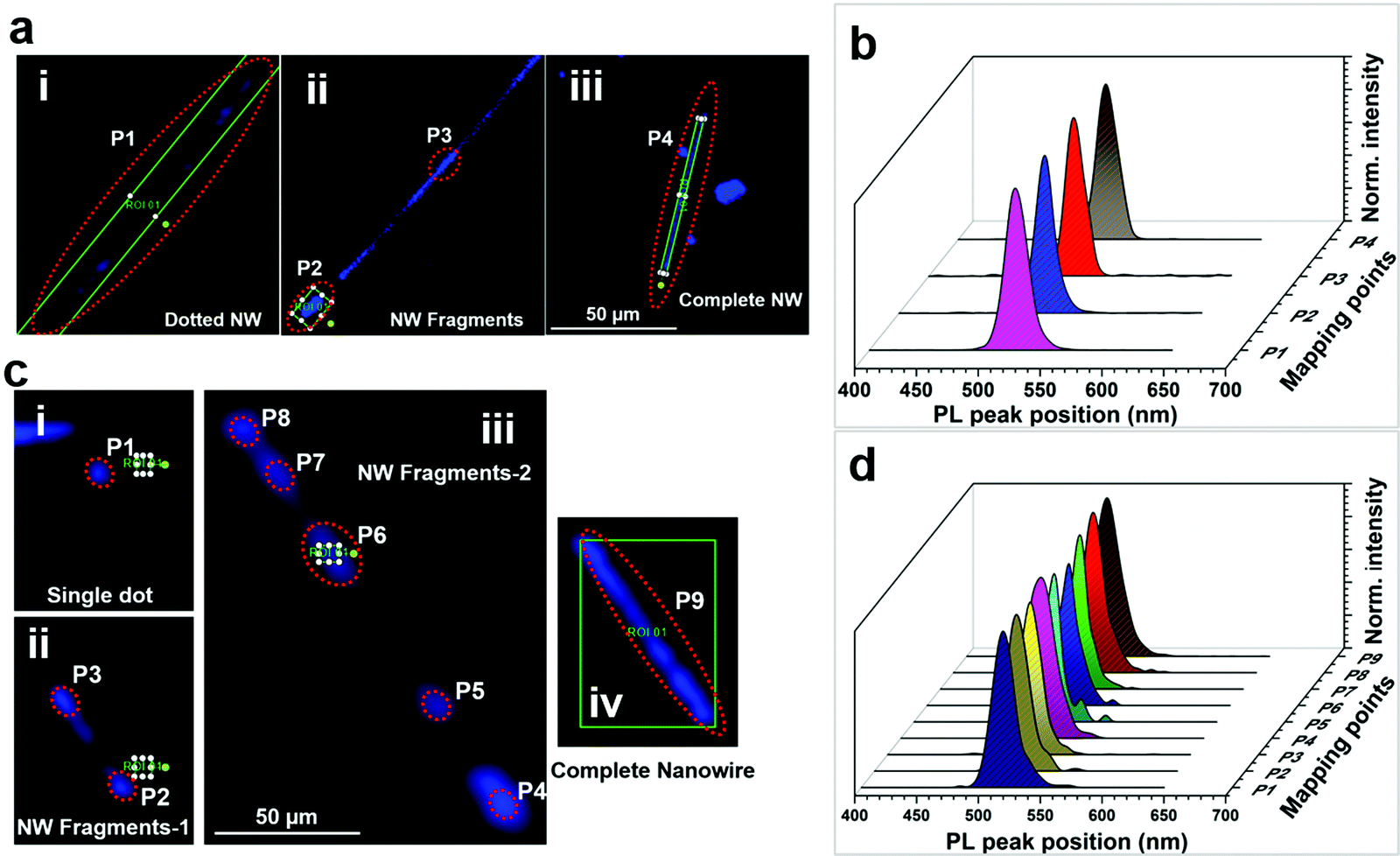 | ||
| Fig. 6 Photoluminescence (PL) mapping and the corresponding PL spectra of CsPbBr3 dot like spherical halide particles, incomplete NWs/NW fragments, and complete NWs grown respectively on (a and b) SiO2/Si- and (c and d) c-Al2O3 substrate. P1 to P9 denote the PL measurement spots on different structures and/or position on the same structures. Color in the PL scanning map does not represent the real emission color. | ||
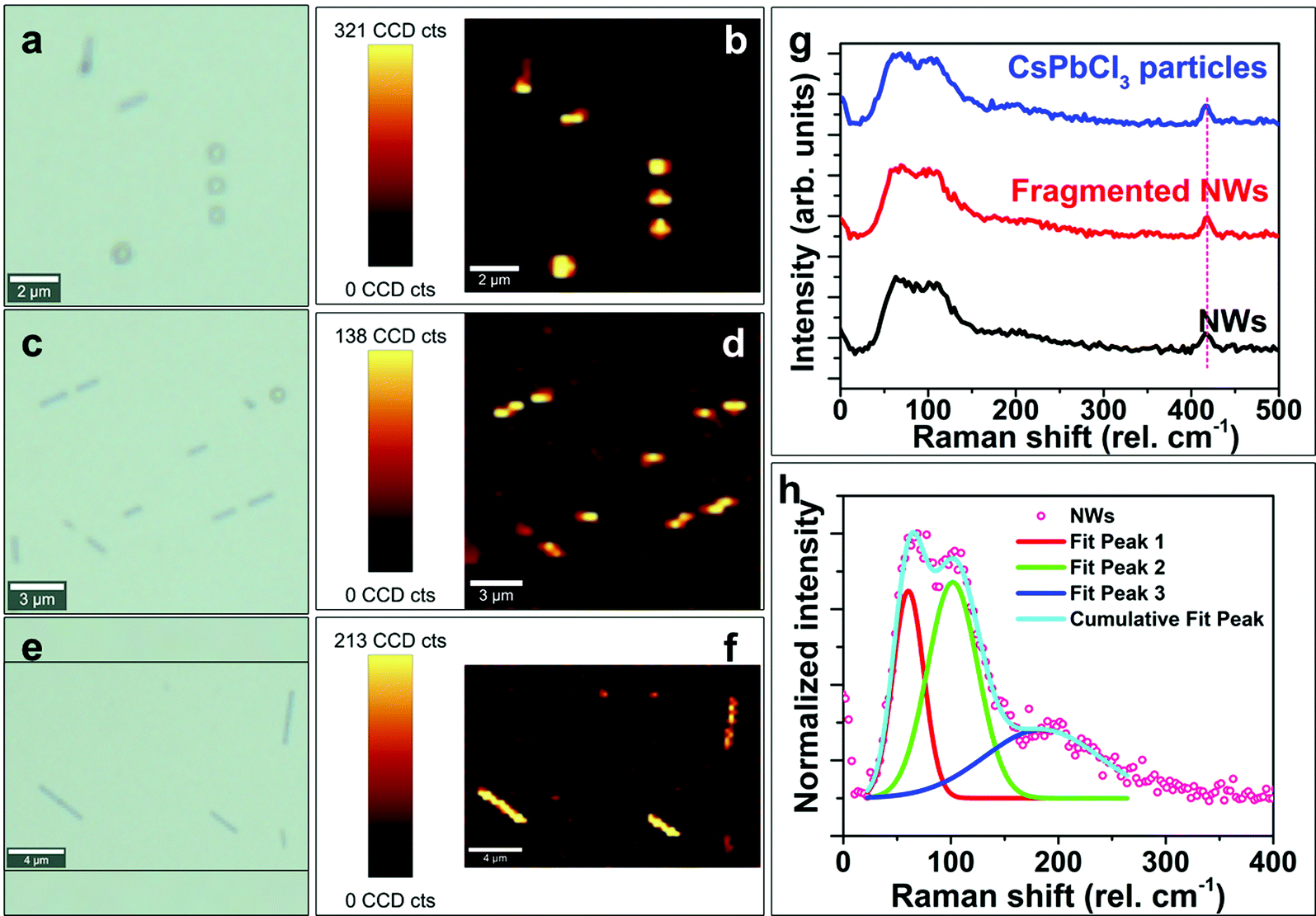 | ||
| Fig. 7 μ-Raman characterization of various morphological features of self-assembled CsPbCl3 halide perovskites. Confocal microscopy images and corresponding μ-Raman mappings of CsPbCl3 – (a and b) dot like spherical halide particles, (c and d) fragmented or incomplete NWs, and (e and f) complete NWs. (g) Raman spectra of three (3) different nano features. (h) Fitted Raman spectrum of CsPbCl3 NWs showing the three transverse optical phonon modes of CsPbCl3. | ||
3 Conclusion
In this work, we report on the non-catalytic chemical vapor deposition (NC-CVD) growth of all-inorganic CsPbX3 (X = Br, Cl) nanowires. In particular, the NW growth mechanism is studied by detailed electron microscopy and other spectroscopic measurements on nanostructures at different stages of the NW growth. A vapor phase self-assembly mechanism is proposed, initiated by the nucleation of nanoparticles, nanoparticles growth followed by structural transformation through axial elongation into nano-capsules and dumbbell structures, and eventually the dumbbells meet and form NWs. While NWs grown on sapphire are aligned with the hexagonal crystal facets, those grown on amorphous SiO2 substrates have both curvy and straight long morphologies with no specific preferred growth direction. Although NWs grown on different substrates have very different morphology, the growth mechanism are found to be independent of the substrate crystallinity. Photoluminescence (PL) mapping and μ-Raman spectroscopy measurements further demonstrate that nanoscale features found on different substrates at different growth stages have similar material properties as the final NWs. We believe that this self-assembly mechanism can be extended to understand nanostructures evolution of other semiconductor materials and to tune their characteristics to enhance their functionalities for novel optoelectronic devices.4 Materials and methods
All chemicals were purchased from Alfa Aesar and Sigma Aldrich and used as received without any further purification. SiO2/Si and c-plane sapphire (c-Al2O3) wafers were cut into small pieces with the lateral dimensions of (2 × 1) cm2 followed by an ultrasonic cleaning in acetone, ethanol and deionized water for 15 minutes each. The as-cleaned pieces of wafers were blown-dried by dry nitrogen and then put into an oven working at a processing temperature of 100 °C for a period of 24 hours.A home-built CVD system consisting of a single-zone horizontal tube furnace, OTF-1200X, Hefei Kejing Materials Technology Co. Ltd, was used to grow the all-inorganic cesium lead halide perovskite, CsPbX3 (X = Br, Cl) nanowires (NWs). The furnace was equipped with a quartz tube having an inner diameter of 2.2 cm and a length of 85 cm. The tube was coupled with a carrier gas inlet, a mass flow controller, a flow meter, and a vacuum pumping system (Fig. S1, ESI†).
A rectangular shape boron nitride boat (2 × 1 × 1) cm3 loaded with CsBr and PbBr2, having a molar weight fraction of 1:1 was placed at the centre of the heating zone of the CVD furnace. A few numbers of cleaned SiO2/Si (c-Al2O3) substrates were put in the downstream side of the heating zone to collect the growth products. After proper sealing, the system was pumped down to a base pressure of ∼≤5.0 mT. High purity Ar (99.99%) with a high flow rate of 100 standard cubic centimetre per minute (sccm) was introduced into the tube for 20 minutes to purge residual air and impurities inside the quartz tube. The flow was then adjusted down to 30 sccm. The desired stable growth pressure of 4.8 T was achieved by adjusting a needle valve placed between the tube and the rotary pump. The furnace was then ramp up (30 °C per min) to the optimized growth temperature of 450 °C. The growth was conducted for another 10–60 min. The furnace was then allowed to cool down naturally. As soon as the furnace temperature reached the room temperature, samples were removed.
It was found that except for the variation in growth time (∼20–60 min), a small variation in the growth temperature (420–450 °C) did not influence the growth. The growth of CsPbBr3 NWs was found to be initiated at the beginning of this time range while at the end, they transformed themselves into complete NWs through the self-assembly mechanism. Accordingly, this time range is referred to as the evolution time of CsPbBr3 NWs growth. The similar growth procedure was adopted for growing CsPbCl3 NWs except for replacing the precursor materials by CsCl and PbCl2 in the precursor mixture. For self-assembled CsPbCl3 NWs, the growth temperature was found to be in the range between 450–500 °C while the evolution time range was similar to that of CsPbBr3 NWs growth.
4.1 Material characterizations
Morphology of CsPbX3 NWs were studied chronologically by optical microscope (Olympus), field emission scanning electron microscope (FESEM, JEOL JSM-6335F) and atomic force microscope (AFM) (di MultiModeV (Veeco)) facilities. Crystallographic data were collected from the X-ray diffractometer, Bruker D2 phaser. TEM micrographs and the elemental maps were obtained using a Libra200 microscope operated at 200 kV and the EDS facility coupled with the TEM, respectively. The chemical compositions and the valence state of different elements were studied by XPS measurements. Optical properties e.g., photoluminescence (PL) and absorbance were studied respectively by a home-made PL setup and a UV-vis-NIR spectrophotometry setup (MProbe, Thin Film Measurement System (Semiconsoft, Inc.)). A continuous wave (cw) 320 nm He-Cd laser excitation was used for the steady state PL measurements. A WITec alpha300 R μ-Raman setup was also used to perform μ-Raman mapping to study the structural uniformity of the halide alloy materials. Fluorescence images were obtained from a Nikon ECLIPSE TS 100 microscopy.Data availability
Data are available from the corresponding author only upon request.Conflicts of interest
There are no conflicts to declare.Acknowledgements
This work was supported by CityU SGP (No. 9380076). JH acknowledges the support of the General Research Fund (CityU 11306520) of Research Grants Council of Hong Kong SAR.References
- Y. Gao, L. Zhao, Q. Shang, Y. Zhong, Z. Liu, J. Chen, Z. Zhang, J. Shi, W. Du, Y. Zhang, S. Chen, P. Gao, X. Liu, X. Wang and Q. Zhang, Adv. Mater., 2018, 30, 1801805 CrossRef.
- J. Chen, Y. Fu, L. Samad, L. Dang, Y. Zhao, S. Shen, L. Guo and S. Jin, Nano Lett., 2020, 17, 460–466 CrossRef.
- K. Hong, Q. Van Le, S. Y. Kim and H. W. Jang, J. Mater. Chem. C, 2018, 6, 2189–2209 RSC.
- Y. Fu, H. Zhu, J. Chen, M. P. Hautzinger, X. Y. Zhu and S. Jin, Nat. Rev. Mater., 2019, 4, 169–188 CrossRef CAS.
- M. Lai, Q. Kong, C. G. Bischak, Y. Yu, L. Dou, S. W. Eaton, N. S. Ginsberg and P. Yang, Nano Res., 2017, 10, 1107–1114 CrossRef CAS.
- J. Du, J. Xing, C. Ge, H. Liu, P. Liu, H. Hao, J. Dong, Z. Zheng and H. Gao, J. Phys. D: Appl. Phys., 2016, 49, 425105 Search PubMed.
- J. J. Zhang, G. Katsaros, F. Montalenti, D. Scopece, R. O. Rezaev, C. Mickel, B. Rellinghaus, L. Miglio, S. De Franceschi, A. Rastelli and O. G. Schmidt, Phys. Rev. Lett., 2012, 109, 085502 CrossRef CAS.
- Y. Xia, P. Yang, Y. Sun, Y. Wu, B. Mayers, B. Gates, Y. Yin, F. Kim and H. Yan, Adv. Mater., 2003, 15, 353–389 CrossRef CAS.
- R. G. Hobbs, S. Barth, N. Petkov, M. Zirngast, C. Marschner, M. A. Morris and J. D. Holmes, J. Am. Chem. Soc., 2010, 132, 13742–13749 CrossRef CAS.
- P. Gao, A. R. Bin Mohd Yusoff and M. K. Nazeeruddin, Nat. Commun., 2018, 9, 5028 CrossRef.
- Best research-cell efficiencies (NREL, accessed 22 December 2020); https://www.nrel.gov/pv/assets/pdfs/best-research-cell-efficiencies.20200925.pdf.
- Y. Fu, H. Zhu, C. C. Stoumpos, Q. Ding, J. Wang, M. G. Kanatzidis, X. Zhu and S. Jin, ACS Nano, 2016, 10, 7963–7972 CrossRef CAS.
- K. Park, J. W. Lee, J. D. Kim, N. S. Han, D. M. Jang, S. Jeong, J. Park and J. K. Song, J. Phys. Chem. Lett., 2016, 7, 3703–3710 CrossRef CAS.
- Y. Li, Z. Shi, L. Lei, Z. Ma, F. Zhang, S. Li, D. Wu, T. Xu, X. Li, C. Shan and G. Du, ACS Photonics, 2018, 5, 2524–2532 CrossRef CAS.
- Y. Wang, M. I. Dar, L. K. Ono, T. Zhang, M. Kan, Y. Li, L. Zhang, X. Wang, Y. Yang, X. Gao, Y. Qi, M. Grätzel and Y. Zhao, Science, 2019, 365, 591–595 CrossRef CAS.
- H. Zhou, S. Yuan, X. Wang, T. Xu, X. Wang, H. Li, W. Zheng, P. Fan, Y. Li, L. Sun and A. Pan, ACS Nano, 2017, 11, 1189–1195 CrossRef CAS.
- L. Huang, Q. Gao, L. D. Sun, H. Dong, S. Shi, T. Cai, Q. Liao and C. H. Yan, Adv. Mater., 2018, 30, 1800596 CrossRef.
- D. Zhang, S. W. Eaton, Y. Yu, L. Dou and P. Yang, J. Am. Chem. Soc., 2015, 137, 9230–9233 CrossRef CAS.
- T. Yang, Y. Zheng, Z. Du, W. Liu, Z. Yang, F. Gao, L. Wang, K. C. Chou, X. Hou and W. Yang, ACS Nano, 2018, 12, 1611–1617 CrossRef CAS.
- Y. Zhang, H. Zhu, J. Zheng, G. Chai, Z. Song, Y. Chen, Y. Liu, S. He, Y. Shi, Y. Tang, M. Wang, W. Liu, L. Jiang and S. Ruan, J. Phys. Chem. C, 2019, 123, 4502–4511 CrossRef CAS.
- S. Yakunin, L. Protesescu, F. Krieg, M. I. Bodnarchuk, G. Nedelcu, M. Humer, G. De Luca, M. Fiebig, W. Heiss and M. V. Kovalenko, Nat. Commun., 2015, 6, 8056 CrossRef CAS.
- G. Tong, H. Li, D. Li, Z. Zhu, E. Xu, G. Li, L. Yu, J. Xu and Y. Jiang, Small, 2018, 14, 1702523 CrossRef.
- M. K. Hossain, P. Guo, W. Qarony, Y. H. Tsang, C. Liu, S. W. Tsang, J. C. Ho and K. M. Yu, Nano Res., 2020, 13, 2939–2949 CrossRef CAS.
- P. Guo, M. K. Hossain, X. Shen, H. Sun, W. Yang, C. Liu, C. Y. Ho, C. K. Kwok, S. Tsang, Y. Luo, J. C. Ho and K. M. Yu, Adv. Opt. Mater., 2018, 6, 1700993 CrossRef.
- D. Zhang, Y. Yu, Y. Bekenstein, A. B. Wong, A. P. Alivisatos and P. Yang, J. Am. Chem. Soc., 2016, 138, 13155–13158 CrossRef CAS.
- E. Oksenberg, E. Sanders, R. Popovitz-Biro, L. Houben and E. Joselevich, Nano Lett., 2018, 18, 424–433 CrossRef CAS.
- Y. Meng, C. Lan, F. Li, S. Yip, R. Wei, X. Kang, X. Bu, R. Dong, H. Zhang and J. C. Ho, ACS Nano, 2019, 13, 6060–6070 CrossRef CAS.
- Q. Shang, M. Li, L. Zhao, D. Chen, S. Zhang, S. Chen, P. Gao, C. Shen, J. Xing, G. Xing, B. Shen, X. Liu and Q. Zhang, Nano Lett., 2020, 20, 6636–6643 CrossRef CAS.
- Y. Gao, L. Zhao, Q. Shang, C. Li, Z. Liu, Q. Li, X. Wang and Q. Zhang, J. Semicond., 2019, 40, 052201 CrossRef CAS.
- Z. Liu, Q. Shang, C. Li, L. Zhao, Y. Gao, Q. Li, J. Chen, S. Zhang, X. Liu, Y. Fu and Q. Zhang, Appl. Phys. Lett., 2019, 114, 101902 CrossRef.
- D. Pan, Y. Fu, J. Chen, K. J. Czech, J. C. Wright and S. Jin, Nano Lett., 2018, 18, 1807–1813 CrossRef CAS.
- J. K. Meyers, S. Kim, D. J. Hill, E. E. M. Cating, L. J. Williams, A. S. Kumbhar, J. R. McBride, J. M. Papanikolas and J. F. Cahoon, Nano Lett., 2017, 17, 7561–7568 CrossRef CAS.
- Y. Wang, X. Guan, D. Li, H. Cheng, X. Duan, Z. Lin and X. Duan, Nano Res., 2017, 10, 1223–1233 CrossRef CAS.
- R. Chen, T. T. D. Tran, K. W. Ng, W. S. Ko, L. C. Chuang, F. G. Sedgwick and C. Chang-Hasnain, Nat. Photonics, 2011, 5, 170–175 CrossRef CAS.
- J. L. Lensch-Falk, E. R. Hemesath, F. J. Lopez and L. J. Lauhon, J. Am. Chem. Soc., 2007, 129, 10670–10671 CrossRef CAS.
- L. V. Podrezova, S. Porro, V. Cauda, M. Fontana and G. Cicero, Appl. Phys. A: Mater. Sci. Process., 2013, 113, 623–632 CrossRef CAS.
- C. Li, L. Zhao, H. Fan, Q. Shang, W. Du, J. Shi, Y. Zhao, X. Liu and Q. Zhang, Adv. Opt. Mater., 2020, 8, 2000743 CrossRef CAS.
- Y. Wang, X. Sun, R. Shivanna, Y. Yang, Z. Chen, Y. Guo, G. C. Wang, E. Wertz, F. Deschler, Z. Cai, H. Zhou, T. M. Lu and J. Shi, Nano Lett., 2016, 16, 7974–7981 CrossRef CAS.
- M. Shoaib, X. Zhang, X. Wang, H. Zhou, T. Xu, X. Wang, X. Hu, H. Liu, X. Fan, W. Zheng, T. Yang, S. Yang, Q. Zhang, X. Zhu, L. Sun and A. Pan, J. Am. Chem. Soc., 2017, 139, 15592–15595 CrossRef CAS.
- Q. Shang, C. Li, S. Zhang, Y. Liang, Z. Liu, X. Liu and Q. Zhang, Nano Lett., 2020, 20, 1023–1032 CrossRef CAS.
- X. Wang, M. Shoaib, X. Wang, X. Zhang, M. He, Z. Luo, W. Zheng, H. Li, T. Yang, X. Zhu, L. Ma and A. Pan, ACS Nano, 2018, 12, 6170–6178 CrossRef CAS.
- P. X. Gao and Z. L. Wang, J. Am. Chem. Soc., 2003, 125, 11299–11305 Search PubMed.
- M. Deepa, M. Salado, L. Calio, S. Kazim, S. M. Shivaprasad and S. Ahmad, Phys. Chem. Chem. Phys., 2017, 19, 4069–4077 RSC.
- H. Chen, A. Guo, J. Zhu, L. Cheng and Q. Wang, Appl. Surf. Sci., 2019, 465, 656–664 CrossRef CAS.
- C. Yuan, X. Li, S. Semin, Y. Feng, T. Rasing and J. Xu, Nano Lett., 2018, 18, 5411–5417 CrossRef CAS.
- M. Zhang, Z. Q. Tian, D. L. Zhu, H. He, S. W. Guo, Z. L. Chen and D. W. Pang, New J. Chem., 2018, 42, 9496–9500 RSC.
- S. Xu, P. E. Laibinis and G. Y. Liu, J. Am. Chem. Soc., 1998, 120, 9356–9361 CrossRef CAS.
- H. Roder, E. Hahn, H. Brune, J. B. Ie and K. Kern, Nature, 1993, 366, 141–143 CrossRef.
- H. J. Lee, U. J. Yang, K. N. Kim, S. Park, K. H. Kil, J. S. Kim, A. M. Wodtke, W. J. Choi, M. H. Kim and J. M. Baik, Nano Lett., 2019, 19, 4306–4313 CrossRef CAS.
- M. Zeng, L. Wang, J. Liu, T. Zhang, H. Xue, Y. Xiao, Z. Qin and L. Fu, J. Am. Chem. Soc., 2016, 138, 7812–7815 CrossRef CAS.
- L. Liao and R. J. A. Hill, Phys. Rev. Lett., 2017, 119, 114501 CrossRef CAS.
- J. T. Holgate and M. Coppins, Phys. Fluids, 2018, 30, 064107 CrossRef.
- Y. W. Jun, M. F. Casula, J. H. Sim, S. Y. Kim, J. Cheon and A. P. Alivisatos, J. Am. Chem. Soc., 2003, 125, 15981–15985 CrossRef CAS.
- M. Liao, B. Shan and M. Li, J. Phys. Chem. Lett., 2019, 10, 1217–1225 CrossRef CAS.
- D. M. Calistru, L. Mihut, S. Lefrant and I. Baltog, J. Appl. Phys., 1997, 82, 5391–5395 CrossRef CAS.
Footnote |
| † Electronic supplementary information (ESI) available. See DOI: 10.1039/d1tc00077b |
| This journal is © The Royal Society of Chemistry 2021 |