
 Open Access Article
 This Open Access Article is licensed under a
 Creative Commons Attribution 3.0 Unported Licence
Improved performance of perovskite light-emitting diodes with a NaCl doped PEDOT:PSS hole transport layer†
Xiaokun
Huang
abc,
Rainer
Bäuerle
ad,
Felix
Scherz
ac,
Jean-Nicolas
Tisserant
a,
Wolfgang
Kowalsky
abc,
Robert
Lovrinčić
abe and
Gerardo
Hernandez-Sosa
 *afg
*afg
aInnovationLab, Heidelberg 69115, Germany. E-mail: gerardo.sosa@kit.edu
bInstitute for High-Frequency Technology, Braunschweig Technical University, Braunschweig 38106, Germany
cKirchhoff-Institut für Physik, Ruprecht-Karls-Universität Heidelberg, Heidelberg 69120, Germany
dOrganisch-Chemisches Institut, Ruprecht-Karls-Universität Heidelberg, Heidelberg 69120, Germany
eTrinamiX GmbH, Ludwigshafen 67063, Germany
fInstitute of Microstructure Technology, Karlsruhe Institute of Technology, Eggenstein-Leopoldshafen 76344, Germany
gLight Technology Institute, Karlsruhe Institute of Technology, Karlsruhe 76131, Germany
First published on 9th March 2021
Abstract
We demonstrate a simple and effective way to enhance the performance of perovskite light-emitting diodes (PeLEDs) by utilizing an alkali halide doped PEDOT:PSS as the hole transport layer (HTL). The alkali halide (NaCl) doping helped the growth of the quasi-2D perovskite phases on top of the PEDOT:PSS, it also significantly reduced the exciton quenching in PEDOT:PSS based PeLEDs. More importantly, the doping reduced the work function of the PEDOT:PSS surface, which appropriately modulated the hole injection leading to improved charge balance. This helps to control the recombination zone inside the thin perovskite emitting layer (∼10 nm). The optimized blue-green PeLEDs with the NaCl doped PEDOT:PSS HTL showed a maximum luminance of 1487 cd m−2, current efficiency of 2.16 cd A−1 with a low turn-on voltage of 3.0 V, which are 217% and 567% higher than the PeLEDs with the pristine PEDOT:PSS layer (turn-on voltage: 3.3 V), respectively.
Owing to their excellent properties such as simple solution-based fabrication process, high photoluminescence quantum yield (PLQY), tunable spectral bandgaps, narrow emission bandwidths, and superior carrier transport properties,1–4 metal halide perovskite (MHP) light-emitting diodes (PeLEDs) have attracted great research interest in recent years. Tremendous progress has been made in this field since the first development of room temperature operable PeLEDs in 2014,5 the external quantum efficiencies (EQE) of red and green PeLEDs have both reached more than 20%,6,7 approaching theoretical limits of conversion efficiency.8 However, the performance of blue PeLEDs is still lagging behind. The intrinsic wide-bandgap nature and difficult charge injection from charge transport layers cause energy down-conversion and severe nonradiative recombination, making the realization of efficient blue PeLEDs a challenge. This impedes the future industrialization process of PeLEDs as blue is one of the three primary colors needed in displays and white lighting applications.9 Therefore, it is of significant importance to select suitable charge transport materials for efficient charge injection into blue perovskite emitter.
Typically, the structures of PeLEDs stem from those of organic light-emitting diodes (OLEDs) or perovskite solar cells where the perovskite emitting layer (EML) is sandwiched between an electron transport layer (ETL) and a hole transport layer (HTL). For HTL, poly(3,4-ethylenedioxythiophene): poly(styrene sulfonate) (PEDOT:PSS) is the most commonly used material due to its easy solution-based fabrication process, high transmittance, and high hole mobility (0.0128 cm2 V−1 s−1).10 Nevertheless, the work function of PEDOT:PSS (ca. 5.2 eV) is much lower than the ionization potential (IP) of MHPs (5.6–5.7 eV), leading to large barriers for hole injection as well as substantial nonradiative decay at the interface. This is even worse for blue-emitting MHPs as the IP can be as high as 6 eV.11,12 It has also been reported that the positively charged PEDOT chain interacts strongly with the negatively charged Br− of the overlying MHP layer, further quenching its light emission.13,14 Furthermore, polycrystalline MHP films spin-coated on the surface of conventional PEDOT:PSS typically present poor morphology, resulting in huge leakage current and degraded device performance,15,16 which is another drawback impeding the use of PEDOT:PSS as an ideal HTL in PeLEDs. To solve this problem, there are already a variety of strategies to improve the interface of PEDOT:PSS and perovskite EML such as adding a higher work function interlayer,17 adding additives in PEDOT:PSS18 or solvent treatments.19 In the field of blue PeLEDs, for example, Hoye et al. modified the PEDOT:PSS and the EML interface with a poly(triarylamine) interlayer and found the EQEs increased by almost two orders of magnitude for both a blue and sky-blue PeLEDs;20 Congreve et al. constructed a bilayer HTL blended with Nafion perfluorinated ionomer (PFI) on top of PEDOT:PSS, which causes a band bending of HTL to modify and induce well-matched energy levels with perovskite nanocrystals, they found this new structure enables efficient devices across the entire blue to green portion of the spectrum;12 Li et al. and Tang et al. replaced the conventional PEDOT:PSS(AI 4083) with PEDOT:PSS(CH 8000) to serve as HTL, it has a deeper work function of ∼5.2 eV but lower hole conductivity, they both achieved enhanced device performance.21,22 Above all, previous work aimed at increasing the work function of ITO/PEDOT:PSS electrode to better match the energy level of perovskite EML thus promoting hole injection as well as minimizing non-radiative losses and charge quenching.
In this work, we improved the HTL/EML interface by a facile method of NaCl doping into PEDOT:PSS solution (abbreviated as PEDOT-Na). We found a significant enhancement of the performance of blue-green PeLEDs with NaCl addition. The improvement originates not only from the increased conductivity of PEDOT:PSS via doping, but also from the precipitation of NaCl on top of PEDOT:PSS which favor the growth of the quasi-2D perovskite layer and reduce the exciton quenching at the interface. Interestingly, in contrast to previous treatments, the surface work function of PEDOT:PSS was reduced by almost 0.6 eV with NaCl doping, which appropriately modulates the injected hole carriers to reach an improved charge balance in our devices.
The alkali halide NaCl has been utilized in the past as a defect passivation layer on ETL and as an additive to control the morphology of the perovskite films.23,24 Besides, NaCl doping in HTLs has proven to create large improvements in the power conversion efficiency (PCE) of perovskite solar cells.25,26 Here, we investigated for the first time the effect of NaCl doping and its implementation in perovskite light-emitting diodes. We followed the method developed by the group of Jin et al.27 for the fabrication of perovskite EML. In their work, a structure of quantum-confined perovskite nanoparticles was found to be embedded within energy coupled quasi-2D phases with higher bandgaps, which give unique blue electroluminescence. The device structure is shown in Fig. 1(a), where TPBi was used as the ETL and LiF/Al served as the top electrode as usual.
 | ||
| Fig. 1 Characteristics of blue-green PeLEDs with different concentrations of NaCl doping. (a) device structure, (b) current density–luminance–voltage characteristics, (c) current efficiency vs. voltage curves, (d) efficacy vs. voltage curves, (e) operational lifetime carried out at a constant current of 7.7 mA, and (f) electroluminescence spectra under the bias of 4 V. Inset are the representative photographs of the electroluminescence of the corresponding devices. | ||
Fig. 1(b) shows the current density–luminance–voltage curves (LIV) of our PeLEDs. The basic device with the pure PEDOT:PSS film showed poor performance with a maximum luminance of 433 cd m−2 (at 6.2 V). In contrast, the optimized PeLEDs with the PEDOT-Na (10 mg mL−1) layer exhibited a significantly improved maximum luminance of 1487 cd m−2 (at 5 V), it also showed a reduced turn-on voltage (determined as the driving voltage at ∼1 cd m−2) of 3.01 V compared to 3.42 V for the PEDOT:PSS based PeLEDs. Furthermore, the addition of NaCl yielded improved current efficiency (CE) and luminance efficacy (LE) as it can be observed in Fig. 1(c and d). The CE and LE of the PeLEDs gradually increased with increasing the NaCl doping concentration to 10 mg mL−1, and then started to decrease at higher concentrations. The statistical analysis of the electroluminescence performance of devices with different NaCl doping concentrations is summarized in Table 1. The corresponding histograms shown in Fig. S1 (ESI†) indicate an overall enhancement of the performance with all utilized NaCl doping concentrations. The device lifetime was also checked. As seen in Fig. 1(e), the best device based on PEDOT-Na (5 mg mL−1) HTL gives the T50 of 420 s, a nearly three folds increase compared to the device with the original PEDOT:PSS layer (106 s). The electroluminescence (EL) spectra are presented in Fig. 1(f), all the devices showed sharp cyan color emission with a single peak centered at ∼505 nm, although there was a slight redshift for PEDOT:PSS based PeLEDs (508 nm) (Fig. S2, ESI†). Fig. S3 (ESI†) shows that the calculated CIE coordinates of the device emission are in the blue-green region. For the most efficient device (10 mg mL−1), the coordinates are located in (0.057, 0.63) (Table S1, ESI†). Also, much brighter emission was observed for the device with PEDOT-Na (10 mg mL−1) HTL from the photographs shown in the inset of Fig. 1(f), consistent with the former observations. Interestingly, there are plenty of “emission boundaries” clearly visible in the device with PEDOT-Na (30 mg mL−1) HTL, which further stimulated us to investigate the underlying mechanisms of the improvement originated from the PEDOT-Na HTL.
| Luminance [cd m−2] | Current efficiency [cd A−1] | Efficacy [lm W−1] | Turn-on voltage [V] | |
|---|---|---|---|---|
| PEDOT | 683.9/398 ± 198.2 | 0.38/0.27 ± 0.08 | 0.26/0.16 ± 0.06 | 3.31/3.57 ± 0.32 |
| PEDOT-Na (5 mg mL−1) | 1366.2/1050.2 ± 205.3 | 2.0/1.26 ± 0.44 | 1.62/0.95 ± 0.39 | 3.0/3.07 ± 0.05 |
| PEDOT-Na (10 mg mL−1) | 1486.9/1303.5 ± 165.4 | 2.16/1.53 ± 0.42 | 1.74/1.13 ± 0.39 | 3.01/3.15 ± 0.09 |
| PEDOT-Na (15 mg mL−1) | 1525.1/1335.5 ± 169.1 | 1.40/1.21 ± 0.20 | 1.0/0.84 ± 0.17 | 3.05/3.11 ± 0.05 |
| PEDOT-Na (30 mg mL−1) | 769.2/535.1 ± 168.7 | 0.79/0.56 ± 0.20 | 0.58/0.40 ± 0.15 | 3.05/3.14 ± 0.09 |
We first studied the morphologies of the PEDOT:PSS layer with and without NaCl doping and found a strong difference in the morphology of the PEDOT:PSS layer upon addition of NaCl. As is shown in the AFM images of Fig. 2(a), the pure PEDOT:PSS layer exhibits a smooth surface with root-mean-square (RMS) of 1.9 nm. However, small aggregates were distributed on top of the PEDOT:PSS surface when 5 mg mL−1 NaCl was added (Fig. 2(b)). More aggregates appeared when the NaCl doping concentration was increased to 10 mg mL−1 as shown in Fig. 2(c). The increasing number of NaCl aggregates then gradually connected to form dendritic structures as the doping concentration was further increased to 15 and 30 mg mL−1, respectively (Fig. 2(d) and (e)). At the same time, the surface roughness also exhibits a dramatic increase as the RMS value for 5 mg mL−1 NaCl doping is 30 nm, and ∼50 nm for 30 mg mL−1. These changes in the morphology of PEDOT:PSS with NaCl addition were also confirmed by optical microscopy images shown in Fig. S4 (ESI†), in which it is visible that the precipitated aggregates gradually formed a thin buffer layer on top of PEDOT:PSS. In particular, it can be seen that plenty of cracks appeared in the buffer layer on top of the PEDOT:PSS film when adding 30 mg mL−1 of NaCl (Fig. S4(e), ESI†). These structures resembled the “emission boundaries” seen from the EL photograph in Fig. 1(f), indicating that the morphology of the HTL indeed plays a role in the emission of the final device.
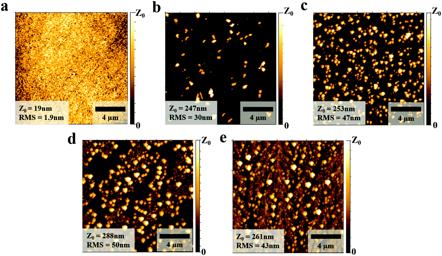 | ||
| Fig. 2 The AFM images of the PEDOT:PSS films (a), and with NaCl doping of different concentrations (b) 5 mg mL−1, (c) 10 mg mL−1, (d) 15 mg mL−1, (e) 30 mg mL−1. | ||
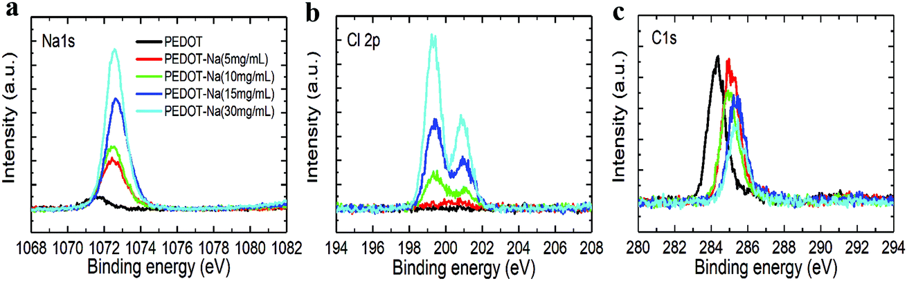
The morphology change was then further corroborated by X-ray photoemission spectroscopy (XPS) measurement, which is a very sensitive method to characterize the surface composition. As depicted in Fig. 3, we observed increasing sodium Na 1s peaks (binding energy 1073 eV) and chloride Cl 2p peaks (binding energy 198 and 201 eV) with increasing NaCl content in the PEDOT:PSS layer, while the Carbon C 1s peaks (binding energy 285 eV) solely associated with the PEDOT:PSS layer decreased. This observation can be explained by the increased coverage of the surface by NaCl (Fig. 2).28 We note the C 1S peaks in Fig. 3(c) exhibited a slight blue shift with NaCl doping. The same trend was also found in the sulfur S 2p peaks shown in Fig. S5 (ESI†), where the peaks between 166 and 172 eV can be assigned to sulfur atoms of PSS while the signals in the range of 162–166 eV correspond to the sulfur atoms of PEDOT.29 Such peak shifts imply that the chemical environment of PEDOT has been changed with NaCl addition,25,30 the incorporated Na+ would bound to the PSS−, resulting in phase separation between insulating PSS and conducting PEDOT chains. Therefore, better charge hopping between conductive PEDOT will occur, which is then correlated to the two-fold increase in conductivity of PEDOT:PSS as shown in Table 2 and Fig. S6(a) (ESI†).
 | ||
| Fig. 3 X-ray photoemission spectroscopy of the PEDOT:PSS films with different concentrations of NaCl doping. | ||
| NaCl/mg mL−1 | 0 | 5 | 10 | 15 | 30 |
|---|---|---|---|---|---|
| Conductivity (S m−1) | 0.022 ± 0.017 | 0.025 ± 0.010 | 0.032 ± 0.004 | 0.041 ± 0.009 | 0.015 ± 0.010 |
| WF(XPS) (eV) | 4.97 ± 0.02 | 4.38 ± 0.02 | 4.38 ± 0.02 | 4.39 ± 0.02 | 4.40 ± 0.02 |
| WF(KP) (eV) | 4.91 ± 0.08 | 4.51 ± 0.03 | 4.54 ± 0.06 | 4.52 ± 0.04 | 4.55 ± 0.06 |
The observed improvement is more likely originated from the improved optoelectronic properties of the perovskite EML and interface to PEDOT:PSS after the incorporation of NaCl. To investigate the impact of NaCl doping on the quality of perovskite film, quasi-2D films (abbreviated as PEABr1.25(Cs0.7FA0.3PbBr3)) were fabricated on PEDOT:PSS and doped PEDOT:PSS substrates via spin-coating. As illustrated in Fig. S7 (ESI†), all the films show a low RMS surface roughness of below 4 nm with small and uniform grains, in good agreement with the reported nanocrystal-like pinhole-free perovskite layer obtained through the one-step method.27 However, we do find that the dendritic structures that were visible within the PEDOT:PSS layer (Fig. 2) are also visible in the AFM images of the perovskite films (Fig. S7(d and e), ESI†), suggesting a templating effect on the perovskite layer. The UV-Vis absorption spectra of perovskite films processed on top of the PEDOT-Na films are shown in Fig. 4(a). The films showed distinct exciton absorption peaks at 403, 432, and 461 nm, which are associated with the n = 1, n = 2, and n = 3 layered perovskites, respectively. Nevertheless, the multiple emission peaks associated with these low-n phases are barely visible when the quasi-2D perovskite films are grown on the pristine PEDOT:PSS layer. It is known that the growth of layered perovskites with the large-size capping cation is very sensitive to the morphology and chemical composition of the underlying substrate.31–33 We believe that the NaCl aggregates forming in and protruding out of the PEDOT:PSS surface (Fig. 2) increase the interface area between the PEDOT:PSS layer and the perovskite film. These aggregates might serve to seed the growth of perovskite crystals and increase the number of low-n phases with large exciton binding energy. We note some of these NaCl aggregates would be dissolved in the DMSO solvent during the perovskite deposition process (Fig. S8, ESI†). However, previous work on the use of NaCl as an additive in the perovskite precursor solution showed no effect on the optoelectronic properties of perovskite film.24 We also note that above certain NaCl concentration of 30 mg mL−1, there were less pronounced peaks of low-n phases formed on the PEDOT-Na layer (Fig. 4(a)). This might be ascribed to a high surface roughness due to too many NaCl aggregates which negatively influence the formation of the perovskite. The corresponding steady-state photoluminescence (PL) is shown in Fig. 4(b and c). It can be observed that the emission spectra of the pristine perovskite directly formed on PEDOT:PSS films display a peak PL centered around 510 nm, exhibiting a ∼4 nm red shift compared with the films developed on NaCl doped PEDOT:PSS. This was also observed in the normalized EL spectra of Fig. S2 (ESI†) and has been ascribed to the loss of quantum confinement effects.34 Furthermore, the quasi-2D perovskite films deposited on PEDOT-Na films showed more prominent PL intensity than those on pristine PEDOT:PSS, indicating a large reduction of nonradiative recombination. Based on the above observations we conclude that the NaCl aggregates act as seeding points that influence the crystallization of the perovskite EML promoting the formation of low-n perovskite phases. These “graded-energy-landscape” distribution of phases preserve the multiple-quantum-well structures which increase the exciton binding energy and promote bimolecular radiative recombination. Furthermore, the presence of NaCl at the interface seems to serve as a buffer layer that separates excitons generated in the EML away from the quenching PEDOT:PSS.
 | ||
| Fig. 4 The absorption spectra (a) and photoluminescence spectra (b and c) of perovskite films deposited on NaCl-doped PEDOT:PSS films of various concentrations. | ||
To further investigate and compare the charge carrier injection and transport properties between the interface of HTL/perovskite and ETL/perovskite, hole-only devices with the structure of ITO/PEDOT:PSS or PEDOT-Na/perovskite/MoO3/Ag, and electron-only devices (ITO/TPBi/perovskite/TPBi/LiF/Al) were fabricated. The corresponding current density–voltage (J–V) curves are shown in Fig. 5(a), the current density for hole-only devices based on original PEDOT:PSS is much higher than that of the electron-only devices, indicating an unbalanced charge transfer. However, when doped with NaCl, the current density of the hole-dominated devices firstly decreased with the lower doping concentration of 5 mg mL−1 and 10 mg mL−1, then started to increase when higher doping concentration (15 and 30 mg mL−1) was employed. As we know, the hole current density is primarily determined by the hole injection barrier at the HTL/EML interface.2 We hereafter measured the work function (WF) of the HTLs by XPS valence band spectra to evaluate the changes in the band alignment before and after doping as depicted in Fig. 5(b). The obtained work function values shift from 5.0 eV for original PEDOT:PSS to ∼4.4 eV for all the NaCl doped PEDOT:PSS as seen in Table 2. The same trend was also observed by KP measurements (Fig. S9, ESI† and Table 2). The reason for this significantly reduced work function remains unclear. We think it could be due to the presence of PEDOT+ chains at the surface region of the PEDOT:PSS layer,35 or the existing electrostatic dipoles from the NaCl, something similar to the reported mechanisms for the LiF interlayers.36 The reduced work function further increased the injection barrier between PEDOT:PSS and perovskite, thus lowering the hole injection. Whereas for higher NaCl doping concentration (15 and 30 mg mL−1), we think the increased hole current could stem from the lower resistance paths due to the thickness variations in the perovskite layer induced by the dendritic structures of the substrate (see AFM Fig. S7(d and e), ESI†). The magnitude of the hole current could also be favored by NaCl at the interface which has been reported to assist hole injection on OLEDs through tunneling effects.37–39
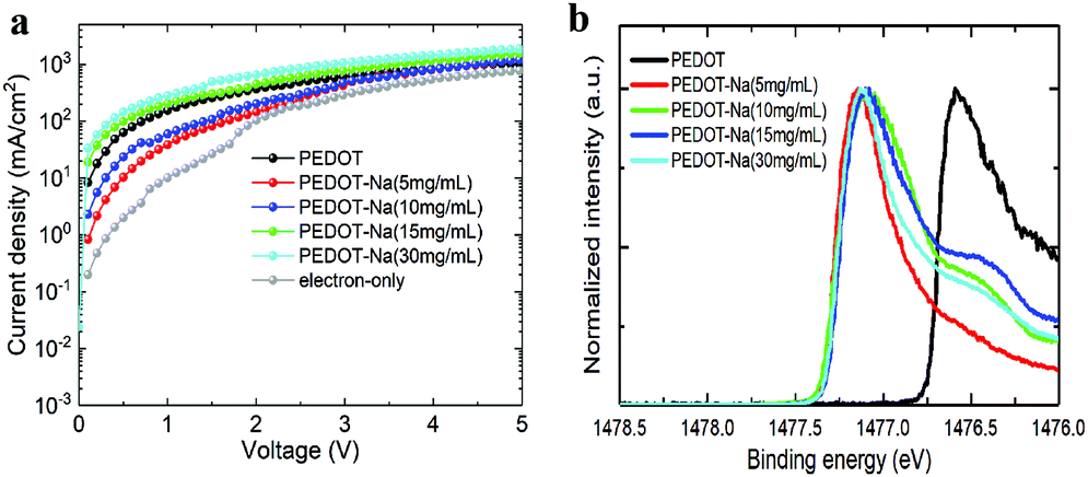 | ||
| Fig. 5 (a) J–V curves of the electron-only and hole-only devices, (b) XPS valence band spectra of PEDOT:PSS films with different NaCl doping concentrations. | ||
We draw a schematic diagram to better understand the charge transfer process and explain the mechanism of the doping induced improvement in our devices (Fig. 6). We know in light-emitting devices, the emitting layer was often designed to be thin in order to spatially confine electrons and holes for efficient radiative recombination. A thinner film can also help to lower reabsorption losses,5 however, its electronic structure can also be highly susceptible to the local electronic densities of states of the substrate and the interface in between. Especially for thinner films (below 35 nm) where the perovskite HOMO was found to be “pulled” toward that of PEDOT:PSS.40–42 Given that the perovskite film thickness is only 9nm in our case, it is expected that the holes can be easily injected into such a thin layer. This could explain why the hole current is higher than the electron current for the samples utilizing only PEDOT:PSS (Fig. 5(a)). These excess holes can be trapped or leaked to the EML/TPBi interface through such a thin perovskite layer (Fig. 6(a)). In the case of the optimized NaCl (10 mg mL−1) doping the work function of PEDOT:PSS was reduced, resulting in the decrease of the hole injection into the EML. This reduced hole current helped to maintain the recombination zone inside the perovskite EML or near the EML/HTL interface, effectively increasing radiative recombination. Additionally, the NaCl aggregates might help to reduce the direct contact of the perovskite with the quenching PEDOT:PSS (Fig. 6(b)). UV-vis and PL measurements (Fig. 4) both confirmed that they favored the growth of quasi-2D perovskite, which further increases the exciton binding energy in the perovskite EML. Thus the efficiency of NaCl doped PEDOT:PSS based PeLEDs was dramatically improved (Fig. 1(b–d)). The more effective radiative recombination together with the lower ohmic losses arising from the more conductive HTL via doping both contributed to lower turn-on voltage in Fig. 1(b). Finally, the more matched electron and hole injection resulted in the enhanced device lifetime shown in Fig. 1(e).
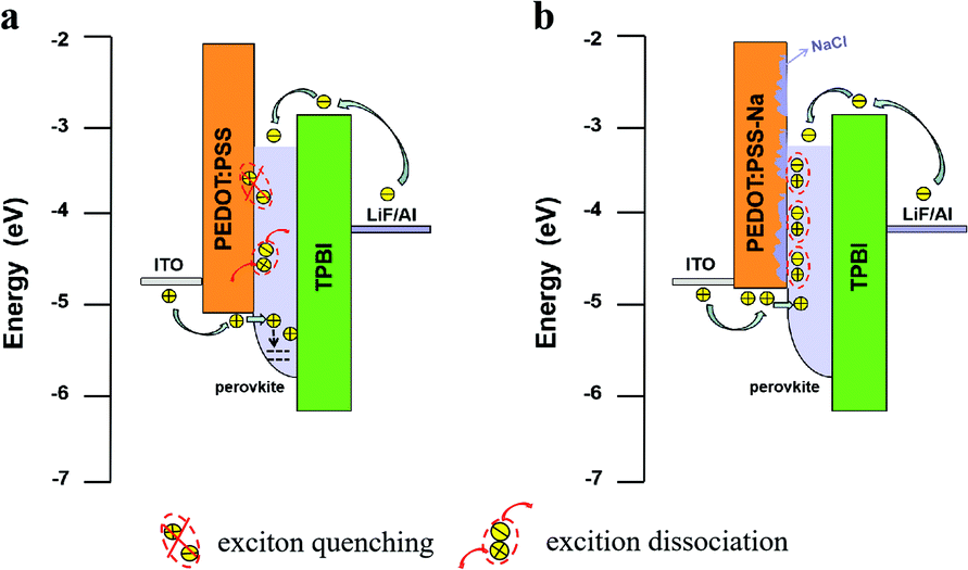 | ||
| Fig. 6 Schematic diagrams illustrate the charge transfer and recombination process in PeLEDs with PEDOT:PSS (a) and PEDOT-Na (10 mg mL−1) (b) as the HTL. | ||
Conclusions
In summary, we demonstrate the improvement of the efficiency of blue-green PeLEDs by the addition of NaCl in the PEDOT:PSS HTL. At the optimum NaCl doping concentration (10 mg mL−1) we observe three times higher luminance and above five times higher CE and LE compared to that of the PeLEDs utilizing pristine PEDOT:PSS HTL. The improvement is influenced by the precipitated NaCl aggregates at the PEDOT-Na surface which seed the growth of quasi-2D perovskite phases. Furthermore, they act as an ultrathin and discontinuous buffer layer that reduce the exciton quenching at the PEDOT:PSS/perovskite interface. The doping also caused the reduced work function of the PEDOT:PSS surface, leading to more balanced charge injection in the optimized device. When a higher concentration of NaCl was used (15 and 30 mg mL−1), the hole injection increased again which broke the charge balance, therefore the device performance started to decrease. These results highlight the importance of careful management of the hole-injecting interface in thin-film PeLEDs.Experimental section
Materials
All materials used were commercially purchased and used as received. Poly(3,4-ethylenedioxythiophene)polystyrene sulfonate (PEDOT:PSS, PVP AI 4083, FHC Solar) was purchased from Heraeus. Phenethylammonium bromide (PEABr, ≥98%), Formamidinium bromide (FABr, ≥98%), lead(II) bromide (PbBr2, 99.999%), dimethyl sulfoxide (DMSO, anhydrous, ≥99.9%), and ethyl acetate (≥99.5%) were purchased from Sigma Aldrich. Cesium bromide (CsBr, 99.9%), Lithium fluoride (LiF, 99.85%) were purchased from Alfa Aesar. 2,2′,2′′-(1,3,5-benzinetriyl)tris(1-phenyl-1H-benzimidazole) (TPBi, >99.5%) was purchased from Ossila.Preparation of perovskite light-emitting diodes
The NaCl doped HTL precursors were prepared by adding different amounts of NaCl into PEDOT:PSS aqueous solution and then vigorously stirring the solution before use. Firstly, the indium tin oxide (ITO) substrates were cleaned by sonication in acetone and isopropanol followed by drying in a N2 stream. Before the HTL deposition, the substrates were treated in oxygen plasma for 15 minutes to ensure good wetting properties. The PEDOT:PSS solutions with and without NaCl doping were then spin-coated on the ITO substrates with 4000 rpm for 30 s. Afterward, the substrates were heated on a hot plate in air at 150 °C for 30 minutes. The obtained PEDOT-Na films have thicknesses of around 25 nm measured by a profilometer (Fig. S6(b), ESI†).For the perovskite layer deposition, we followed the method developed by Jin et al.27 Briefly, 0.161 mmol PEABr, 0.09 mmol CsBr, 0.038 mmol FABr and 0.129 mmol PbBr2 were dissolved in 2 mL DMSO at first. Subsequently, the dissolved solution was spin-coated on the ITO/HTL substrates at 4000 rpm for 2 min. A drop of 300 μL ethyl acetate was applied at ∼21 s after the beginning of spin-coating to fascinate the crystallization and induced nanocrystal-pinning. Finally, TPBi (45 nm) and LiF/Al electrodes (1 nm/100 nm) were deposited using a thermal evaporation system under a high vacuum of ∼3 × 10⁻⁷ Torr through a shadow mask, yielding an active device area of 24 mm2.
Characterizations and measurements
Atomic force microscope (AFM) topographic images of PEDOT:PSS and NaCl doped PEDOT:PSS substrates as well as the perovskite films were taken by a DME DS 95 Dualscope AFM in tapping mode. The photoelectron spectroscopy measurements were performed using the VersaProbe I of PHI equipped with a monochromatized Al-Kα X-ray (hν = 1486 eV) source. The spectra are referenced to the Fermi edge of in situ sputter cleaned Ag foil. The base pressure of the measuring chamber during all experiments was kept in ∼10−9 mbar regime. Besides the XPS valence band spectra, we also used a macroscopic Kelvin probe (KP) from KP Technology to measure the work function of the PEDOT-Na samples. The system was equipped with a gold tip with a diameter of 2 mm and has an energetic resolution of ∼20 meV. We prepared three samples for each doping concentration to test, and three spots of each sample were tested during the measurement. Current–Voltage (I–V) characteristics of the HTLs were measured by Keithley 2636A source meter with a sweeping rate of 0.2 V s−1. Films thicknesses were determined on a Veeco Dektak 150 profilometer. The absorption of the perovskite films was measured with a UV-Vis (AvaSpec ULS3648) spectrometer. Photoluminescence spectra were obtained from a Jasco FP-6500 spectrofluorometer. The samples were excited by using a 370 nm monochromated Xenon lamp. The performance of PeLEDs was characterized by a calibrated Botest LIV functionality test system inside the glovebox. The scanning rate is 0.1 V s−1 with a delay time of 1 s.Conflicts of interest
The authors declare no competing financial interests.Acknowledgements
The authors acknowledge the financial support of the German Ministry for Education and Research (BMBF) under Grants No. FKZ: 03INT606AA, 03INT606AB and 03INT606AG. X. H. thanks the Chinese Scholarship Council (CSC) for support. The authors thank Prof. Dr Jan Philipp Hofmann from surface science of TU Darmstadt for access to their XPS. The author X. H further thanks Dr N. Jürgensen, Dr M. Held and Dr N. Strobel for helpful discussions.Notes and references
- J. Chen, S. Zhou, S. Jin, H. Li and T. Zhai, J. Mater. Chem. C, 2016, 4, 11–27 RSC.
- Y.-H. Kim, H. Cho, J. H. Heo, T.-S. Kim, N. Myoung, C.-L. Lee, S. H. Im and T.-W. Lee, Adv. Mater., 2015, 27, 1248–1254 CrossRef CAS PubMed.
- F. Zhang, J. Song, B. Han, T. Fang, J. Li and H. Zeng, Small Methods, 2018, 2, 1700382 CrossRef.
- H. Cho, S.-H. Jeong, M.-H. Park, Y.-H. Kim, C. Wolf, C.-L. Lee, J. H. Heo, A. Sadhanala, N. Myoung, S. Yoo, S. H. Im, R. H. Friend and T.-W. Lee, Science, 2015, 350, 1222–1225 CrossRef CAS PubMed.
- Z.-K. Tan, R. S. Moghaddam, M. L. Lai, P. Docampo, R. Higler, F. Deschler, M. Price, A. Sadhanala, L. M. Pazos, D. Credgington, F. Hanusch, T. Bein, H. J. Snaith and R. H. Friend, Nat. Nanotechnol., 2014, 9, 687–692 CrossRef CAS PubMed.
- T. Chiba, Y. Hayashi, H. Ebe, K. Hoshi, J. Sato, S. Sato, Y.-J. Pu, S. Ohisa and J. Kido, Nat. Photonics, 2018, 12, 681–687 CrossRef CAS.
- K. Lin, J. Xing, L. N. Quan, F. P. G. de Arquer, X. Gong, J. Lu, L. Xie, W. Zhao, D. Zhang, C. Yan, W. Li, X. Liu, Y. Lu, J. Kirman, E. H. Sargent, Q. Xiong and Z. Wei, Nature, 2018, 562, 245–248 CrossRef CAS PubMed.
- X.-B. Shi, Y. Liu, Z. Yuan, X.-K. Liu, Y. Miao, J. Wang, S. Lenk, S. Reineke and F. Gao, Adv. Opt. Mater., 2018, 6, 1800667 CrossRef.
- C. H. A. Li, Z. Zhou, P. Vashishtha and J. E. Halpert, Chem. Mater., 2019, 31, 6003–6032 CrossRef CAS.
- S. A. Rutledge and A. S. Helmy, J. Appl. Phys., 2013, 114, 133708 CrossRef.
- M. Luo, Y. Jiang, T. He and M. Yuan, APL Mater., 2020, 8, 040907 CrossRef CAS.
- M. K. Gangishetty, S. Hou, Q. Quan and D. N. Congreve, Adv. Mater., 2018, 30, 1706226 CrossRef PubMed.
- C. Mai, M. Li, H. Zheng, L. Mu, Y. Cun, D. Yu, J. Li, B. Zhang and J. Wang, Appl. Phys. Lett., 2020, 117, 012107 CrossRef.
- X.-F. Peng, X.-Y. Wu, X.-X. Ji, J. Ren, Q. Wang, G.-Q. Li and X.-H. Yang, J. Phys. Chem. Lett., 2017, 8, 4691–4697 CrossRef CAS PubMed.
- Y. Shi, W. Wu, H. Dong, G. Li, K. Xi, G. Divitini, C. Ran, F. Yuan, M. Zhang, B. Jiao, X. Hou and Z. Wu, Adv. Mater., 2018, 30, 1800251 CrossRef PubMed.
- Z. Li, K. Cao, J. Li, X. Du, Y. Tang and B. Yu, Org. Electron., 2020, 81, 105675 CrossRef CAS.
- C. Lin, P. Chen, Z. Xiong, D. Liu, G. Wang, Y. Meng and Q. Song, Nanotechnology, 2018, 29, 075203 CrossRef PubMed.
- D. B. Kim, J. C. Yu, Y. S. Nam, D. W. Kim, E. D. Jung, S. Y. Lee, S. Lee, J. H. Park, A.-Y. Lee, B. R. Lee, D. Di Nuzzo, R. H. Friend and M. H. Song, J. Mater. Chem. C, 2016, 4, 8161–8165 RSC.
- Z. Wang, Z. Li, D. Zhou and J. Yu, Appl. Phys. Lett., 2017, 111, 233304 CrossRef.
- R. L. Z. Hoye, M.-L. Lai, M. Anaya, Y. Tong, K. Gałkowski, T. Doherty, W. Li, T. N. Huq, S. Mackowski, L. Polavarapu, J. Feldmann, J. L. MacManus-Driscoll, R. H. Friend, A. S. Urban and S. D. Stranks, ACS Energy Lett., 2019, 4, 1181–1188 CrossRef CAS PubMed.
- Z. Li, Z. Chen, Y. Yang, Q. Xue, H.-L. Yip and Y. Cao, Nat. Commun., 2019, 10, 1027 CrossRef PubMed.
- Z. Tan, J. Luo, L. Yang, X. Li, Z. Deng, L. Gao, H. Chen, J. Li, P. Du, G. Niu and J. Tang, Adv. Opt. Mater., 2020, 8, 1901094 CrossRef CAS.
- J. Dagar, K. Hirselandt, A. Merdasa, A. Czudek, R. Munir, F. Zu, N. Koch, T. Dittrich and E. L. Unger, Sol. RRL, 2019, 3, 1900088 CrossRef.
- H. Lee, A. Kim, H.-C. Kwon, W. Yang, Y. Oh, D. Lee and J. Moon, ACS Appl. Mater. Interfaces, 2016, 8, 29419–29426 CrossRef CAS PubMed.
- L. Hu, K. Sun, M. Wang, W. Chen, B. Yang, J. Fu, Z. Xiong, X. Li, X. Tang, Z. Zang, S. Zhang, L. Sun and M. Li, ACS Appl. Mater. Interfaces, 2017, 9, 43902–43909 CrossRef CAS PubMed.
- D. Di Girolamo, N. Phung, M. Jošt, A. Al-Ashouri, G. Chistiakova, J. Li, J. A. Márquez, T. Unold, L. Korte, S. Albrecht, A. Di Carlo, D. Dini and A. Abate, Adv. Mater. Interfaces, 2019, 6, 1900789 CrossRef.
- Y. Liu, J. Cui, K. Du, H. Tian, Z. He, Q. Zhou, Z. Yang, Y. Deng, D. Chen, X. Zuo, Y. Ren, L. Wang, H. Zhu, B. Zhao, D. Di, J. Wang, R. H. Friend and Y. Jin, Nat. Photonics, 2019, 13, 760–764 CrossRef CAS.
- F. Hermerschmidt, F. Mathies, V. R. F. Schröder, C. Rehermann, N. Z. Morales, E. L. Unger and E. J. W. List-Kratochvil, Mater. Horiz., 2020, 7, 1773–1781 RSC.
- Y. Xia, K. Sun and J. Ouyang, Energy Environ. Sci., 2012, 5, 5325–5332 RSC.
- F. Wu, P. Li, K. Sun, Y. Zhou, W. Chen, J. Fu, M. Li, S. Lu, D. Wei, X. Tang, Z. Zang, L. Sun, X. Liu and J. Ouyang, Adv. Electron. Mater., 2017, 3, 1700047 CrossRef.
- T. Liu, Y. Jiang, M. Qin, J. Liu, L. Sun, F. Qin, L. Hu, S. Xiong, X. Jiang, F. Jiang, P. Peng, S. Jin, X. Lu and Y. Zhou, Nat. Commun., 2019, 10, 878 CrossRef.
- H. Tsai, W. Nie, J.-C. Blancon, C. C. Stoumpos, R. Asadpour, B. Harutyunyan, A. J. Neukirch, R. Verduzco, J. J. Crochet, S. Tretiak, L. Pedesseau, J. Even, M. A. Alam, G. Gupta, J. Lou, P. M. Ajayan, M. J. Bedzyk, M. G. Kanatzidis and A. D. Mohite, Nature, 2016, 536, 312–316 CrossRef CAS PubMed.
- N. Liu, P. Liu, H. Ren, H. Xie, N. Zhou, Y. Gao, Y. Li, H. Zhou, Y. Bai and Q. Chen, ACS Appl. Mater. Interfaces, 2020, 12, 3127–3133 CrossRef CAS PubMed.
- Z. Wang, F. Wang, W. Sun, R. Ni, S. Hu, J. Liu, B. Zhang, A. Alsaed, T. Hayat and Z. A. Tan, Adv. Funct. Mater., 2018, 28, 1804187 CrossRef.
- J. Hwang, F. Amy and A. Kahn, Org. Electron., 2006, 7, 387–396 CrossRef CAS.
- S. E. Shaheen, G. E. Jabbour, M. M. Morrell, Y. Kawabe, B. Kippelen, N. Peyghambarian, M.-F. Nabor, R. Schlaf, E. A. Mash and N. R. Armstrong, J. Appl. Phys., 1998, 84, 2324–2327 CrossRef CAS.
- J. Kim, M. Kim, J. W. Kim, Y. Yi and H. Kang, J. Appl. Phys., 2010, 108, 103703 CrossRef.
- S. W. Shi, D. G. Ma and J. B. Peng, Eur. Phys. J. Appl. Phys., 2007, 40, 141–144 CrossRef CAS.
- J. M. Zhao, Y. Q. Zhan, S. T. Zhang, X. J. Wang, Y. C. Zhou, Y. Wu, Z. J. Wang, X. M. Ding and X. Y. Hou, Appl. Phys. Lett., 2004, 84, 5377–5379 CrossRef CAS.
- E. M. Miller, Y. Zhao, C. C. Mercado, S. K. Saha, J. M. Luther, K. Zhu, V. Stevanović, C. L. Perkins and J. van de Lagemaat, Phys. Chem. Chem. Phys., 2014, 16, 22122–22130 RSC.
- S. Olthof and K. Meerholz, Sci. Rep., 2017, 7, 40267 CrossRef CAS PubMed.
- S. Lee, D. B. Kim, I. Hamilton, M. Daboczi, Y. S. Nam, B. R. Lee, B. Zhao, C. H. Jang, R. H. Friend, J.-S. Kim and M. H. Song, Adv. Sci., 2018, 5, 1801350 CrossRef PubMed.
Footnote |
| † Electronic supplementary information (ESI) available. See DOI: 10.1039/d0tc06058e |
| This journal is © The Royal Society of Chemistry 2021 |