
 Open Access Article
 This Open Access Article is licensed under a Creative Commons Attribution-Non Commercial 3.0 Unported Licence
Elimination of interlayer Schottky barrier in borophene/C4N4 vdW heterojunctions via Li-ion adsorption for tunneling photodiodes†
Cancan
Zheng
a,
Cong
Zhou
a,
Man
Shi
a,
Haiyan
Li
a,
Nianxi
Dou
a,
Zhihao
Ma
a,
Feifei
Xia
b,
Yuanyuan
He
 *a and
Jianwei
Zhao
*a
*a and
Jianwei
Zhao
*a
aCollege of Material and Textile Engineering, Key Laboratory of Yarn Materials Forming and Composite Processing Technology, Jiaxing University, Jiaxing, 314001, Zhejiang, People's Republic of China. E-mail: heyy@zjxu.edu.cn; jwzhao@zjxu.edu.cn
bSchool of Chemical and Environmental Engineering, Jiangsu University of Technology, Changzhou, 213001, Jiangsu, People's Republic of China
First published on 8th March 2021
Abstract
The nonzero interlayer Schottky barrier leads to a compromise between photodetectivity and photoresponsivity in photodiodes based on vdW heterojunctions. Seeking for the appropriate vdW heterojunction with Ohmic contact and a high tunneling barrier is of great significance to realize high-performance photodiodes. We built borophene/C4N4 (B/C4N4) vdW heterojunctions with a reduced interlayer Schottky barrier, by combining density functional theory and non-equilibrium Green's function. The adsorption of Li-ions can further tune its Schottky contact into n-type Ohmic contact. The electronic properties of the Li-ion-adsorbed B/C4N4 vdW heterojunction, including the separation of hole–electron pairs, the work function, as well as the effective mass of carrier, can be modulated by changing the adsorption site of Li-ions. B/C4N4/Li shows the most excellent absorbing capability of the infrared illumination and the strongest negative rectification, due to the highest interlayer tunneling barrier. The bottom surface of the C4N4 sublayer is the optimal adsorption site of Li-ions, for the potential application of B/C4N4 vdW heterojunctions in tunneling photodiodes. Our work unveils the great significance of Li-ion adsorption in modulating the interlayer Schottky and tunneling barriers in vdW heterojunctions, thus improving their device performance.
1. Introduction
Semiconductor-based photodiodes, as a photoelectric sensing component to convert optical signals into photocurrent, has been widely studied and applied in many areas, such as image sensing, environmental monitoring, surveillance and spectroscopy.1–4 Schottky barrier photodiodes are considered superior to p-i-n photodiodes, metal-semiconductor–metal photodiodes, and so on, in terms of their low power consumption, large current, and ultrahigh response speed.5–8 Recently, van der Waals (vdW) heterostructures, which are formed by stacking different two-dimensional (2D) semiconductors vertically through vdW forces, have attracted the interest of a growing number of researchers. vdW heterojunctions have a large specific surface area, and their bandgap can be adjusted, while suppressing the recombination rate of the photogenerated carriers, which is greatly beneficial to the photoelectric process.9 Unfortunately, the interlayer Fermi level pinning effect in vdW heterojunctions often leads to Schottky barriers at the interface and thus probably results in undesirable large contact resistance.10 As a result, an inevitable compromise between photodetectivity and photoresponsivity often emerges in Schottky barrier photodiodes based on vdW heterojunctions.11 In 2017, Zhai's group demonstrated the main positive contribution of high tunneling barrier to the high photocurrent, on the basis of which a highly sensitive WSe2/SnS2 photodiode was fabricated, exhibiting both ultrahigh photodetectivity of 1.29 × 10¹³ Jones (Iph/Idark ratio of ≈106) and photoresponsivity of 244 A W−1 at a reverse bias under the illumination of 550 nm light (3.77 mW cm−2).12 Hence, seeking for the appropriate vdW heterojunction with Ohmic contact and a high tunneling barrier is of great significance to construct high-performance photodiodes.Monolayer C4N4, as a novel p-type semiconductor, is competitive in the construction of vdW heterojunctions for applications in nanoscale electronics and optoelectronics, since it is reported that the Ohmic contact between C4N4 and graphyne could improve the conductivity of Li–S battery electrodes.13 Moreover, monolayer C4N4 is predicted to display a strong infrared response, opening the possibilities of C4N4-based vdW heterojunctions for tunneling photodiodes.14 Yang et al. reported the fabrication of C3N by polymerization of 2,3-diaminophenazine (DAP), in which both N and C atoms are distributed homogeneously.15 They provided a feasible way to control the distribution of N atoms for improving the experimental methods of C4N4 synthesis. By comparing the cohesive energy per atom and the n-layer exfoliation energy per unit area, the C4N4 monolayer is more stable than many other carbonitride monolayers and can be easily prepared from its bulk forms using a similar experimental mechanical exfoliation method to that of graphene.16–18 It is possible to prepare C4N4 monolayers by experiments successfully, even though they have not been achieved hitherto. To eliminate the Schottky barrier, theoretical assessments suggest that monolayer borophene can be used as a substitute for the traditional noble metal for contact with monolayer C4N4.19 For building tunneling photodiodes based on vdW heterojunctions, doping control is critical to further reduce the interlayer Schottky barrier. Considerable time and effort have been expended to develop effective doping strategies, such as thickness engineering,20,21 surface modifications,22–24 atomic substitutions,25–27 and mechanical strain,28,29 however these are not applicable to vdW heterojunctions, due to their peculiar structures. Experimentally, ionic intercalations have been developed to complementarily dope vdW materials for diode devices, providing a potential method to realize tunneling photodiodes based on borophene/C4N4 (B/C4N4) vdW heterojunctions.30
In this study, based on density functional theory (DFT), we built B/C4N4 vdW heterojunctions by stacking monolayer borophene and C4N4 vertically and further decorating them with Li-ions. The electronic properties of free-standing borophene and C4N4 monolayers, including the separation of hole–electron pairs (Δρ), work function (ΔΦ), and effective mass of carriers (Δm*), are rationally modulated by the combination of vertical stacking and Li-ion adsorption. Most significantly, the interlayer Schottky contact in B/C4N4 vdW heterojunctions has been transformed into an Ohmic contact via the adsorption of Li-ions. By modulating Li-ions from the top to bottom site on B/C4N4 vdW heterojunctions, the increasing tunneling barrier will not only enhance the optical absorption in the entire infrared region, but also improve the negative rectification behavior. This work shows the great significance of Li-ion adsorption on modulating the interlayer energy barrier in vdW heterojunctions, paving the way towards applications in high-performance tunneling photodiodes.
2. Computational details
A vertical interface consisting of borophene and C4N4 monolayers, i.e. a B/C4N4 van der Waals (vdW) heterojunction, was built by matching the two crystals. For comparison, bilayer borophene and bilayer C4N4 were modeled as vdW homojunctions.31–33 In the Atomistix-toolkit Virtual-nano-lab (ATK-VNL) package, the linear combination of atomic orbitals (LCAO) techniques was utilized to optimize the geometry of the stacking superlattice and to calculate its electronic properties.34,35 A vacuum layer of about 25 Å was introduced to minimize the spurious interaction between neighboring layers. A specialized Grimme's approach (DFT-D3) was adopted to correct interfacial dispersion, taking van der Waals interactions into account.36 The scalar-relativistic (SG15) optimized norm-conserving Vanderbilt (ONCV) pseudopotentials were employed with an energy cutoff of 100 Hartree, combined with the plane-wave basis set.37 The k-point mesh of 10 × 1 × 10 was selected in the Brillouin zone during geometric optimization. The position of the upper layer relative to the bottom layer was optimized until the energy and stress error were less than 1.0 × 10⁻³ eV Å−1 and 5.0 × 10⁻³ GPa, respectively. A much denser k-point mesh (15 × 1 × 15) was applied in the band structure and density of states (DOS) calculation. The electron–electron interactions were treated using the DFT-1/2 method considering the electron spin within Perdew–Burke–Ernzerhoff (PBE) parameterization, which has been widely applied to calculate the bandgap with more accuracy in a feasible time.38,39Furthermore, the ballistic transport behavior of the two-probe B/C4N4 vdW heterojunction was systematically analyzed, by using DFT combined with the non-equilibrium Green's function (NEGF) method. Monolayer borophene with a length of 20.74 Å was used as the left electrode, whereas monolayer C4N4 with the same length was used as the right electrode. In the central region, monolayer borophene and C4N4 were stacked with each other with a length of 20.74 Å, which was further relaxed until the force on each atom was less than 0.5 eV. The wave functions and other physical operators are expanded with a double zeta polarized (DZP) LCAO basis and the fineness of the real space grid is determined by an equivalent plane wave cut-off of 100 Hartree. The current and transmission spectra were calculated by using the NEGF-implemented ATK-VNL package. The current was obtained by integrating the transmission within the bias window:40,41
 | (1) |
3. Results and discussion
Among all possible allotropes in borophene, the free-standing β12 phase derived from the α-sheet structure is thermodynamically, mechanically, and dynamically the most stable.42–44 In the following discussion, β12 borophene is chosen as the material to build a van der Waals heterojunction with C4N4 monolayers. As shown in Fig. 1a–e, monolayer borophene has a planar structure with anisotropic corrugation. The optimized constant lattices in monolayer C4N4 are a = 6.08 Å and c = 3.58 Å, with a buckling height of ≈ 0.35 Å. During the formation of the B/C4N4 vdW heterojunction, we adapt the borophene supercell to vertically stack with 1 × 3 C4N4, in which the corresponding mismatch of the lattice constants is less than 2%. There is an angle of 29.0° between the arrangement of vacancies and the z-direction in the monolayer borophene supercell. In the formed B/C4N4 vdW heterojunction, the relative position of borophene is freely relaxed, while the C4N4 sublayer remains frozen. After geometric optimization, the vertical distance between borophene and C4N4 is dy = 3.26 Å. Compared with bilayer borophene (B/B) and bilayer C4N4 (C4N4/C4N4) as van der Waals (vdW) homojunctions (dy = 3.15 and 2.93 Å, respectively), the above B/C4N4 vdW heterojunction possesses the widest interlayer distance. The binding energy (Eb) of the bilayer system is defined as:
| Eb = (Eupper+bottom − Eupper − Ebottom)/(NB + NC + NN), | (2) |
 | ||
| Fig. 1 Top and side views of free-standing (a) borophene and (b) C4N4 monolayers. Optimized configurations of (c) bilayer borophene (B/B), (d) bilayer C4N4 (C4N4/C4N4) as vdW homojunctions, and (e) B/C4N4 vdW heterojunctions. The lowest energy structures for Li-ion-decorated B/C4N4 vdW heterojunctions with (f) top, (g) sandwiched, and (h) bottom adsorption sites, respectively. | ||
| Superlattice | a (Å) | c (Å) | E b (eV per atom) | d y (Å) | L Li–X (Å) |
|---|---|---|---|---|---|
| a Before Li-ions adsorption: Eb = (Eupper+bottom − Eupper − Ebottom)/(NB + NC + NN), where Eupper+bottom, Eupper, and Ebottom are the relaxed energies of the bilayer systems, the isolated upper and bottom layers, respectively, and NB, NC, and NN are the numbers of B atoms in the borophene supercell, and C and N atoms in the C4N4 supercell. b After Li-ion adsorption: Eb = (ELi+B+C4N4 − NLiELi − EB − EC4N4)/(NB + NC + NN + NLi), where ELi+B+C4N4 denotes the total energy of Li-adsorbed B/C4N4 vdW heterojunctions, whereas ELi, EB, and EC4N4 represent the total energies of isolated Li-ion, monolayer borophene and C4N4 supercells, respectively. NLi, NB, NC, and NN are the numbers of Li-ions, and B, C, and N atoms in a unit supercell of the adsorption system. | |||||
| B/B | 5.86 | 10.13 | −0.045a | 3.15 | — |
| C4N4/C4N4 | 6.08 | 10.77 | −0.036a | 2.93 | — |
| B/C4N4 | 6.08 | 10.77 | −0.010a | 3.26 | — |
| Li/B/C4N4 | 6.08 | 10.77 | −0.22b | 3.26 | 2.25 (Li–B) |
| B/Li/C4N4 | 6.08 | 10.77 | −0.24b | 3.50 | 2.30 (Li–B) |
| 2.21 (Li–N) | |||||
| B/C4N4/Li | 6.08 | 10.77 | −0.13b | 3.18 | 1.99 (Li–N) |
We further decorate Li-ions on the top, sandwiched, and bottom sites of the B/C4N4 vdW heterojunction, respectively. Li-ions are inclined to be adsorbed on the hollow site of the vacancies. By comparing Fig. 1f–h and Fig. S1 (ESI†), when Li-ions are adsorbed on the top and bottom sites of the B/C4N4 vdW heterojunctions (which are called Li/B/C4N4 and B/C4N4/Li for short, respectively), the lengths of the Li–B bond and Li–N bond are 2.25 and 1.99 Å, respectively, irrespective of the formation of B/C4N4 vdW heterojunctions. Meanwhile, the interlayer distance in B/C4N4 vdW heterojunctions is also insensitive to the adsorption of Li-ions. However, the insertion of Li-ions between borophene and C4N4 has expanded the interlayer distance by 7.36% from 3.26 Å to 3.50 Å. It is commonly believed that such an expanded bilayer, considered as an ideal structure for Li-ion batteries, can provide pathways for rapid electron transfer and further enhance the gravimetric and areal capacities.46,47
The stability of Li-ion adsorption on B/C4N4 vdW heterojunctions is evaluated by the binding energy (Eb) of each Li-ion according to the following formula:48,49
| Eb = (ELi+B+C4N4 − NLiELi − EB − EC4N4)/(NLi + NB + NC + NN), | (3) |
 | ||
| Fig. 2 Top views of ELF isosurfaces for (a) borophene and (b) C4N4 monolayers. Side views of ELF maps for (c) B/B, (d) C4N4/C4N4 vdW homojunctions, and (e–h) B/C4N4 vdW heterojunctions before and after Li-ion adsorption at the top, sandwiched, and bottom sites, respectively. | ||
The above bilayer systems before and after Li-ion adsorption can be classified into two types of adsorption systems, according to the type of substrate. Specifically, the borophene-substrate-systems consist of Li/B monolayer, B/B vdW homojunction, and B/C4N4, B/Li/C4N4, and B/C4N4/Li vdW heterojunctions, in which Li-ions, borophene, C4N4, Li top-site-adsorbed C4N4 (Li/C4N4), and Li bottom-site-adsorbed C4N4 (C4N4/Li) monolayers are considered as the surface adsorbates. The cases of C4N4-substrate-systems are similar to the borophene-substrate-adsorption systems. Through this classification strategy, we explored the doping effect of various adsorbates on the electronic properties of borophene and C4N4 monolayers.
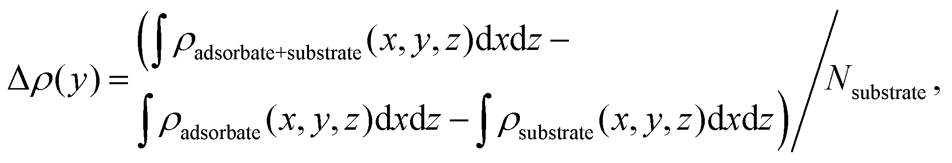
Mulliken charge densities in the above adsorption systems were calculated in Fig. 3a, to investigate the effect of vertical stacking and Li-ion adsorption on the interfacial separation of hole–electron pairs of bilayer structures. The electron density difference (Δρ) is defined as follows:51,52
 | (4) |
 | ||
| Fig. 3 (a) Mulliken charge transfer (Δρ) between surface adsorbates and borophene (C4N4) substrates, (b) change of work function (ΔΦ), and (c and d) changes of electron effective mass (Δme) and hole effective mass (Δmh) on borophene (C4N4) substrates at the GGA-1/2 level. | ||
The variation of work function before and after surface adsorption will provide guidelines on how to tune the carrier concentration on borophene and C4N4 monolayers by the choice of surface adsorbate. The electrostatic potential calculations are performed to probe changes of the work function (ΔΦ = Φadsorbate+substrate − Φsubstrate) for borophene and C4N4 monolayers with different surface modifications.54 The local density approximation (LDA) method predicted that the Φ values of isolated borophene, C4N4, and Li-ions are ca. 5.59, 7.12, and 2.29 eV, respectively. As shown in Fig. 3b, the formation of B/C4N4 vdW heterojunctions can decrease the work function of bottom C4N4 by 0.46 eV, meanwhile increasing that of upper borophene by 1.74 eV. As a result, n-type doping of C4N4 and p-type doping of borophene are effectively achieved. Conversely, the formation of B/B and C4N4/C4N4 vdW homojunctions has a negligible effect on the work function, owing to the minimum separation of hole–electron pairs. The adsorption of Li-ions may further change the work function in B/C4N4 vdW heterojunctions. For upper borophene, the adsorption of Li/C4N4 will increase its work function by 1.24 eV, whereas C4N4/Li can decrease its work function by 3.27 eV, showing an opposite doping effect. This is because the direct B–Li ionic bonds in B/Li/C4N4 are so strong that numerous electrons are donated from Li-ions to borophene, whereas electrons are accumulated on the C4N4 sublayer in B/C4N4/Li, because of the strong electron-donating capabilities of borophene and Li-ions. As for the C4N4 substrate, the adsorption of Li/B effectively decreases the work function by 3.96 eV, showing a stronger n-type doping effect than B/Li (−2.27 eV), due to the fact that borophene in B/Li/C4N4 shares a proportion of electrons injected from the inserted Li-ions.
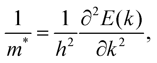
The effective mass of carriers (m*) is another critical factor to describe the influence of surface modification on the interfacial carrier transport in adsorption systems. m* in the adsorption system is assessed by fitting parabolic functions to the conduction band bottom (valence band top) as follows:55
 | (5) |
Fig. 4a and b show the band structures of pristine borophene and C4N4 monolayer before and after Li-ion adsorption. The bands projected to borophene, C4N4 and Li-ions are indicated by red, blue, and yellow colors, respectively. Obviously, the electron-donating capability of Li-ions is so strong that their adsorption can effectively enhance the metallic property of borophene and even tune the C4N4 monolayer from p-type into metallic. The domination of interlayer vdW interaction in bilayer systems is quite different from the above ionic interaction in modulating the band structure. Fig. 4c demonstrates that the original band structures of pristine borophene and C4N4 monolayers are well preserved in B/B and C4N4/C4N4 vdW homojunctions, owing to the negligible separation of hole–electron pairs. In contrast, the strong separation of hole–electron pairs has enhanced the interlayer coupling effect and thus opened the bandgap of borophene to 0.18 eV. As a result, the band hybridization in the B/C4N4 vdW heterojunction is much stronger than those in the corresponding vdW homojunctions.
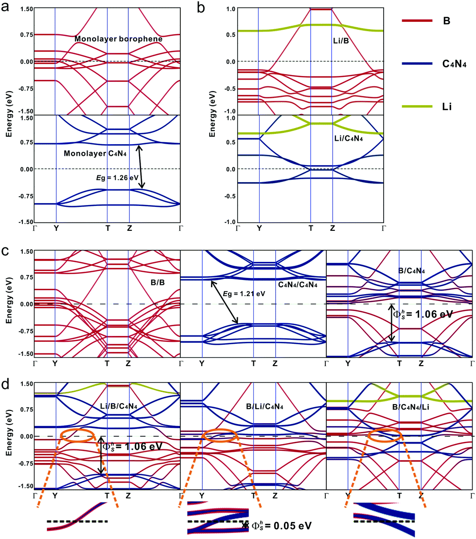 | ||
| Fig. 4 Band structures for pristine borophene and C4N4 monolayers (a) before and (b) after Li-ion adsorption, (c) bilayer systems consisting of borophene and C4N4, and (d) B/C4N4 vdW heterojunctions with Li-ions at the top, sandwiched, and bottom sites, respectively. Red line: borophene; blue line: C4N4; yellow line: adsorbed Li-ions. The Fermi level is set at zero energy and denoted by the dashed line. | ||
A large Schottky barrier height (SBH) impedes the interlayer electronic transport and degrades the performance of a photodiode based on the p–n junction. The homogeneous stacking of materials in the bottom and upper sublayers makes B/B and C4N4/C4N4 vdW homojunctions inappropriate to build p–n junctions, from the point of view of photodiode application. When using borophene and C4N4 monolayers as the left and right electrodes, it will be very important to explore the interfacial Schottky barrier height (ΦS) in B/C4N4 vdW heterojunctions before and after Li-ions adsorption. ΦS is defined by the difference between the CBM/VBM of the C4N4 sublayer and the Fermi level (EF) of the borophene sublayer and can be attained from the band structures of B/C4N4 vdW heterojunctions.45 The vertical electron SBH (ΦeS) in B/C4N4 vdW heterojunctions is 0.013 eV, whereas the vertical hole SBH (ΦhS) is 1.06 eV, forming an n-type Schottky contact. As shown in the enlarged band structure near EF in Fig. 4d, the adsorption of Li-ions at the top site has decreased the vertical ΦeS to zero, since the CBM of C4N4 has shifted downward to lower than EF, while keeping ΦhS unchanged. By changing the adsorption of Li-ions from the top to the sandwiched site, the vertical ΦhS has been dramatically reduced to 0.05 eV. Furthermore, in the B/C4N4/Li vdW heterojunction, both the CBM and VBM projected on C4N4 are shifted across EF, thus resulting in zero Schottky barrier. Therefore, the Schottky contact between C4N4 and borophene can be effectively tuned into Ohmic contact, via optimizing the adsorption site of Li-ions. By comparing the band structures of B/C4N4 vdW heterojunctions with Li-ions on different adsorption sites, it is observed that CBM across EF in B/C4N4/Li is mainly contributed by C4N4, whereas that in Li/B/C4N4 is dominated by borophene. This is largely due to the stronger charge transfer between Li-ions and the sublayer in direct contact. The projected density of states (PDOS) in Fig. 5 indicates that the bottom C4N4 sublayer becomes more metallized, by moving down the adsorption site of Li-ions in the B/C4N4 vdW heterojunctions. Accordingly, the Fermi level is dominated by C4N4, which further validates the leading role of C4N4 in the n-type Ohmic contact between borophene and C4N4 in B/C4N4/Li. Such n-type Ohmic contact is highly desirable to the application of vdW heterojunctions in high-performance electronic and optoelectronic devices, because it can promote the electronic transport efficiency.56,57
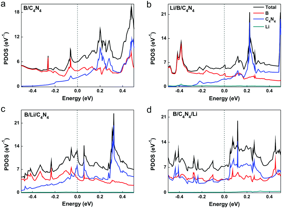 | ||
| Fig. 5 Projected density of states (PDOS) of B/C4N4 vdW heterojunctions (a) before and (b–d) after Li-ion adsorption at the top, sandwiched, and bottom sites, respectively. The Fermi level is set at zero energy and denoted by the dashed line. | ||
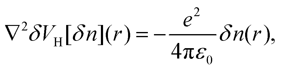
There also exists another type of vertical energy barrier in the above B/C4N4 vdW heterojunctions, namely, the tunneling barrier. Different from the Schottky barrier, electrons and holes can be effectively separated with less energy loss in the tunneling barrier, thus generating photoelectric conversion.58–60 Generally, the tunneling barrier height is dependent on the asymmetry of the heterojunction and can be evaluated by the Hartree difference potential (δVH).61,62 Herein, δVH is calculated from the electron difference density as:
 | (6) |
 | (7) |
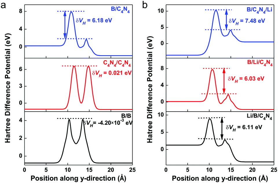 | ||
| Fig. 6 The interlayer Hartree difference potentials for (a) bilayer systems consisting of borophene and C4N4 monolayers, and (b) B/C4N4 vdW heterojunctions with Li-ions at the top, sandwiched, and bottom adsorption sites, respectively. | ||
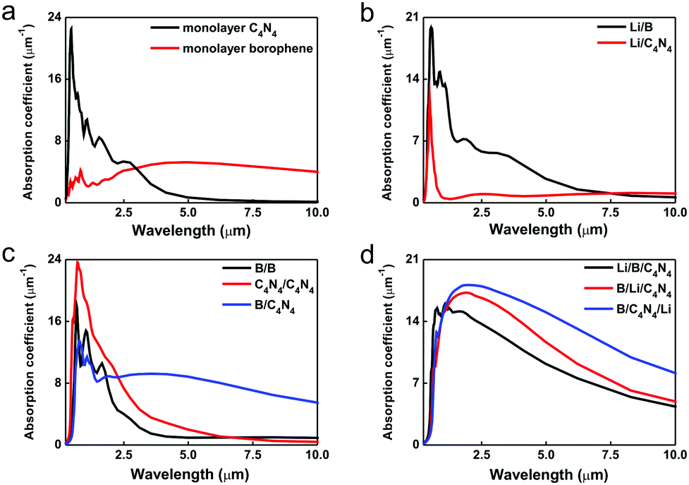
We further calculated the optical absorption coefficients in various bilayer systems in comparison with isolated borophene and C4N4 monolayers. Normally, a wide direct bandgap can induce larger probabilities of electron migration under illumination. As shown in Fig. 7a and b, the adsorption of Li-ions on monolayer C4N4 severely suppresses its high absorption peak (>23.55 μm−1) in a wide solar spectrum from the ultraviolet region (0.29 μm) to the mid-infrared (2.76 μm), due to the disappearance of the bandgap in Li/C4N4. In contrast, the optical absorption peak of pristine borophene in the range from 0.25 to 0.83 μm has been remarkably intensified nearly 5 times by the adsorption of Li-ions and extended from the near-infrared to mid-infrared region as far as >7.48 μm, since the adsorbed Li-ions on the borophene substrate provide states shallower than that in the Li/C4N4 system. As for the formation of a bilayer structure, the wide bandgap in C4N4/C4N4 vdW homojunctions results in its sharp optical absorption peak in the visual region, whereas the higher tunneling barrier in B/C4N4 vdW heterojunctions leads to its wider optical absorption peak in the entire infrared region (>1.46 μm). The integral area ratio of infrared light reaches nearly 50% in the solar radiation spectrum, much larger than those of ultraviolet and visual lights. The strong optical response under infrared illumination allows the B/C4N4 vdW heterojunctions to make the best use of sunlight. In view of the poor infrared-light capturing capabilities, B/B and C4N4/C4N4 vdW homojunctions will not be considered in the following electronic transport behavior study for photodiode applications. In B/C4N4 vdW heterojunctions with Li-ion adsorption, the optical absorption peak has been enhanced by approximately 14% without a remarkable shift, by changing the adsorption site from the top to the bottom, since the tunneling barrier becomes higher. Therefore, the adsorption of Li-ions on the bottom site provides a feasible method to enhance its optical absorption, which would be conducive to improving the performance of optoelectronic nanodevices based on B/C4N4 vdW heterojunctions.
 | ||
| Fig. 7 Optical absorption spectra for borophene and C4N4 monolayers (a) before and (b) after Li-ion adsorption, (c) bilayer systems consisting of borophene and C4N4, and (d) B/C4N4 vdW heterojunctions with Li-ions on various adsorption sites, respectively. | ||
The effect of tunneling barrier on the device performance of a photodiode based on B/C4N4 vdW heterojunctions can also be reflected by the change of its quantum transport behavior via Li-ion adsorption. Fig. 8a displays the schematic diagram of a two-probe B/C4N4 vdW heterojunction system with Li-ion adsorption, in which the Li-ion adsorption can be manipulated between the top, sandwiched, and bottom sites. In the central region, the supercell of B/C4N4 vdW heterojunctions repeats twice along the z-direction, i.e. the direction of the electric field.
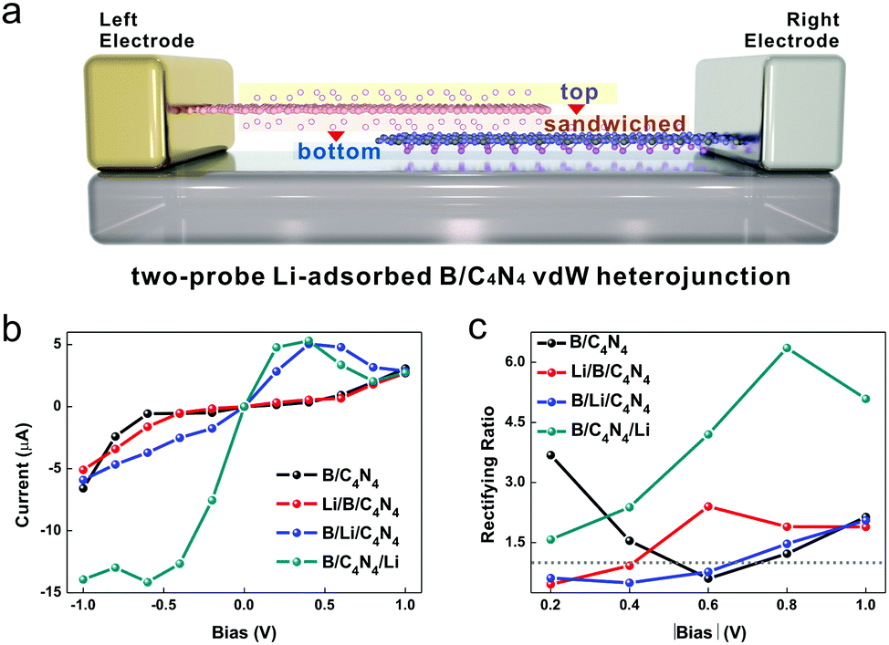 | ||
| Fig. 8 (a) Schematic diagram of two-probe B/C4N4 vdW heterojunction with Li-ion adsorption, in which the adsorption varies between the top and bottom sites. (b) The dependence of current and (c) the rectifying ratio on bias voltage in B/C4N4 vdW heterojunctions before and after Li-ion adsorption, respectively. | ||
We plot the current–bias (I–Vb) dependence curves of B/C4N4 vdW heterojunctions with different Li-ions adsorption sites in Fig. 8b. In B/C4N4 vdW heterojunction without the adsorption of Li-ions, the reverse current (−1.0 to 0 V) decreases rapidly, which is much more remarkable than the forward one (1.0 to 0 V), by descending |Vb|. As a result, B/C4N4 shows an obvious negative rectification behavior. To quantitatively illustrate the rectifying behavior, we define the rectifying ratio (R) as R = |I(−Vb)/I(+Vb)|. R = 1 indicates no rectification effect, and R > 1 denotes a higher reverse current, i.e. a negative rectification, whereas R < 1 represents a higher forward current, known as a positive rectification.63,64 The Vb–R curves in B/C4N4 vdW heterojunctions with various Li-ion adsorption sites are shown in Fig. 8c. The R value of B/C4N4 vdW heterojunctions reaches the maximum of 3.68 at |Vb| = 0.2 V and the minimum of 0.60 at |Vb| = 0.6 V. The reversed rectifying status in B/C4N4 reveals that the metallic-semiconductive asymmetry is tunable by changing the direction of the electric field. The R value in Li/B/C4N4 vdW heterojunctions shows the opposite tendency with rising |Vb|, in which the minimum is 0.46 at |Vb| = 0.2 V and the maximum is 2.40 at |Vb| = 0.6 V. It is indicated that the sandwiched-adsorption of Li-ions can reverse the metallic-semiconductive asymmetry.
An obvious negative differential resistance (NDR) effect under forward bias arises in B/Li/C4N4 and B/C4N4/Li vdW heterojunctions, making them competitive candidate structures for Esaki diodes, which are used as static random access memories, multivalued logic circuits, and so on.65–68 Their peak and valley of the current are located at Vb = 0.4 V and 0.8–1.0 V, respectively, resulting in an increase of peak-to-valley ratio (PVR) from 1.76 to 2.60. In the meantime, the reverse current is apparently enhanced and also shows an NDR effect in B/C4N4/Li, when the reverse Vb rises to higher than −0.6 V. Its R value increases from 1.58 to 6.38 when |Vb| rises from 0.2 to 0.8 V and then decreases to 5.09 at |Vb| = 1.0 V, due to the emergence of NDR effect under reverse bias. The maximum R value in B/C4N4/Li is almost 2 times higher than those in B/C4N4 vdW heterojunctions with Li-ion adsorption on the other adsorption sites. The reason for this phenomenon might be that the injection of electrons from the adsorbed Li-ions to bottom C4N4 is so remarkable that the vdW heterojunction is transformed from metallic-semiconductor to metallic donor–acceptor. The separation of hole–electron pairs is much stronger than the former, consistent with the raised tunneling barrier as mentioned above. Such strong negative rectification in B/C4N4/Li vdW heterojunctions can be applied to improve the photosensitivity in the dark and under infrared illumination conditions in tunneling photodiodes.69–71
In order to understand the tunable asymmetric transport behavior in B/C4N4 vdW heterojunctions via Li-ion adsorption, we explore the transport mechanism in two-probe Li-ion-adsorbed B/C4N4 systems. The transmission function T(E,Vb) is the sum of transmission probabilities of all channels available at energy E under external bias voltage Vb:
| T(E,Vb) = Tr[ΓL(Vb)GR(E,Vb)ΓR(Vb)GA(E,Vb)], | (8) |
Fig. 9 gives the contour maps of transmission spectra for all B/C4N4 vdW heterojunctions before and after Li-ion adsorption from −1.0 to 1.0 eV at Vb from −1.0 to 1.0 V. The region within the yellow dashed lines is the bias window, where the current depends on the integral of T(E,Vb). The blue color denotes a low transmission coefficient, whereas the red one represents a high transmission coefficient. Apparently, in B/C4N4 vdW heterojunctions, the transmission peak begins to appear in the bias window when |Vb| increases to higher than 0.5 V, revealing that the observable current starts to flow through the heterojunction only after |Vb| > 0.5 V. In addition, the integral area of T(E,Vb) in the reverse Vb region is much larger than that in the forward Vb region, thus leading to a negative rectification. It is most notable in B/C4N4/Li vdW heterojunctions that the peaks in the reverse Vb region move positively to higher energy levels and the corresponding integral of T(E,Vb) shows an increasing trend, by increasing |Vb|. Meanwhile, some peaks begin to emerge under a lower |Vb|. It is indicated that the increase of Vb can further strengthen the n-type doping effect of the adsorbed Li-ions on the C4N4 sublayer, which has modulated the C4N4 sublayer from hole-dominated semiconductive into electron-dominated metallic. A vast number of electrons are also withdrawn from the upper borophene to bottom C4N4. Eventually, the metallic donor–acceptor asymmetry in B/C4N4/Li shows improved negative rectification behavior, enabling its promising applications in high-performance photodiodes.
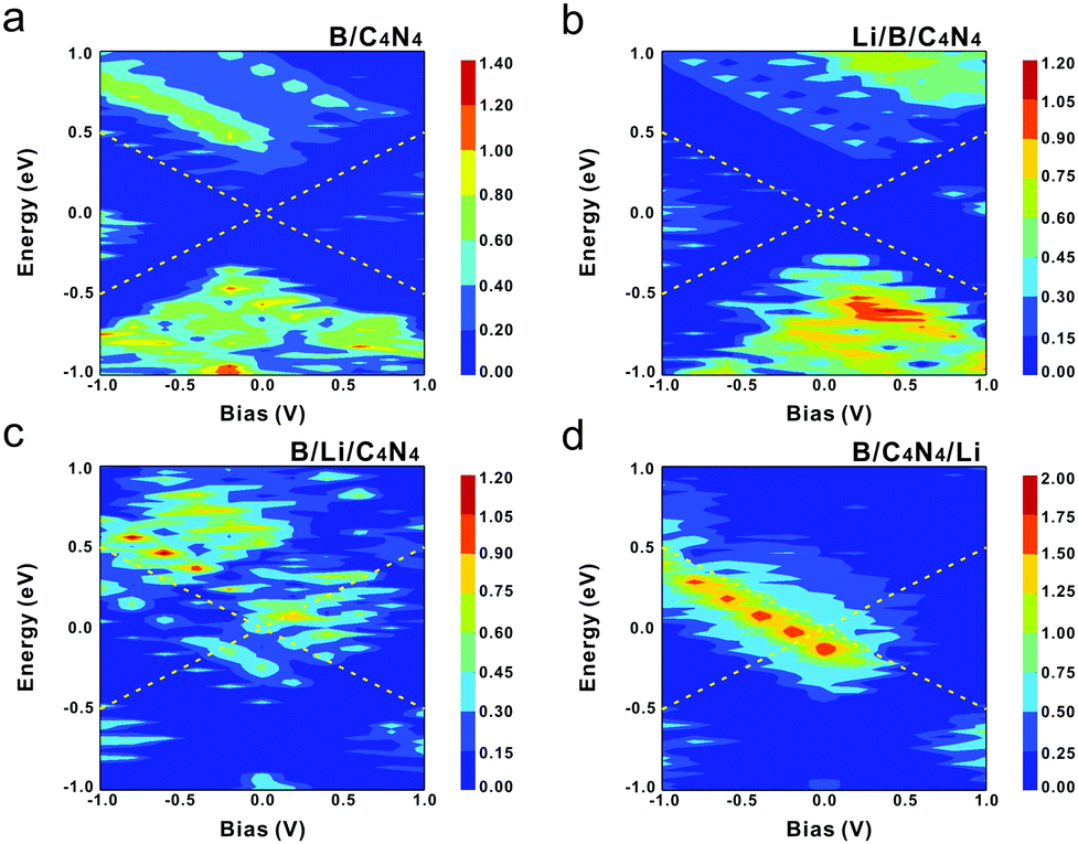 | ||
| Fig. 9 The transmission coefficient contours as a function of energy and bias voltage in (a) B/C4N4, (b) Li/B/C4N4, (c) B/Li/C4N4, and (d) B/C4N4/Li vdW heterojunctions, respectively. The region within the yellow dashed lines is the bias window. | ||
To further analyze why B/C4N4/Li vdW heterojunctions have superior negative rectification behavior, its transport probability at Vb = −1.0 V is compared with that at Vb = 1.0 V. The projected local density of states (PLDOS) and spectral current of B/C4N4/Li vdW heterojunctions at Vb = −1.0 and 1.0 V are displayed in Fig. 10. In PLDOS, the bright block stands for the existence of DOS, whereas the dark one indicates the energy gap without DOS distribution. Borophene and C4N4/Li monolayers are separated by B/C4N4/Li vdW heterojunctions, as indicated by the green vertical line. It is worth noting that the current in B/C4N4/Li is mainly attributed to the transport behavior in the energy region higher than 0 eV, whether at −1.0 V or at 1.0 V. Nevertheless, the transport processes at Vb = −1.0 V and Vb = 1.0 V are quite different. Vb = −1.0 V implies a higher potential of the right C4N4/Li electrode, whereas Vb = 1.0 V means a higher potential of the left borophene electrode. At Vb = −1.0 V, CBM and VBM of the right C4N4/Li electrode are shifted upward relative to EF and CBM of the left borophene electrode. The higher energy levels on the right C4N4/Li with respect to the left borophene provide enough channels for electrons to transport through B/C4N4/Li, as the current under negative bias starts to flow only after VBM of the right electrode reaches CBM of the left one.72 The n-type Ohmic contact in the central B/C4N4/Li vdW heterojunction has no blocking effect on the transport efficiency. Numerous electrons are injected from the adsorbed Li-ions to the C4N4 monolayer, which plays the role of the majority carriers and promotes the interband tunneling from VBM of C4N4/Li to CBM of borophene, thereby resulting in a large reverse current at Vb = −1.0 V. The electron-withdrawing capability of bottom C4N4 in B/C4N4/Li is so strong that it can not only accept electrons from Li-ions but also from upper borophene. As a result, VBM of borophene is occupied by holes, which play as the majority carriers under the forward bias. At Vb = 1.0 V, the higher potential of the left borophene electrode has significantly shifted the CBM and VBM of borophene upward to higher than the EF and CBM of the right C4N4/Li. Consequently, the holes on VBM of the left borophene move to CBM of the right C4N4/Li with relatively low energy, bringing about the forward current. In comparison with the high electron concentration in C4N4/Li, the lower hole concentration in borophene has suppressed the forward current. Therefore, the large difference in carrier concentrations on the upper borophene and bottom C4N4/Li layers of B/C4N4/Li vdW heterojunctions is the origin of its high interlayer tunneling barrier, on which superior negative rectification behavior is generated. This will be of great importance to the application of B/C4N4/Li vdW heterojunctions in high-performance optoelectronic devices, such as photodetectors and photodiodes.
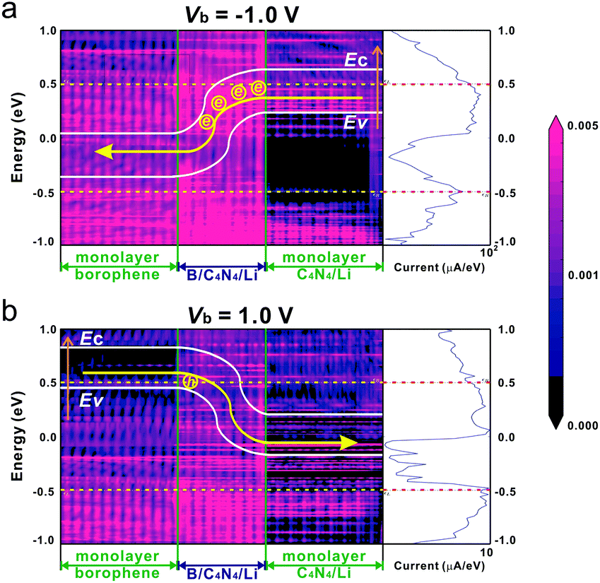 | ||
| Fig. 10 Spatially resolved local density of states (LDOS) (left side) and the corresponding spectral current (right side) in B/C4N4/Li vdW heterojunctions at (a) Vb = −1.0 V and (b) Vb = 1.0 V, respectively. | ||
4. Conclusions
In conclusion, we have developed a new strategy to eliminate the interlayer Schottky barrier in B/C4N4 vdW heterojunctions and finally realized the Ohmic contact between borophene and C4N4, through the combination of vertical stacking and Li-ion adsorption. The remarkable separation of hole–electron pairs in B/C4N4 vdW heterojunctions makes it superior to B/B and C4N4/C4N4 vdW heterojunctions as the candidate structure for photodiode application. The adsorption of Li-ions on B/C4N4 vdW heterojunctions can not only eliminate the Schottky barrier but also increase the tunneling barrier by modulating the adsorption site from top to bottom, achieving an n-type Ohmic contact, which is largely attributed to the enhanced electron injection into the C4N4 sublayer. B/C4N4/Li exhibits the most excellent absorbing capability of the infrared illumination and the strongest negative rectification, among a series of Li-adsorbed B/C4N4 vdW heterojunctions, showing great potential in tunneling photodiode applications. Both the transmission spectra and PLDOS demonstrate that the largest difference in carrier concentrations on the left and right electrodes is the origin of the highest tunneling barrier in the two-probe B/C4N4/Li system at reverse and forward bias, thus resulting in the largest rectifying ratio. Our study is expected to encourage experimental realization of the tunneling photodiode based on vdW heterojunction with Ohmic contact.Author contributions
Cancan Zheng, Man Shi, Haiyan Li, Nianxi Dou, and Zhihao Ma: Data curation; Cong Zhou: Validation; FeiFei Xia: Visualization; Yuanyuan He: Conceptualization, investigation, and writing original draft; Jianwei Zhao: Methodology, software, and supervision.Conflicts of interest
There are no conflicts to declare.Acknowledgements
This work was supported by the National Natural Science Foundation of China (Grant No. 51802121, and 51861145202), Jiaxing Science and Technology Project (Grant No. 2020AY10008, and 2020AD10017), the Student Research Training Program of Jiaxing University (CD8517203297), and the Open Project Program of Key Laboratory of Yarn Materials Forming and Composite Processing Technology, Zhejiang Province, Jiaxing University (MTC2020-17).References
- C. Y.-P. Chao, S.-F. Yeh, M.-H. Wu, K.-Y. Chou, T. Honyih, C.-L. Lee, C. Yin, P. Paillet and V. Goiffon, Sensors, 2019, 19, 5447 CrossRef.
- Z. Liu, S. Li, Z. Y. Yan, Y. Y. Liu, Y. S. Zhi, X. Wang, Z. P. Wu, P. G. Li and W. H. Tang, J. Mater. Chem. C, 2020, 8, 5071–5081 RSC.
- P. E. Malinowski, E. Georgitzikis, J. Maes, I. Vamvaka, F. Frazzica, J. Van Olmen, P. De Moor, P. Heremans, Z. Hens and D. Cheyns, Sensors, 2017, 17, 2867 CrossRef PubMed.
- W. Chen, B. Chen, A. Holmes and P. Fay, Electron. Lett., 2015, 51, 1439–1440 CrossRef CAS.
- M. Mazzillo, G. Condorelli, M. E. Castagna, G. Catania, A. Sciuto, F. Roccaforte and V. Raineri, IEEE Photonics Technol. Lett., 2009, 21, 1782–1784 CAS.
- B. Jeon, H. Lee, K. C. Goddeti and J. Y. Park, ACS Appl. Mater. Interfaces, 2019, 11, 15152–15159 CrossRef CAS PubMed.
- J. Y. Xu, J. S. Yu, J. H. Liao, X. B. Yang, C. Y. Wu, Y. Wang, L. Wang, C. Xie and L. B. Luo, ACS Appl. Mater. Interfaces, 2019, 11, 21702–21710 CrossRef CAS PubMed.
- L. H. Zeng, M. Z. Wang, H. Hu, B. Nie, Y. Q. Yu, C. Y. Wu, L. Wang, J. G. Hu, C. Xie, F. X. Liang and L. B. Luo, ACS Appl. Mater. Interfaces, 2013, 5, 9362–9366 CrossRef CAS PubMed.
- B. Mukherjee, A. Zulkefli, R. Hayakawa, Y. Wakayama and S. Nakaharai, ACS Photonics, 2019, 6, 2277–2286 CrossRef CAS.
- A. Allain, J. H. Kang, K. Banerjee and A. Kis, Nat. Mater., 2015, 14, 1195–1205 CrossRef CAS.
- M. Buscema, J. O. Island, D. J. Groenendijk, S. I. Blanter, G. A. Steele, H. S. J. van der Zant and A. Castellanos-Gomez, Chem. Soc. Rev., 2015, 44, 3691–3718 RSC.
- X. Zhou, X. Z. Hu, S. S. Zhou, H. Y. Song, Q. Zhang, L. J. Pi, L. Li, H. Q. Li, J. T. Lu and T. Y. Zhai, Adv. Mater., 2018, 30, 1703286 CrossRef.
- T. T. Li, C. He and W. X. Zhang, J. Mater. Chem. A, 2019, 7, 4134–4144 RSC.
- R. Longuinhos and J. Ribeiro-Soares, Physica E, 2020, 119, 114007 CrossRef CAS.
- S. W. Yang, W. Li, C. C. Ye, G. Wang, H. Tian, C. Zhu, P. He, G. Q. Ding, X. M. Xie, Y. Liu, Y. Lifshitz, S. T. Lee, Z. H. Kang and M. H. Jiang, Adv. Mater., 2017, 29, 1605625 CrossRef PubMed.
- Y. W. Li, S. H. Zhang, J. B. Yu, Q. Wang, Q. Sun and P. R. Jena, Nano Res., 2015, 8, 2901–2912 CrossRef CAS.
- J. Mahmood, E. K. Lee, M. Jung, D. Shin, I. Y. Jeon, S. M. Jung, H. J. Choi, J. M. Seo, S. Y. Bae, S. D. Sohn, N. Park, J. H. Oh, H. J. Shin and J. B. Baek, Nat. Commun., 2015, 6, 6486 CrossRef CAS PubMed.
- J. Li, C. Cao, J. Hao, H. Qiu, Y. Xu and H. Zhu, Diamond Relat. Mater., 2006, 15, 1593–1600 CrossRef CAS.
- L. Z. Liu, S. J. Xiong and X. L. Wu, Appl. Phys. Lett., 2016, 109, 061601 CrossRef.
- D. Yin and Y. Yoon, J. Appl. Phys., 2016, 119, 214312 CrossRef.
- M. L. Geier, K. Moudgil, S. Barlow, S. R. Marder and M. C. Hersam, Nano Lett., 2016, 16, 4329–4334 CrossRef CAS PubMed.
- S. D. Lei, X. F. Wang, B. Li, J. H. Kang, Y. M. He, A. George, L. H. Ge, Y. J. Gong, P. Dong, Z. H. Jin, G. Brunetto, W. B. Chen, Z. T. Lin, R. Baines, D. S. Galvao, J. Lou, E. Barrera, K. Banerjee, R. Vajtai and P. Ajayan, Nat. Nanotechnol., 2016, 11, 465–471 CrossRef CAS.
- Y. Y. He, F. F. Xia, Z. B. Shao, J. W. Zhao and J. S. Jie, J. Phys. Chem. Lett., 2015, 6, 4701–4710 CrossRef CAS.
- Y. H. Li, Y. A. Deng, J. F. Zhang, Y. Y. Shen, X. Y. Yang and W. W. Zhang, J. Alloys Compd., 2020, 842, 155985 CrossRef CAS.
- Y. C. Huang, D. M. Zhou, X. Chen, H. Liu, C. Wang and S. F. Wang, ChemPhysChem, 2016, 17, 375–379 CrossRef CAS PubMed.
- S. Susarla, V. Kochat, A. Kutana, J. A. Hachtel, J. C. Idrobo, R. Vajtai, B. I. Yakobson, C. S. Tiwary and P. M. Ajayan, Chem. Mater, 2017, 29, 7431–7439 CrossRef CAS.
- L. Nguyen, H. P. Komsa, E. Khestanova, R. J. Kashtiban, J. J. P. Peters, S. Lawlor, A. M. Sanchez, J. Sloan, R. V. Gorbachev, I. V. Grigorieva, A. V. Krasheninnikov and S. J. Haigh, ACS Nano, 2017, 11, 2894–2904 CrossRef CAS PubMed.
- T. Liu, S. Liu, K. H. Tu, H. Schmidt, L. Q. Chu, D. Xiang, J. Martin, G. Eda, C. A. Ross and S. Garaj, Nat. Nanotechnol., 2019, 14, 223–226 CrossRef CAS PubMed.
- Y. Zhang, C. H. Liu, J. B. Liu, J. Xiong, J. Y. Liu, K. Zhang, Y. D. Liu, M. Z. Peng, A. F. Yu, A. H. Zhang, Y. Zhang, Z. W. Wang, J. Y. Zhai and Z. L. Wang, ACS Appl. Mater. Interfaces, 2016, 8, 1381–1387 CrossRef CAS PubMed.
- M. Ke, N. Huu Duy, H. Fan, M. Li, H. Wu and Y. Hu, Nano Res., 2020, 13, 1369–1375 CrossRef CAS.
- Z. Jia, J. Shi, Q. Shang, W. Du, X. Shan, B. Ge, J. Li, X. Sui, Y. Zhong, Q. Wang, L. Bao, Q. Zhang and X. Liu, ACS Appl. Mater. Interfaces, 2019, 11, 20566–20573 CrossRef CAS PubMed.
- Y. Ou, Z. Kang, Q. L. Liao, S. H. Gao, Z. Zhang and Y. Zhang, Nanoscale, 2020, 12, 9859–9865 RSC.
- X. K. Zhang, Q. L. Liao, Z. Kang, B. S. Liu, Y. Ou, J. L. Du, J. K. Xiao, L. Gao, H. Y. Shan, Y. Luo, Z. Y. Fang, P. D. Wang, Z. Sun, Z. Zhang and Y. Zhang, ACS Nano, 2019, 13, 3280–3291 CrossRef CAS PubMed.
- M. Brandbyge, J. L. Mozos, P. Ordejon, J. Taylor and K. Stokbro, Phys. Rev. B: Condens. Matter Mater. Phys., 2002, 65, 165401 CrossRef.
- C. Riplinger and F. Neese, J. Chem. Phys., 2013, 138, 034106 CrossRef PubMed.
- S. Grimme, J. Antony, S. Ehrlich and H. Krieg, J. Chem. Phys., 2010, 132, 154104 CrossRef PubMed.
- M. Schlipf and F. Gygi, Comput. Phys. Commun., 2015, 196, 36–44 CrossRef CAS.
- L. G. Ferreira, M. Marques and L. K. Teles, Phys. Rev. B, 2008, 78, 125116 CrossRef.
- L. G. Ferreira, M. Marques and L. K. Teles, AIP Adv., 2011, 1, 032119 CrossRef.
- R. Landauer, IBM J. Res. Dev., 1988, 32, 306–316 Search PubMed.
- M. Büttiker, Phys. Rev. Lett., 1986, 57, 1761–1764 CrossRef.
- N. A. Vinogradov, A. Lyalin, T. Taketsugu, A. S. Vinogradov and A. Preobrajenski, ACS Nano, 2019, 13, 14511–14518 CrossRef CAS PubMed.
- V. Bezugly, J. Kunstmann, B. Grundkotter-Stock, T. Frauenheim, T. Niehaus and G. Cuniberti, ACS Nano, 2011, 5, 4997–5005 CrossRef CAS.
- D. Liu and D. Tomanek, Nano Lett., 2019, 19, 1359–1365 CrossRef PubMed.
- J. H. Yan, X. Y. Zhang, Y. Y. Pan, J. Z. Li, B. W. Shi, S. Q. Liu, J. Yang, Z. G. Song, H. Zhang, M. Ye, R. G. Quhe, Y. Y. Wang, J. B. Yang, F. Pan and J. Lu, J. Mater. Chem. C, 2018, 6, 6153–6163 RSC.
- M. Yousaf, Y. S. Wang, Y. J. Chen, Z. P. Wang, A. Firdous, Z. Ali, N. Mahmood, R. Q. Zou, S. J. Guo and R. P. S. Han, Adv. Energy Mater., 2019, 9, 1900567 CrossRef.
- Y. F. Li, Y. L. Liang, F. C. R. Hernandez, H. D. Yoo, Q. Y. An and Y. Yao, Nano Energy, 2015, 15, 453–461 CrossRef CAS.
- J. M. Liao, B. S. Sa, J. Zhou, R. Ahuja and Z. M. Sun, J. Phys. Chem. C, 2014, 118, 17594–17599 CrossRef CAS.
- X. Li, W. Liu, B. Huang, H. Liu and X. Li, J. Mater. Chem. C, 2020, 8, 15804–15815 RSC.
- R. Moradian, M. Shahrokhi, S. S. Charganeh and S. Moradian, Physica E, 2012, 46, 182–188 CrossRef CAS.
- H. Guo, Z. Zhang, B. Huang, X. Wang, H. Niu, Y. Guo, B. Li, R. Zheng and H. Wu, Nanoscale, 2020, 12, 20025–20032 RSC.
- X. G. Ma, J. S. Hu, H. He, S. J. Dong, C. Y. Huang and X. B. Chen, ACS Appl. Nano Mater., 2018, 1, 5507–5515 CrossRef CAS.
- V. Shukla, J. Wärnå, N. K. Jena, A. Grigoriev and R. Ahuja, J. Phys. Chem. C, 2017, 121, 26869–26876 CrossRef CAS.
- F. F. Xia, S. Y. Xiong, Y. Y. He, Z. B. Shao, X. J. Zhang and J. S. Jie, J. Phys. Chem. C, 2017, 121, 19530–19537 CrossRef CAS.
- Z. Wang, Y. Zhang, X. Wei, T. T. Guo, J. B. Fan, L. Ni, Y. J. Weng, Z. D. Zha, J. Liu, Y. Tian, T. Li and D. Li, Phys. Chem. Chem. Phys., 2020, 22, 9647–9655 RSC.
- H. M. Hu, Z. Zhang and G. Ouyang, Appl. Surf. Sci., 2020, 517, 146168 CrossRef CAS.
- Y. G. Guo, W. A. Saidi and Q. Wang, 2D Mater., 2017, 4, 035009 CrossRef.
- C. C. Jia, W. Ma, C. H. Gu, H. L. Chen, H. M. Yu, X. X. Li, F. Zhang, L. Gu, A. D. Xia, X. Y. Hou, S. Meng and X. F. Guo, Nano Lett., 2016, 16, 3600–3606 CrossRef CAS.
- R. Oshima, Y. Shoji, K. Makita, A. Ubukata and T. Sugaya, IEEE J. Photovoltaics, 2020, 10, 749–753 Search PubMed.
- S. M. Lu, X. Guan, X. C. Li, J. Liu, F. Huang and W. C. H. Choy, Nano Energy, 2016, 21, 123–132 CrossRef CAS.
- J. B. Wu, H. Y. Chen, N. Yang, J. Cao, X. D. Yan, F. X. Liu, Q. B. Sun, X. Ling, J. Guo and H. Wang, Nat. Electron., 2020, 3, 466–472 CrossRef CAS.
- T. M. Abdolkader, A. Shaker and A. N. M. Alahmadi, Eur. J. Phys., 2018, 39, 045402 CrossRef.
- Y. Y. He, C. Chen, N. Cheng, S. Y. Xiong and J. W. Zhao, Sci. China: Technol. Sci., 2019, 62, 478–489 CrossRef CAS.
- J. W. Zhao, N. Cheng and Y. Y. He, Phys. Chem. Chem. Phys., 2019, 21, 19567–19574 RSC.
- L. Esaki, IEEE Trans. Electron Devices, 1976, 23, 644–647 CrossRef.
- K. Kobashi, R. Hayakawa, T. Chikyow and Y. Wakayama, Adv. Electron. Mater., 2017, 3, 1700106 CrossRef.
- L. Wang, J. M. L. Figueiredo, C. N. Ironside and E. Wasige, IEEE T. Electron. Dev, 2011, 58, 343–347 Search PubMed.
- Y. Wakayama and R. Hayakawa, Adv. Funct. Mater., 2020, 30, 1903724 CrossRef CAS.
- F. Wu, H. Xia, H. D. Sun, J. W. Zhang, F. Gong, Z. Wang, L. Chen, P. Wang, M. S. Long, X. Wu, J. L. Wang, W. C. Ren, X. S. Chen, W. Lu and W. D. Hu, Adv. Funct. Mater., 2019, 29, 1900314 CrossRef.
- J. Singh, R. G. Singh, S. K. Gautam and F. Singh, J. Appl. Phys., 2018, 123, 174503 CrossRef.
- A. Echresh, M. Echresh, V. Khranoyskyy, O. Nur and M. Willander, J. Lumin., 2016, 178, 324–330 CrossRef CAS.
- Y. Y. He, N. Cheng, C. Chen, S. Y. Xiong and J. W. Zhao, Sci. China-Technol. Sci, 2019, 62, 799–810 CrossRef CAS.
Footnote |
| † Electronic supplementary information (ESI) available: Optimized geometries and electronic properties of Li-ion-adsorbed borophene and C4N4 monolayers. See DOI: 10.1039/d0tc05943a |
| This journal is © The Royal Society of Chemistry 2021 |