
 Open Access Article
 This Open Access Article is licensed under a Creative Commons Attribution-Non Commercial 3.0 Unported Licence
Route to tunable room temperature electric polarization in SrTiO3–CoFe2O4 heterostructures†‡
Laura
Maurel
*ab,
Javier
Herrero-Martín
 c,
Federico
Motti
ab,
Hari Babu
Vasili
c,
Cinthia
Piamonteze
b,
Laura J.
Heyderman
ab and
Valerio
Scagnoli
*ab
c,
Federico
Motti
ab,
Hari Babu
Vasili
c,
Cinthia
Piamonteze
b,
Laura J.
Heyderman
ab and
Valerio
Scagnoli
*ab
aLaboratory for Mesoscopic Systems, Department of Materials, ETH Zurich, 8093 Zurich, Switzerland. E-mail: laura.maurel.v@gmail.com; valerios@ethz.ch
bPaul Scherrer Institute, 5232 Villigen PSI, Switzerland
cALBA Synchrotron Light Source, 08290 Cerdanyola del Vallès, Barcelona, Spain
First published on 26th April 2021
Abstract
Utilizing the magnetostrictive properties of CoFe2O4, we demonstrate reversible room temperature control of the Ti electronic structure in SrTiO3–CoFe2O4 heterostructures, by inducing local and reversible strain in the SrTiO3. By means of X-ray absorption spectroscopy, we have ascertained the changes that take place in the energy levels of the Ti 3d orbitals under the influence of an external magnetic field. The observed Ti electronic state when the sample is subjected to moderately large external magnetic fields and the disappearance of the induced phase upon their removal indicates lattice distortions that are suggestive of the development of a net electric polarization.
Introduction
Strain engineering of thin-film heterostructures is one of the most widespread and successful approaches to improving the performance of devices such as transistors,1 electrochemical energy conversion devices,2 or multiferroic (MF) memories.3 Such an approach has enabled researchers to tailor the physical behavior of complex oxides, resulting in strikingly different properties from those of their bulk counterparts.4 Strain engineering is particularly suitable for application to materials presenting incipient phenomena. For instance, SrTiO3 (STO) provides a textbook example of a so-called quantum paraelectric (QPE) phase5 in which, due to quantum fluctuations, the ferroelectric (FE) domain correlation lengths do not extend beyond nanometer length scales.6 Such subtle equilibria can be altered with external stimuli, inducing long-range ferroelectricity. In addition, the artificial interfaces created within STO-oxide heterostructures are likely to promote the stabilisation of FE order and therefore these systems have provided a fertile playground in the search for novel functional devices. In particular, the engineering of STO-oxide bilayer heterostructures has given rise to a variety of interfacial properties,7 such as interface conductivity,8,9 magnetic order,10 superconductivity11 and polar vortices.12 The emergence of some of these interfacial properties has been explained by the presence of FE order in STO. For example, the direction of the spontaneous polarization plays a crucial role in the critical thickness required to stabilize a two dimensional electron gas.13 Therefore, these novel interfacial properties are very sensitive to the STO FE polarization state. Such FE order in STO is promoted by increasing the unit cell volume, which favours the hybridization of filled O 2p-orbitals with empty Ti 3d-orbitals, leading to the formation of a strong covalent bond.14 Given the prospects of exploiting the resulting FE polarization in devices, many approaches have been utilized to achieve FE order, which rely on the application of stress,15,16 strain,17,18 cation substitution,19,20 or cation defects such as Sr-vacancies21–23 and antisite Ti/Sr defects.24 However, any practical use of such functional materials is hindered by the fact that, after their growth, the induced ferroelectricity in STO cannot be manipulated.Here, we demonstrate reversible control of the Ti electronic structure at room temperature in CoFe2O4–SrTiO3 (CFO-STO) heterostructures in the presence of an applied magnetic field suggestive of the development of net electric polarization. Our approach is based on the following strategy: first, we need to suppress quantum fluctuation in STO so that it can develop a net electric polarization or a FE polarization22 and, secondly, we want to be able to control the net electric polarization or the FE state using an externally applied stimulus at room temperature. A tunable external magnetic field was chosen for this purpose. Both of these concepts are realized with the deposition of a specific two-phase self-assembled CFO-STO heterostructure. Here, we increase the likelihood of STO becoming FE by introducing and tuning the Sr deficiency of the film. This control of Sr stoichiometry during the STO growth was shown to stabilize FE order in the material.21,22 The possibility to stabilize and control the lattice distortion with the possible development of an associated electric polarization with an external magnetic field was achieved by an efficient elastic coupling of STO with CFO that has large magnetostriction coefficient. Specifically, the application of an external magnetic field, which modifies the volume and shape of CFO, results in a local reversible strain in STO. This local strain in turn induces a distortion in the STO structure. However, it should be noted that magnetostriction alone might be insufficient to develop a FE order in STO at room temperature. It is, therefore, crucial to increase the number of defects in the material, by controlling the Sr deficiency, as this directly influences the degree of covalency in STO. In summary, the combination of Sr deficiency and a magnetic field perturbation enables us to maximize the effect of the magnetic field to reversibly modify the Ti 3d-orbital level arrangement and Ti-O covalency in STO at room temperature.
Experimental
Sample preparation
CoFe2O4–SrTiO3 films were deposited by pulsed laser deposition on (001)-oriented SrTiO3 substrates from a target consisting of 1/3 CoFe2O4 and 2/3 SrTiO3. A Coherent KrF laser (λ = 248 nm) was used for the ablation with 1 J cm−2 energy and 2 Hz repetition rate. The oxygen pressure was kept at 6.66 mbar during sample deposition. After deposition, the samples were annealed at full oxygen pressure for 30 minutes at the respective growth temperatures and, maintaining full oxygen pressure, cooled down at 10° per minute to room temperature. Initially, samples were deposited at different temperatures as discussed in the ESI‡ (Fig. S1). XAS characterization was performed on samples grown at nominally 800 °C.Laboratory-based sample characterization
Magnetic characterization was performed at 300 K in a SQUID MPMS3 magnetometer (Quantum Design) along the in-plane and out of plane direction of the films. The diffraction characterization was performed in a D8 Discovery microsource diffractometer from Bruker equipped with a 1D detector, with X-ray wavelength λ corresponding to the Cu Kα line (λ = 1.54 Å).Soft X-ray absorption spectroscopy
X-ray absorption spectroscopy (XAS) and X-ray linear dichroism (XLD) measurements were performed at beamline BL29-BOREAS25 of the ALBA Synchrotron (Barcelona, Spain) across the Ti L2,3 edges in total-electron-yield (TEY) detection mode under ultrahigh vacuum conditions (2 × 10⁻¹⁰ mbar). XLD measurements were obtained by subtracting normalized XAS spectra recorded using horizontal linearly polarized X-rays from those acquired using vertically polarized X-rays. All XLD spectra were obtained from averages over at least three octets (a group of four XAS spectra taken for each of the two X-ray polarization directions in an alternate sequence that minimizes eventual, undesired systematic errors with time). All measurements were consistent with Ti ions in a tetravalent oxidation state. The eventual presence of Ti3+ cations could be discarded because of the absence of any additional spectral features at 459 eV and of any X-ray magnetic circular dichroism (XMCD) signal at low temperature (not shown).26Analysis of the XLD spectrum
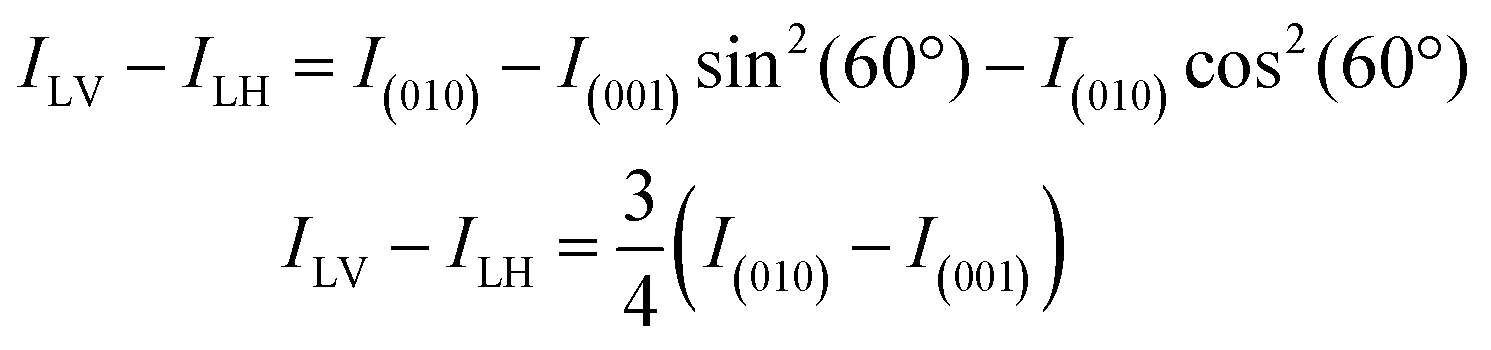
The Ti XLD signal was measured at normal incidence and grazing incidence (60° with respect to normal incidence) geometries. The average of a set of three “octets” were used for each curve. The spectra were normalized at the Ti L2eg peak after subtraction of a linear background. The normalized absorption XASN is given by the expression XASN = (XAS − XASmin)/(XASmax* − XASmin), where XASmax* is the maximum intensity of the XAS spectra in the energy range 464–470 eV corresponding to the L2 edge. We used the same procedure applied in ref. 26 to estimate the X-ray linear dichroism. In normal incidence, the XLD was calculated by taking the difference between the SrTiO3 XAS spectra recorded with the vertical and horizontal electric polarization vector of the incoming beam. For this experimental geometry (see also Fig. S3, ESI‡), the (100) sample crystallographic direction is probed for linear horizontal (LH) and the (010) direction is probed for linear vertical (LV) polarized light. For the experiments performed while a magnetic field is applied along the (100) direction, the XLD spectrum was calculated after subtracting XAS(100)–XAS(010), which is the difference between the spectra measured with the light polarization vector along the long and short axes of SrTiO3 in the strained film. In grazing incidence, the sample was rotated 60° with respect to the surface normal. X-ray photons with LV polarization are kept parallel to the (010) direction while, with LH polarization, the X-ray propagation direction form an angle of 60° with the (100) direction and of 30° with the (001) direction. Assuming that the difference of the XAS spectra measured along the (100) and (010) directions is negligible, the linear dichroism can be calculated as follows:
where E is the electric field vector and I ∝ E2 is the measured absorption.
Simulations
Charge-transfer multiplet calculations were performed with the CTM4XAS software package.27,28 The results of the XAS and XMCD spectra calculations are used to extract quantitative information on the electronic state of the Ti ions. For further details, please see the ESI.‡Results and discussions
Crystal, structural and magnetic behavior of the films
In order to create and control uncompensated electric dipoles in STO, and eventually ferroelectricity, the sample growth parameters need to be carefully controlled. Indeed, we have found that the deposition temperature strongly influences the number of Sr vacancies present in the samples. This is particularly important as the presence of Sr vacancies in STO films is essential to obtain a net electric polarization.21,22With the goal to induce and control ferroelectricity in our heterostructures, we co-deposited magnetostrictive CoFe2O4 and SrTiO3. The preferential growth and the separation of the two constituents results from the different surface energy anisotropy between both materials.29 The lowest energy surface in a structure, {111} in CFO with spinel structure, and {001} in STO with perovskite structure, defines the preferential growth mode of the material deposited. On a (001)-oriented perovskite substrate such as STO, spinels tend to nucleate and form islands, whereas perovskites wet the substrate. This behavior allows us to grow CFO nanocolumns embedded within an STO matrix, an arrangement that notably enhances the elastic coupling between these two materials.
We fabricated a 60 nm thick STO-CFO sample by pulsed laser deposition. The growth temperature of the film was set to 800 °C. After the growth, the crystal structure of the samples was determined by X-ray diffraction (XRD) measurements. The STO and CFO phases have an in-plane (100) crystallographic orientation aligned along the in-plane (100) direction of the substrate (Fig. S1b, ESI‡). XRD results (Fig. 1a) reflect the high degree of crystallographic ordering of the two constituents of the heterostructure with no intermixing between them. Films deposited at all temperatures presented a (001) out-of-plane texture (Fig. S1a, ESI‡). The presence of an out-of-plane texture is indicated by the position of the film Bragg peak reflecting a lattice expansion of the unit cell above the nominal STO lattice constant value ap = 3.905 Å.30 In thin films, this lattice expansion produces an increase of the out-of-plane lattice parameter c while the in-plane lattice parameter a remains the same as that of the STO substrate because of epitaxy. A correlation between the increase in the unit cell tetragonality c/a and the appearance of SrO vacancies in the films has been reported in ref. 21 and 22. We can therefore assume that our tetragonal film incorporates a certain amount of Sr vacancies.
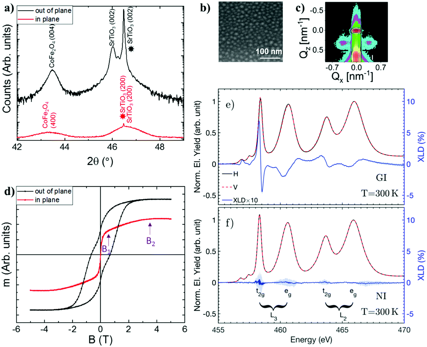 | ||
| Fig. 1 Sample characterization at room temperature. (a) X-ray diffraction 2θ scan measured along the out of plane (black line) and in-plane (red line) directions of the sample. The star indicates the position of the Bragg 2θ angle for the lattice parameter of the (001)-oriented SrTiO3 substrate. The constituent for each peak, together with its index, is indicated on top of each peak. (b) Scanning electron microscopy image of a representative part of the sample. (c) GISAXS map measured at 0.6° incidence angle. (d) Hysteresis loop measured along the in-plane (red) and out of plane (black) direction of the film. B1 and B2 indicate, respectively, the values of the magnetic field at the inflection point, and the value after which the magnetization remains constant. (e) XAS spectra measured in grazing incidence (GI) (red and black) and (f) normal incidence (NI). The detailed geometry for each of the measurements is illustrated in the ESI.‡ In blue, the XLD spectra obtained for both geometries multiplied by 10. Blue shading indicates errorbars associated with the measurements. | ||
The film lattice parameters were obtained by analyzing the in-plane and out-of-plane 2θ-scans shown in Fig. 1a and Fig. S1 (ESI‡). The STO out-of-plane lattice parameter 3.9408(2) Å implies 0.92% lattice expansion with respect to the 3.905 Å lattice parameter in bulk and c/a = 1.009. Therefore, our film has a unit cell with a tetragonal distortion close to that of bulk BaTiO3 in the tetragonal phase,26 with c/a = 1.011.
The size and distribution of the CFO nanocolumns within the STO matrix were first determined by scanning and transmission electron microscopy (SEM and STEM, respectively). An illustrative image of our sample is shown in Fig. 1b, where the columns (light contrast) have an average radius of 15 ± 5 nm and a similar average periodicity. The TEM cross section shows that the columns span all the film thickness (see Fig. S2, ESI‡). To determine the distribution of the nanocolumns in the heterostructure across the whole film, Grazing-Incidence Small Angle X-ray Scattering (GISAXS) maps were recorded under different X-ray incidence angle conditions. A clear GISAXS pattern appeared at 0.6° incidence angle (Fig. 1c), well above the critical angle. Beyond this angular value, the X-ray beam penetrated the whole film indicating that the CFO nanocolumns form a well ordered lattice in the STO matrix throughout the whole thickness of the sample. The analysis of the GISAXS patterns presented in Fig. 1c was performed following the approach presented in ref. 31. The most prominent feature in the observed GISAXS patterns is a side peak occurring at larger scattering angles. The peak reflects the presence of a maximum in the interference function describing the column-to-column correlation distance. The average lattice periodicity D of the columns was inferred from the position of the peak at Qx = ±0.38 nm−1 using the relationship QX ≈ 2π/D. We conclude that the CFO nanocolumns are homogeneous in size and form a lattice with an average period of D = 16.5(5) nm within the STO matrix, which is in agreement with the SEM results.
Finally, the room temperature magnetic properties of our heterostructure with CFO nanocolumns were measured with a magnetometer and the results obtained are shown in Fig. 1d. The magnetization points out-of-plane due to the presence of a strong magnetic anisotropy. A linear extrapolation of the field-dependent magnetization yields an anisotropy field of B2 = 3.5(5)T, which is in agreement with previous results in self-assembled CFO-BTO structures.26,32 Measurements of the magnetization along the in-plane direction show that the magnetization undergoes a sharp increase up to B1 = 0.4(2)T and then it slowly increases until reaching a maximum at B2.
X-ray absorption spectroscopy as a tool to infer the presence of electrical polarization
The direct observation of spontaneous electrical polarization (shortly, FE order) by current-integrating measurements is challenging for our heterostructures because of the difficulties in realizing suitable electrodes for the measurements and the presence of charge losses. Due to the prevalence of such difficulties in FE measurements, we use X-ray absorption spectroscopy (XAS) measurements, which is an alternative contact-free technique to analyze the cationic orbital structure and correlate it with the possible presence of a net electric polarization.4,26 We have determined the Ti 3d-orbital arrangement and occupation as a function of temperature and applied magnetic field. From our measurements, we have determined the presence of lattice distortions suggesting the development of an electrical polarization in the sample. Here, we summarize the main X-ray spectroscopic results obtained, which are discussed in more detail in the following sections.Sr-deficient STO films are expected to behave as FEs,21,22 even in the absence of an applied magnetic field. First, the X-ray absorption spectra from the sample were measured at 300 K and at 50 K. We expect the fingerprints of FE or at least the presence of a net electric polarization to appear or to be more evident at low temperature. We analyzed the effects of the vacancy enhanced Ti-O covalency on the measured XAS spectra. Subsequently, the sample was remeasured at 300 K under an applied magnetic field, demonstrating control of the Ti 3d-orbital splitting in Sr deficient STO upon application of the magnetic field. Moreover, the initial orbital configuration in STO is restored following the removal of the external magnetic field, demonstrating the possibility to reversibly control the SrTiO3 electron structure after sample growth.
Ti 3d orbital rearrangement at 50 K
In this section, we compare the Ti L2,3 XAS spectra at 300 K and 50 K to look for possible X-ray spectroscopic changes ascribed to the reported phase transition, which is known to occur at 105 K in bulk samples33 and possibly to observe the development of a FE component below the phase transition temperature. The use of a contrast synchrotron-based technique such as X-ray linear dichroism (XLD) is ideally suited here as a searchlight to probe empty valence band states with a nonzero projection parallel to the X-ray polarization. XLD is obtained by subtracting two XAS spectra obtained with vertical and horizontal polarization (see the Experimental section for more details). We start by presenting the measurements gathered at 300 K. The XAS and XLD spectra obtained at 300 K for our sample, for grazing incidence and normal incidence geometries in the vicinity of the Ti L2,3 absorption edges, are shown in Fig. 1e and f. Both at the L3 and L2 edges, two main absorption features arise corresponding to electronic transitions from the 2p3/2 and 2p1/2 core levels (for L3 and L2 edges, respectively) towards the lower-energetic dxy, dyz, dxz orbitals (t2g states), and the higher-energetic dz2 and dx2−y2 (eg states). The XLD signal measured in normal incidence is negligible within the experimental error, whereas a well-defined dichroic signal appears in the grazing incidence geometry, as shown in Fig. 1e. The latter signal is not expected for a cubic crystal field, and reflects the sample tetragonality. Indeed, in this geometry, we probe the anisotropy between the inequivalent a and c crystallographic directions.In order to obtain a quantitative determination of the Ti 3d orbital level distribution, charge-transfer multiplet calculations were performed using the CTM4XAS code.27,28 A detailed description of the various parameters used for the simulations can be found in the ESI‡ (see Fig. S4 and S5). The crystal field parameter 10Dq, which determines the energy splitting between the t2g and eg states in a cubic crystal field (see Fig. 2a), is found to be 10Dq = 1.9 eV, in good agreement with previous studies on STO and BTO.26,34–36 When the local symmetry is lowered due to lattice deformations, the t2g and eg states further split and additional parameters, Ds and Dt, are required to correctly account for the further lifting of 3d orbital degeneracy. In this scenario, the best fit for the 300 K experimental data was found by introducing charge transfer effects (details are given below) and for DS = −0.03 eV and Dt = 0.03 eV. These values correspond to a 240 meV splitting of the t2g levels with the dxy orbital lowest in energy, as illustrated in Fig. 2a. We then simulated the expected spectral shape for the XAS measurements performed at 50 K, in order to determine the origin of the differences between the corresponding experimental spectra. Both 300 K and 50 K XLD spectra are shown in Fig. 2c and they allow us to correlate specific spectral changes to the development of orbital polarization in our sample. Qualitatively, a noticeable shift of the X-ray spectral features towards lower energy appears, which corresponds to the electronic transitions to the Ti 3d eg states. To obtain quantitative information of the change in the Ti orbital configuration one should note that, in the presence of FE order, any change in the charge-transfer probability should be observed in the multiplet calculations. Indeed, we have found that the observed XLD spectral changes cannot be described by varying the crystal field parameters 10Dq, Dt and Ds parameters, while keeping the charge-transfer energy fixed to the value found for 300 K. Specifically, varying Dt and Ds, which physically corresponds to a change in the tetragonality of the unit cell, results in sizable changes of the simulated XAS spectra that are not observed in our measurements (see Fig. S4 in the ESI‡).
 | ||
| Fig. 2 (a) Orbital splitting of the Ti4+ ion in octahedral coordination, where the t2g and eg levels are split by an energy 10Dq. When symmetry is reduced in the tetragonal structure, the levels further split into dz2, dx2−y2,dxz/dyz and dxy orbitals, whose energy parametrization in terms of Dq, Dt and Ds, is 6Dq − 2Ds − 6Dt, 6Dq + 2Ds − Dt, −4Dq − Ds + 4Dt and −4Dq + 2Ds − Dt, respectively. (b) XAS (black line) and XLD spectra calculated through charge-transfer multiplet calculations using CTM4XAS with optimal parameters used to match the simulations with the experimental spectra measured in grazing incidence at 300 K (red line) and at 50 K (blue line). (c) XAS spectra measured under grazing incidence (GI) at 50 K, with the associated XLD spectra (dark blue) and the corresponding XLD spectra at 300 K (pink). (d) XAS spectra measured under normal incidence (NI) at 50 K, with the associated XLD spectra (dark blue). | ||
Charge-transfer effects are accounted for by introducing a charge-transfer energy term, Δ, which represents the ionic energy difference between Ti d0 and d1![[L with combining low line]](https://www.rsc.org/images/entities/i_char_004c_0332.gif) configurations, where denotes a hole at the ligand (O in our case) in the initial state, with an electron being transferred to the metal's valence band.37Upd describes the attractive interaction between the core-hole and 3d electrons, and Udd accounts for the on-site electron–electron Coulomb repulsion energy. In our simulations, we have used Upd − Udd = 2 eV and Δ = 3 eV, which are values compatible with those reported for similar materials.34,38 Furthermore, one has to introduce the hopping integral parameters Ti to describe the probability of an electron being transferred from O to Ti. In a tetragonal environment, four parameters must be introduced, Tb1, Ta1, Tb2, Te referring to the hopping into dx2−y2, dz2, dxy and dxz (dyz) orbitals, respectively. Since the 3d levels preserve some degeneracy, it is reasonable to assume that Tb1 = Ta1 and Tb2 = Te, at least for the 300 K case. To describe our experimental results, Tb1 and Tb2 were tuned (see Table 1 and Fig. S4, ESI‡) and we have found that Tb1 > Ta1 is required in order to describe the 50 K experimental data, suggesting an enhancement of in-plane covalency at 50 K with respect to 300 K. We find that a value of Tb2 (Tb1) of 1 eV (2.1 eV) qualitatively reproduces the spectral features shift observed in the 50 K measurements. In general, varying Tb1 has more effect on the XLD than a change in Tb2. From Tb1 > Ta1 we can infer that the increase of covalency in TiO6 octahedra does not occur along the long axis of the perovskite ((001) in our case), as in standard displacive FEs but along the perpendicular direction, as observed in non-stoichiometric films. In such a case, Yang et al. showed that the Ti4+ cation was off-centered along the (111) direction due to a change in its coordination with the neighbouring ions. Therefore, our simulations indicate an increase of the in-plane covalency, which, in turn, could be explained by an off-centering of Ti4+, compatible with the appearance of net electric polarization.
configurations, where denotes a hole at the ligand (O in our case) in the initial state, with an electron being transferred to the metal's valence band.37Upd describes the attractive interaction between the core-hole and 3d electrons, and Udd accounts for the on-site electron–electron Coulomb repulsion energy. In our simulations, we have used Upd − Udd = 2 eV and Δ = 3 eV, which are values compatible with those reported for similar materials.34,38 Furthermore, one has to introduce the hopping integral parameters Ti to describe the probability of an electron being transferred from O to Ti. In a tetragonal environment, four parameters must be introduced, Tb1, Ta1, Tb2, Te referring to the hopping into dx2−y2, dz2, dxy and dxz (dyz) orbitals, respectively. Since the 3d levels preserve some degeneracy, it is reasonable to assume that Tb1 = Ta1 and Tb2 = Te, at least for the 300 K case. To describe our experimental results, Tb1 and Tb2 were tuned (see Table 1 and Fig. S4, ESI‡) and we have found that Tb1 > Ta1 is required in order to describe the 50 K experimental data, suggesting an enhancement of in-plane covalency at 50 K with respect to 300 K. We find that a value of Tb2 (Tb1) of 1 eV (2.1 eV) qualitatively reproduces the spectral features shift observed in the 50 K measurements. In general, varying Tb1 has more effect on the XLD than a change in Tb2. From Tb1 > Ta1 we can infer that the increase of covalency in TiO6 octahedra does not occur along the long axis of the perovskite ((001) in our case), as in standard displacive FEs but along the perpendicular direction, as observed in non-stoichiometric films. In such a case, Yang et al. showed that the Ti4+ cation was off-centered along the (111) direction due to a change in its coordination with the neighbouring ions. Therefore, our simulations indicate an increase of the in-plane covalency, which, in turn, could be explained by an off-centering of Ti4+, compatible with the appearance of net electric polarization.
| Geometry, temperature, magnetic field | Δ | U pd | U dd | T b1 | T a1 | T b2 | T e |
|---|---|---|---|---|---|---|---|
| GI at 300 K, 0 T | 3 | 8 | 6 | 2 | 2 | 1 | 1 |
| GI at 50 K, 0 T | 3 | 8 | 6 | 2.1 | 1.9 | 1 | 1 |
| GI at 300 K, 2 T | 3 | 8 | 6 | 2.1 | 1.9 | 1 | 1 |
Magnetic control of the Ti electron configuration at 300 K
Having characterized the electronic configuration of our STO heterostructure above and below the anti-ferro distortive transition temperature and after settling the fingerprints that are compatible with an induced net electric polarization in XLD spectra, we can now compare these results with those obtained (at 300 K) in the presence of an external magnetic field. We first discuss the anticipated changes in the sample due to the CFO magnetostriction. When the magnetic field is applied along the (100) in-plane direction, the shape of the nanocolumns is expected to distort (Fig. 3a). Due to the negative magnetostriction coefficient, the nanocolumns tend to contract along the direction of the applied magnetic field (λ‖ = −2 × 10⁻⁴ < 0) and to expand along the perpendicular plane (λ⊥ = 10−4 > 0). The net result is the generation of a directional strain in SrTiO3, leading to a symmetry lowering in the film plane (with a(010) > a(100)). The emergence of an anisotropy in the orbital distribution along the (100) and (010) directions is indicated by the appearance of XLD signal at the Ti L3 edge in the normal incidence geometry (see Fig. 3c). | ||
| Fig. 3 (a) Schematic showing CFO nanocolumns within the STO matrix (left) and the effect of magnetostriction after applying a magnetic field (right). (b) Ti L2,3 XAS measured in the grazing incidence (GI) geometry and (c) normal incidence (NI) at 300 K with a 2 T magnetic field applied along the (100) STO axis. The XLD with (blue) and without (pink) the 2 T field are shown for comparison. (d) Room temperature XLD measured in normal incidence geometry at different values of the magnetic field. The pink shading indicates the Ti L3t2g XLD peak where the strongest spectral changes are observed. In the inset, it can be seen that the dependence of the in-plane magnetization (red) and maximum of the Ti L3t2g XLD peak (black dots) as a function of the magnetic field agree well. | ||
We then determined the minimum magnetic field required to induce this in-plane distortion at 300 K by measuring the XLD spectrum for different values of the applied magnetic field (Fig. 3d). Here, we discuss the behavior of the eg peak (pink shading) because of its direct link with the covalency of Ti 3d orbitals. After applying a field of 0.1 T, spectral variations could be seen in the 458–460 eV energy region indicating the onset of an in-plane distortion. These spectral changes increased with the applied field up to 0.4 T but, beyond this value, no further evolution was observed. In order to determine whether there is a correlation between this XLD behaviour and the CFO magnetic properties, we quantified the former and compared them with the sample magnetization. For this, we determined the integrated area AXLD of the selected region of the XLD spectra and its maximum value MXLD as a function of the applied magnetic field. The modelling of the spectra in the aforecommented reduced energy interval around the Ti L3 edge was done using a Voigt profile. The MXLD dependence as a function of the applied magnetic field is compared with the magnetization curve in the inset of Fig. 3d. A similar field dependence indicates a strong correlation between changes in the orbital distribution and magnetization. This is consistent with the fact that we expect a positive correlation between magnetostriction and the applied magnetic field until a saturation value is reached, beyond which the shape of the CFO nanocolumns does not further change. In CFO such a relationship is well characterized and it has been demonstrated that a maximum magnetostrictive effect is achieved at the inflection point (labeled as B1, in Fig. 1d) of the magnetization curve.39 Thus, the correlation between the orbital distribution and magnetization demonstrates that the evolution observed in the Ti L2,3 XLD spectra is the result of the strain generated by the shape modification in CFO nanostructures due to magnetostriction, and that an applied magnetic field of 0.4 T is sufficient to maximize the changes in the energy of Ti 3d-states of our films.
Finally, in order to assert if the modification of the Ti 3d orbital energies are confined to the sample in-plane directions probed in the normal incident geometry, we also discuss the changes in the XLD spectra measured in grazing incidence geometry (Fig. 3b) while applying a magnetic field along the (100) direction. GI measurements allow also to check if the XLD spectroscopic evolution produced by cooling the sample to 50 K is comparable to the changes observed in the presence of an applied external magnetic field. We note here that the coefficients for magnetostriction are ideally identical along the (010) and (001) directions because both are orthogonal to the applied magnetic field, and hence the strain applied to STO. Since the (100) applied field produces a distortion in the atomic orbitals along the (010) and (001) directions, this results in a change in the grazing incidence XLD signal: the amplitude of the spectroscopic features corresponding to the t2g orbitals gets reduced whereas the eg features shift toward lower energies as in the 50 K case. The observed positions of the XAS peaks are nearly identical and therefore the structural changes along the probed directions are minimal.
Summarizing, we have seen that the XLD spectrum changes only because of an enhanced covalence within the film plane. This change, together with the modification of the Ti 3d-states energies along the (100) and (010) directions, suggests the emergence of a net electric polarization component along the (100) direction driven by the applied magnetic field.
Conclusions
We have demonstrated that, by applying an external magnetic field, it is possible to induce and reversibly manipulate the electronic structure of Ti 3d orbitals in Sr-deficient self-assembled STO-CFO heterostructures. This change in the Ti local electronic distribution is probed by synchrotron X-ray absorption spectroscopy and can be explained by a increase in charge transfer in-plane. We argue that this electronic structure change can be explained by the development of electric polarization since this is expected to modify the Ti 3d-O 2p charge transfer probability. Specifically, when applied along the (100) crystal direction, the magnetic field induces a local strain in STO that lowers the crystallographic symmetry in the films, resulting in a measurable XLD signal in normal incidence geometry. This is due to a rearrangement of Ti 3d-orbitals that lowers the energy barrier that Ti cations need to overcome in order to move away from their original position40 and indicates the possible presence of a FE component along the (100) direction. Thus, our novel approach offers an important step towards the reversible modification of the net electric polarization state of STO heterostructures at room temperature. In addition, we can envisage that, since some interfacial functionalities are linked to the STO ferroelectricity, this methodology could be applied to other 2D heterostructures offering the possibility to induce and reversibly control novel properties found at the interface, such as polar vortices or two-dimensional electron gases.Conflicts of interest
There are no conflicts to declare.Acknowledgements
We are grateful to C. Vaz for fruitful discussions and to J. Blasco for preparing the targets used for the pulse laser deposition process. The Swiss National Science Foundation (SNF) is kindly acknowledged for co-funding of the electron microscope (R’Equip Project 206021_177020).References
- G. Tsutsui, S. Mochizuki, N. Loubet, S. W. Bedell and D. K. Sadana, AIP Adv., 2019, 9, 030701, DOI:10.1063/1.5075637.
- B. Yildiz, MRS Bull., 2014, 39, 147–156, DOI:10.1557/mrs.2014.8.
- A. Roy, R. Gupta and A. Garg, Adv. Condensed Matter Phys., 2012, 2012, 926290, DOI:10.1155/2012/926290.
- E. Arenholz, G. van der Laan, A. Fraile-Rodriguez, P. Yu, Q. He and R. Ramesh, Phys. Rev. B: Condens. Matter Mater. Phys., 2010, 82, 140103, DOI:10.1103/PhysRevB.82.140103.
- K. A. Muller and H. Burkard, Phys. Rev. B: Condens. Matter Mater. Phys., 1979, 19, 3593–3602, DOI:10.1103/physrevb.19.3593.
- S. E. Rowley, L. J. Spalek, R. P. Smith, M. P. M. Dean, M. Itoh, J. F. Scott, G. G. Lonzarich and S. S. Saxena, Nat. Phys., 2014, 10, 367–372, DOI:10.1038/Nphys2924.
- Y. Y. Pai, A. Tylan-Tyler, P. Irvin and J. Levy, Rep. Prog. Phys., 2018, 81, 036503, DOI:10.1088/1361-6633/aa892d.
- J. Garcia-Barriocanal, A. Rivera-Calzada, M. Varela, Z. Sefrioui, E. Iborra, C. Leon, S. J. Pennycook and J. Santamaria, Science, 2008, 321, 676–680, DOI:10.1126/science.1156393.
- B. Kalisky, E. M. Spanton, H. Noad, J. R. Kirtley, K. C. Nowack, C. Bell, H. K. Sato, M. Hosoda, Y. W. Xie, Y. Hikita, C. Woltmann, G. Pfanzelt, R. Jany, C. Richter, H. Y. Hwang, J. Mannhart and K. A. Moler, Nat. Mater., 2013, 12, 1091–1095, DOI:10.1038/Nmat3753.
- M. R. Fitzsimmons, N. W. Hengartner, S. Singh, M. Zhernenkov, F. Y. Bruno, J. Santamaria, A. Brinkman, M. Huijben, H. J. A. Molegraaf, J. de la Venta and I. K. Schuller, Phys. Rev. Lett., 2011, 107, 217201, DOI:10.1103/PhysRevLett.107.217201.
- L. Li, C. Richter, J. Mannhart and R. C. Ashoori, Nat. Phys., 2011, 7, 762–766, DOI:10.1038/nphys2080.
- A. K. Yadav, C. T. Nelson, S. L. Hsu, Z. Hong, J. D. Clarkson, C. M. Schlepuetz, A. R. Damodaran, P. Shafer, E. Arenholz, L. R. Dedon, D. Chen, A. Vishwanath, A. M. Minor, L. Q. Chen, J. F. Scott, L. W. Martin and R. Ramesh, Nature, 2016, 530, 198–201, DOI:10.1038/nature16463.
- H. L. Guo, W. A. Saidi and J. Zhao, Phys. Chem. Chem. Phys., 2016, 18, 28474–28484, 10.1039/c6cp04769f.
- M. H. Whangbo, E. E. Gordon, J. L. Bettis, A. Bussmann-Holder and J. Kohler, Z. Anorg. Allg. Chem., 2015, 641, 1043–1052, DOI:10.1002/zaac.201500058.
- H. Uwe and T. Sakudo, Phys. Rev. B: Condens. Matter Mater. Phys., 1976, 13, 271–286, DOI:10.1103/PhysRevB.13.271.
- W. J. Burke and R. J. Pressley, Solid-State Commun., 1971, 9, 191–195, DOI:10.1016/0038-1098(71)90115-3.
- D. G. Schlom, L. Q. Chen, C. B. Eom, K. M. Rabe, S. K. Streiffer and J. M. Triscone, Annu. Rev. Mater. Res., 2007, 37, 589–626, DOI:10.1146/annurev.matsci.37.061206.113016.
- R. J. Xu, J. W. Huang, E. S. Barnard, S. S. Hong, P. Singh, E. K. Wong, T. Jansen, V. Harbola, J. Xiao, B. Y. Wang, S. Crossley, D. Lu, S. Liu and H. Y. Hwang, Nat. Commun., 2020, 11, 3141, DOI:10.1038/s41467-020-16912-3.
- J. G. Bednorz and K. A. Muller, Phys. Rev. Lett., 1984, 52, 2289–2292, DOI:10.1103/PhysRevLett.52.2289.
- T. Mitsui and W. B. Westphal, Phys. Rev., 1961, 124, 1354–1359, DOI:10.1103/PhysRev.124.1354.
- Y. S. Kim, J. Kim, S. J. Moon, W. S. Choi, Y. J. Chang, J. G. Yoon, J. Yu, J. S. Chung and T. W. Noh, Appl. Phys. Lett., 2009, 94, 202906, DOI:10.1063/1.3139767.
- Y. S. Kim, D. J. Kim, T. H. Kim, T. W. Noh, J. S. Choi, B. H. Park and J. G. Yoon, Appl. Phys. Lett., 2007, 91, 042908, DOI:10.1063/1.2764437.
- K. T. Kang, H. I. Seo, O. Kwon, K. Lee, J. S. Bae, M. W. Chu, S. C. Chae, Y. Kim and W. S. Choi, Appl. Surf. Sci., 2020, 499, 143930, DOI:10.1016/j.apsusc.2019.143930.
- K. Klyukin and V. Alexandrov, Phys. Rev. B, 2017, 95, 035301, DOI:10.1103/PhysRevB.95.035301.
- A. Barla, J. Nicolas, D. Cocco, S. M. Valvidares, J. Herrero-Martin, P. Gargiani, J. Moldes, C. Ruget, E. Pellegrin and S. Ferrer, J. Synchrotron Radiat., 2016, 23, 1507–1517, DOI:10.1107/S1600577516013461.
- C. Schmitz-Antoniak, D. Schmitz, P. Borisov, F. M. F. de Groot, S. Stienen, A. Warland, B. Krumme, R. Feyerherm, E. Dudzik, W. Kleemann and H. Wende, Nat. Commun., 2013, 4, 2051, DOI:10.1038/ncomms3051.
- E. Stavitski and F. M. F. de Groot, Micron, 2010, 41, 687–694, DOI:10.1016/j.micron.2010.06.005.
- M. U. Delgado-Jaime, K. L. Zhang, J. Vura-Weis and F. M. F. de Groot, J. Synchrotron Radiat., 2016, 23, 1264–1271, DOI:10.1107/S1600577516012443.
- H. Zheng, Q. Zhan, F. Zavaliche, M. Sherburne, F. Straub, M. P. Cruz, L. Q. Chen, U. Dahmen and R. Ramesh, Nano Lett., 2006, 6, 1401–1407, DOI:10.1021/nl060401y.
- C. M. Brooks, L. F. Kourkoutis, T. Heeg, J. Schubert, D. A. Muller and D. G. Schlom, Appl. Phys. Lett., 2009, 94, 162905, DOI:10.1063/1.3117365.
- G. Kaune, M. A. Ruderer, E. Metwalli, W. Wang, S. Couet, K. Schlage, R. Rohlsberger, S. V. Roth and P. Muller-Buschbaum, ACS Appl. Mater. Interfaces, 2009, 1, 353–362, DOI:10.1021/am8000727.
- H. Zheng, J. Wang, S. E. Lofland, Z. Ma, L. Mohaddes-Ardabili, T. Zhao, L. Salamanca-Riba, S. R. Shinde, S. B. Ogale, F. Bai, D. Viehland, Y. Jia, D. G. Schlom, M. Wuttig, A. Roytburd and R. Ramesh, Science, 2004, 303, 661–663, DOI:10.1126/science.1094207.
- P. A. Fleury, J. F. Scott and J. M. Worlock, Phys. Rev. Lett., 1968, 21, 16–19, DOI:10.1103/PhysRevLett.21.16.
- D. Pesquera, M. Scigaj, P. Gargiani, A. Barla, J. Herrero-Martin, E. Pellegrin, S. M. Valvidares, J. Gazquez, M. Varela, N. Dix, J. Fontcuberta, F. Sanchez and G. Herranz, Phys. Rev. Lett., 2014, 113, 156802, DOI:10.1103/PhysRevLett.113.156802.
- F. M. F. de Groot, J. C. Fuggle, B. T. Thole and G. A. Sawatzky, Phys. Rev. B: Condens. Matter Mater. Phys., 1990, 41, 928–937, DOI:10.1103/PhysRevB.41.928.
- A. Chasse, S. Borek, K. M. Schindler, M. Trautmann, M. Huth, F. Steudel, L. Makhova, J. Grafe and R. Denecke, Phys. Rev. B: Condens. Matter Mater. Phys., 2011, 84, 195135, DOI:10.1103/PhysRevB.84.195135.
- R. P. Wang, B. Y. Liu, R. J. Green, M. U. Delgado-Jaime, M. Ghiasi, T. Schmitt, M. M. van Schooneveld and F. M. F. de Groot, J. Phys. Chem. C, 2017, 121, 24919–24928, DOI:10.1021/acs.jpcc.7b06882.
- J. Herrero-Martin, J. Ruiz-Fuertes, T. Bernert, M. Koch-Muller, E. Haussuhl and J. L. Garcia-Munoz, Phys. Rev. B, 2018, 97, 235129, DOI:10.1103/PhysRevB.97.235129.
- Y. X. Zheng, Q. Q. Cao, C. L. Zhang, H. C. Xuan, L. Y. Wang, D. H. Wang and Y. W. Du, J. Appl. Phys., 2011, 110, 043908, DOI:10.1063/1.3624661.
- R. E. Cohen and H. Krakauer, Ferroelectrics, 1992, 136, 65–83, DOI:10.1080/00150199208016067.
Footnotes |
| † The data that support this study are available via the Zenodo repository: 10.5281/zenodo.4708804 |
| ‡ Electronic supplementary information (ESI) available. See DOI: 10.1039/d0tc05821a |
| This journal is © The Royal Society of Chemistry 2021 |