
 Open Access Article
 This Open Access Article is licensed under a
 Creative Commons Attribution 3.0 Unported Licence
Electrohydrodynamic jet printed conducting polymer for enhanced chemiresistive gas sensors†
Nhlakanipho
Mkhize‡
 a,
Krishnan
Murugappan‡
ab,
Martin R
Castell
a and
Harish
Bhaskaran
*a
a,
Krishnan
Murugappan‡
ab,
Martin R
Castell
a and
Harish
Bhaskaran
*a
aDepartment of Materials, University of Oxford, Parks Road, Oxford OX1 3PH, UK. E-mail: harish.bhaskaran@materials.ox.ac.uk
bNanotechnology Research Laboratory, College of Engineering and Computer Science, The Australian National University ACT, 2601, Australia
First published on 15th March 2021
Abstract
Electrohydrodynamic Jet Printing (EHD) enables the printing of sub-micron structures using a wide variety of materials and substrates, thus comparing favorably to many current additive manufacturing techniques. By using EHD to print polyaniline based chemiresistors, we demonstrate ammonia gas sensors reaching a detection sensitivity of 2.5% ppm−1 (limit of detection = 0.2 ppm) on glass, and 6.9% ppm−1, (limit of detection = 0.7 ppm) on flexible substrates. We quantitatively compare the results obtained from printed sensors to those prepared with conventional dropcasting, and find significant improvement. Further, we report our findings on the role of the dopant acid in the polymer structure and sensing, as well as the processability of polyaniline for EHD with the use of advanced characterization techniques. This work validates the use of EHD for printed sensors on flexible substrates, laying the groundwork for further research and development into rapid production of a host of miniaturized flexible polymer sensors.
Introduction
Gas sensors are crucial for the detection of harmful gases in a variety of settings, including mining operations, industrial factories, livestock farms etc.1,2 Over the last few years, advances in manufacturing have led to a proliferation of a range of gas sensors that are inexpensive and sensitive.3 Currently, metal–oxide based chemiresistors dominate the market for gas sensors. This is due to their low cost, portability and high sensitivity.3–5 However, these sensors operate at high temperatures (150–400 °C), and are generally prepared on rigid platforms. This has limited their implementation on flexible polymer substrates, relegating them from being used in wearable devices. That said, a growing body of work is emerging which demonstrates the use of semiconducting metal–oxide nanostructures for gas sensing at room temperature,6 as well as their incorporation into flexible and stretchable devices.7–9 Numerous challenges remain to be overcome before this technology becomes commercially viable. Conductive polymer based chemiresistors provide a plausible alternative.10 Owing to their unique electrical properties, chemical tunability and processability, they allow for highly sensitive and selective gas detection.11 Further, since the polymers are flexible, they can be incorporated into wearable sensing devices with the added advantage of being able to operate at room temperature, and with a low power consumption. Examples of such devices have been produced.2,12,13Existing preparation techniques for depositing conducting polymers are based on inkjet printing,14,15 spin-coating, drop-casting,16 electrospinning,17 Langmuir–Blodgett films18 and electrochemical polymerization.19–22 Most of these techniques require a significant amount of polymer to bridge the electrodes in a chemiresistor type gas sensor and do not allow discrete conducting polymer bridges. In this paper, electrohydrodynamic (EHD) jet printing is used as a manufacturing tool to print distinct polymer regions onto interdigitated electrodes (IDEs) (Fig. 1b). Using the polyaniline/ammonia conducting polymer gas system, the characteristics of the sensor are studied.20,23 EHD printing is an additive manufacturing technique which uses an electric field to eject ink from a conductive capillary. It has the advantage of being able to print structures much smaller than the nozzle dimensions due to the jet diameter constriction afforded by Taylor cone formation. The implications of this are that it is possible to additively prepare miniaturized sensors,in the microscale regime.24–26 By adjusting the strength of the electric field, various modes of printing can be achieved, ranging from drop-on-demand to continuous jetting, providing a distinct advantage to the most comparable alternative technique; inkjet printing.25,27 In this work, we utilize the continuous jetting mode to print the polyaniline into arrays which are highly sensitive to ammonia, on both flexible and rigid substrates (Fig. 1c). Furthermore, we highlight the influence of the dopant acid used to convert the polyaniline from its insulating base form to the conductive salt on the overall sensing, processability and morphology afforded due to polyaniline being a pH sensitive conducting polymer.
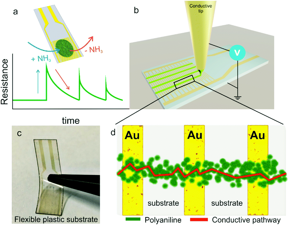 | ||
| Fig. 1 Gas sensing and sensor preparation schematic. (a) In the presence of ammonia, conductive polyaniline becomes more resistive. When exposure to ammonia ceases, the sensor recovers to its original baseline. It is possible to observe different peak heights depending on the concentration of ammonia exposed. (b) Electrohydrodynamic jet printing of polyaniline on the interdigitated electrodes. (c) An example of the flexible substrates used in this work. (d) Schematic of the movement of electrons through the discrete printed polyaniline. | ||
Experimental section
Preparation of polyaniline
Emeraldine base polyaniline (Mw avg = 50![[thin space (1/6-em)]](https://www.rsc.org/images/entities/char_2009.gif) 000) (Sigma Aldrich) was weighed out and dissolved in 20 mL of 1-methyl-2-pyrrolidone (NMP) (Sigma Aldrich). After complete dissolution, 5 mL aliquots of this stock solution were prepared in small glass vials. To convert the polyaniline from the insulating emeraldine base to the conducting emeraldine salt, 500 μL of acid (in excess) was added to each vial, with the following concentrations: (i) 250 mM HCl (Sigma Aldrich), (ii) 1:1 mixture of 250 mM camphorsulfonic acid (CSA) (Sigma Aldrich) and HCl, (iii) 250 mM CSA. The addition of HCl caused a mildly exothermic reaction. These newly doped solutions were ultra-sonicated for 15 minutes and then sealed before use. Caution: NMP is known to be a developmental toxicant. Extreme caution must be used, and exposure minimized.
000) (Sigma Aldrich) was weighed out and dissolved in 20 mL of 1-methyl-2-pyrrolidone (NMP) (Sigma Aldrich). After complete dissolution, 5 mL aliquots of this stock solution were prepared in small glass vials. To convert the polyaniline from the insulating emeraldine base to the conducting emeraldine salt, 500 μL of acid (in excess) was added to each vial, with the following concentrations: (i) 250 mM HCl (Sigma Aldrich), (ii) 1:1 mixture of 250 mM camphorsulfonic acid (CSA) (Sigma Aldrich) and HCl, (iii) 250 mM CSA. The addition of HCl caused a mildly exothermic reaction. These newly doped solutions were ultra-sonicated for 15 minutes and then sealed before use. Caution: NMP is known to be a developmental toxicant. Extreme caution must be used, and exposure minimized.
Polyaniline deposition
Dropcast films were prepared by casting 5 μL of polyaniline solution onto the interdigitated electrodes and allowing it to dry under ambient conditions. No heating was used, as acid would damage the electrodes at elevated temperatures.Printed lines are deposited using a custom-built EHD setup, described elsewhere.28 Briefly, gold coated conical glass capillaries (inner diameter 5–10 μm, World Precision Instruments) were filled with 50 μL doped polyaniline using microloader pipette tips. A voltage bias between the tip and the grounded substrate generates the electrostatic force to overcome the surface tension of the ink. Continuous printing was carried out when the Taylor cone formed (Fig. S2, ESI†). No other counter electrode was used to control printing direction. The substrate is moved in the X and Y direction using motorized stages which allows for directed printing of polyaniline. Applied voltages ranged from 2–10 kV (dependent on ink). The capillary-substrate stand-of height was 50–100 μm. This height is manually controlled using a calibrated piezo actuator (Video S1, ESI†).
Ammonia gas sensing
A custom-built gas chamber was used for all the sensing experiments. For each sensing measurement, the sample of interest was loaded and connected into the circuit. The chamber was then purged with 99.9% nitrogen gas for 30 minutes. After this purge, a baseline measurement in the presence of a constant nitrogen stream was taken for 1 hour to ensure sensor stability and a good reference. If the baseline was not stable in this time, the sample was removed and remade. For stable samples, exposition to ammonia occurred in 5 minute intervals, and then the nitrogen stream was restored to allow the sample to return to baseline readings. The current was monitored via the application of a potential bias (1 V) and recorded throughout this process on a computer interfaced with BenchVue software.Structural characterization
The morphology of the differently doped polyaniline was characterized and identified with different techniques. Firstly, optical images were taken of the IDEs before sensing to gain a sense of the distribution of the material (Nikon Eclipse LV100ND). Secondly, high resolution SEM images were obtained (Zeiss Merlin) for each sample to ascertain the structural information and arrangement on the IDEs. Further, a Malvern Mastersizer (Hydro 200 MU) and Nanosight LM10 were used to determine the size of the polyaniline particles in each dispersion. Lastly, powder XRD patterns (Bruker D500) were obtained to probe the crystallinity of each polyaniline sample.Results and discussion
Sensor devices
Three doping regimes were adopted in the preparation of the polyaniline used in this work. Hydrochloric acid (HCl), camphorsulfonic acid (CSA) and mixture of both these acids (co-doped) were used to make the polyaniline conductive (Fig. S1, ESI†). Both acids have been used before for polyaniline doping.10,16,29,30 IDEs on both glass (5 μm IDE spacing, Micrux) and plastic (100 μm IDE spacing, Dropsens) substrates were utilized in this study. The prepared sensors were tested in a custom-built gas chamber which was purged with nitrogen gas to remove any impurities.Dropcast-thin film sensors
Dropcast polymer films were first assessed for their sensing properties to compare with EHD printing. The dropcast film sensors were first assessed for electrical conductivity by using a voltmeter before being loaded into the gas chamber. Once loaded, they were purged under N2 for at least 30 minutes before a constant potential of 1 V was applied. After 1 hour of stabilization, ammonia was introduced into the chamber in controlled concentrations in 5 minute exposure periods. The differently doped films on glass substrates yielded incoherent sensing results. Whilst registering a slight increase in resistance, as is expected for a chemiresistor, the profiles observed were not as anticipated (Fig. 2). The HCl doped film (Fig. 2a), being the least resistive, demonstrated the clearest change of resistance with a 5 ppm ammonia exposure. After the ammonia exposure was stopped, the film showed no recovery to its baseline resistance. A subsequent 9 ppm exposure yielded no change. Both CSA and co-doped films, with higher resistances were less sensitive to changes in concentrations. A reasonable chemiresistor response to the exposure of an analyte gas would be a notable change in the resistance, and then recovery to the original baseline once the exposure is turned off.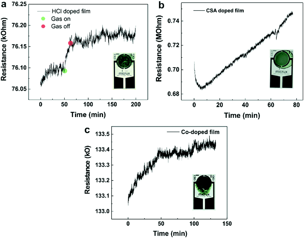 | ||
| Fig. 2 Sensing results of dropcast films on glass substrates. (a) HCl doped film shows no baseline recoverability after sensing. (b) CSA doped and (c) co-doped polyaniline have unstable baselines, thus are unsuitable for sensing applications. Even with prolonged exposure to ammonia, no change in the resistance observed. Inset images are photographs of each dropcast film. | ||
Exploring the thin film sensors on plastic substrates, we observed significantly different behavior. When ammonia was introduced, a rapid response was observed during the exposure period (5 minutes) (Fig. 3a, c and e). However, these sensors, too, were unstable. This is due to the lack of recovery after gas exposure was terminated. All three sensors did not recover to the original baseline even after at least 20 minutes of purging with nitrogen gas. We observed that for subsequent exposure periods with the same concentration of ammonia gas, the sensor response diminished each time, indicating possible saturation of the sensing layer (Fig. 3b, d and f). The deterioration of the response indicates that dropcast thin film sensors behave poorly and cannot be reliably used for quantification purposes.
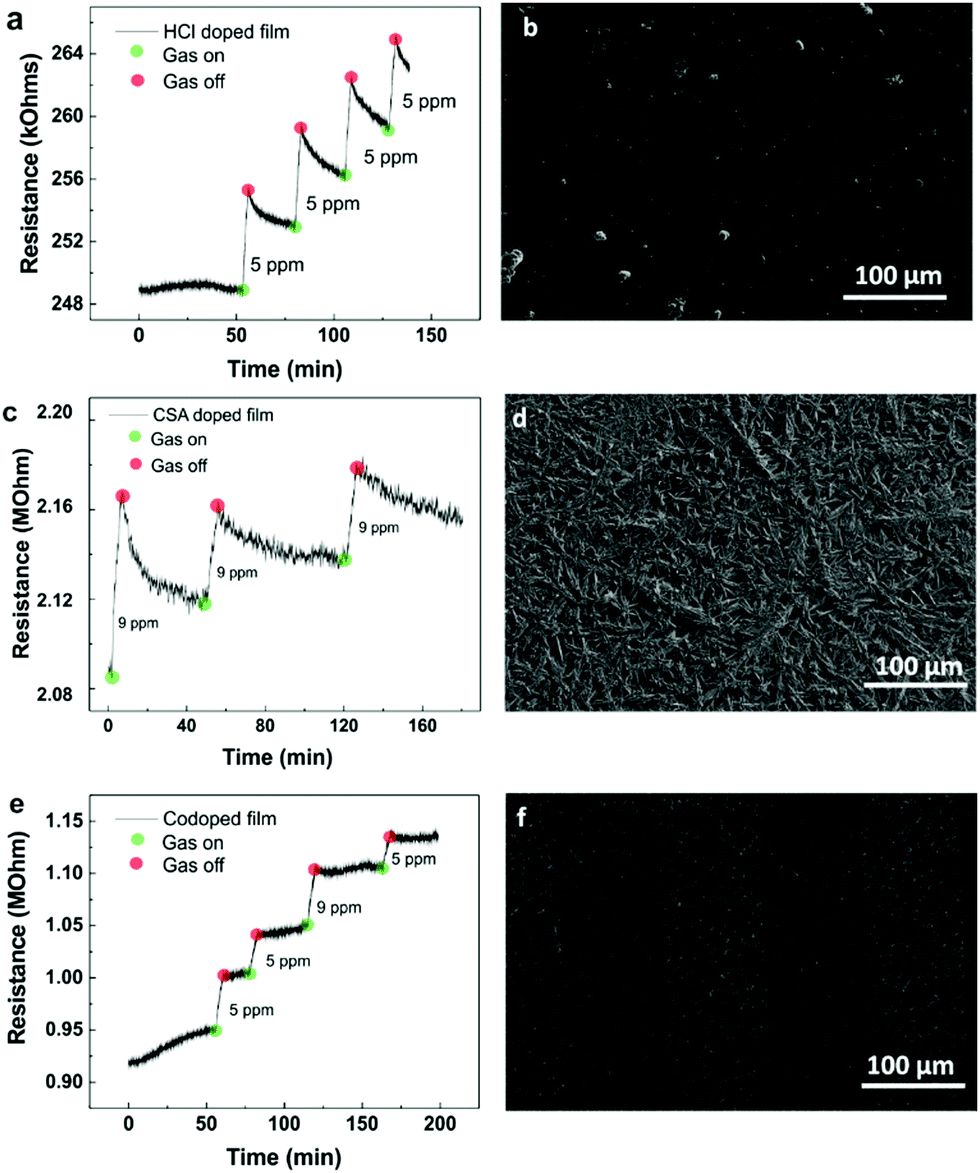 | ||
| Fig. 3 Dropcast sensor sensing results and SEM images on flexible plastic substrates. (a) HCl doped polyaniline. (c) CSA doped polyaniline. (e) Co-doped polyaniline. No recoverability was observed for any of the films. The corresponding SEM images (b, d and f) reveal the dense organization of the polyaniline on the electrodes. | ||
Sensor dependence on polyaniline morphology
The polyaniline films were prepared in the same manner on both glass and plastic substrates (see Methods section), however the sensing behavior observed on each substrate was different. Further, the response exhibited by each film varied depending on the dopant used, and SEM imaging revealed that each film was morphologically different (Fig. 4a–c). The HCl doped film appeared to be quite amorphous (or more powder-like) whereas the CSA doped film appeared more crystalline. The co-doped film was predominantly amorphous too, with some regions of higher crystallinity. To assess these trends further, XRD was employed to probe the structure (Fig. 4d). The measurements corroborated the observations made from the SEM images, with the HCl doped film having the least crystallinity. CSA films registered the highest crystallinity as confirmed by the numerous diffraction peaks. The SEM images also reveal very dense packing of the polyaniline on the substrates. We hypothesize that this may be a strong cause for the poor sensing observed. If only the surface of the polyaniline sensing layer is exposed to the ammonia, then very little electrical change will be detected, as the bulk of the material will still be conductive. This would be due to poor diffusion of gas to reaction sites.31 We found that the polyaniline on the plastic substrates spread out more than on the glass substrate, thus resulting in thinner films. This increased surface area allows for better ammonia diffusion.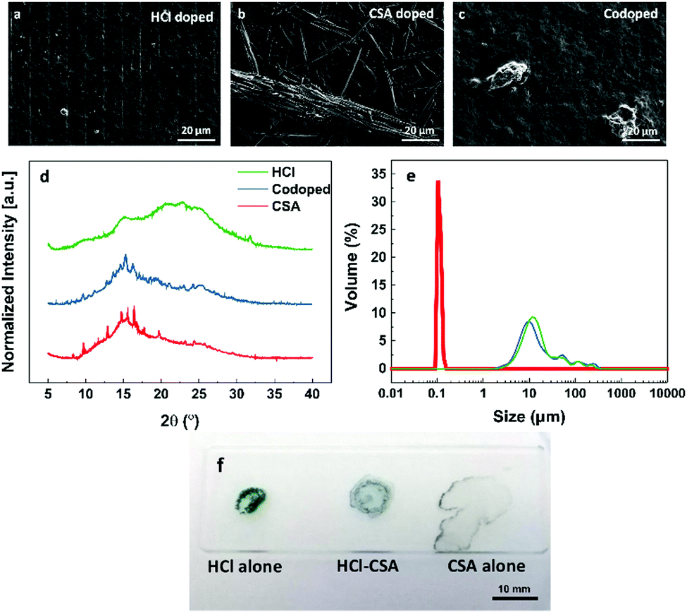 | ||
| Fig. 4 Characterization of polyaniline blends. SEM images of (a) HCl doped, (b) CSA doped and (c) co-doped polyaniline material. (d) Powder XRD spectra of differently doped polyaniline samples. The presence of CSA causes an increase in the crystallinity, as evidenced by the sharp crystalline peaks. (e) Particle size distribution for differently doped polyaniline mixtures used in this study. CSA doped polyaniline (red) has an average particle size of 130 nm, whereas HCl doped (green) and co-doped (blue) mixtures have an average size of almost 10 μm. (f) Spreading and drying behavior of polyaniline suspensions on a glass substrate. A 10 μL drop of each suspension was deposited on a glass slide and allowed to evaporate in ambient conditions. The surface to volume ratio of each drop is 3, 7, and 18 mm−1 respectively, quantifying the degree of wetting each drop achieves. | ||
Thus, we propose that for highly sensitive sensing to occur, discrete regions of polyaniline must be deposited, in order to maximize the polymer interaction volume, and therefore the change in resistance observed. Electrohydrodynamic jet printing (EHD) was employed to achieve this. EHD makes use of an electric field to release a conductive ink from a fine capillary (Fig. S2, ESI†). High printing resolution can be obtained using EHD as the geometry of the jet is not limited by the nozzle size, but rather by the applied potential. Therefore, discrete patterns can be obtained during this printing. A condition for good quality printing to occur is that the ink itself be processable, and not liable to clog the nozzle. Clogging is a common occurrence where nozzles with small dimensions are used (more especially for inkjet printing). Notably, work has been done with nozzle-less printheads, using other forms of actuation such as pyro-electrodynamic shooting which serve to overcome this limitation in EHD printing.32–35 In this work, doped polyaniline exists as a suspension in the solvent. Thus, particle size analysis was performed to quantify the size of the polyaniline particles (Fig. 4e). We observed that the HCl doped and co-doped polyaniline had a similar particle size distribution of an average of 10 μm due to their insolubility. The CSA doped polyaniline had a particle size distribution averaging 100 nm, owing to the higher solubility of this moiety.16 The particle size also has a strong influence on the rheology of the polyaniline inks. Fig. 4f demonstrates how the three polyaniline inks wet a glass slide. Single 10 μL droplets were cast on the glass and allowed to spread and dry. The HCl doped droplet does not spread notably, similarly with the co-doped droplet. The CSA doped droplet, however, spreads significantly, resulting in large inter-particle distances. This difference in wetting has significant ramifications, the most notable of which is the conductivity of each ink. The HCl doped ink is more conductive than the co-doped ink, which in turn is more conductive than the CSA doped ink. The surface to volume ratio of the HCl, co-doped and CSA drops are 3, 7 and 18 mm−1 respectively, further quantifying how much each droplet spreads on the surface.
EHD printed sensors
The polyaniline blends were printed in turn using a gold-coated glass capillary with 5 μm nozzle. A working voltage of between 2 and 10 kV was used. The HCl doped polyaniline, with 10 μm particle size distribution exhibited poor printing due to nozzle clogging (Fig. S3, ESI†). As the clogging was due to aggregation of the polyaniline, surfactant was introduced to try encourage the solubility. However, UV-Vis spectroscopy revealed that this had no impact on the spectral properties, and therefore the size of the aggregated particles (Fig. S4 and Table S1, ESI†). The SEM image of the IDE reveals the poor level of polyaniline connectivity. Due to this poor printing, the sensor was not able to function. Better printing was observed however for both the CSA doped and co-doped polyaniline blends (Fig. 5a and d). Both sensors displayed typical chemiresistive behavior when the ammonia concentration was varied from 5 ppm down to 0.2 ppm during 5 minute exposure windows. Subsequent concentrations were introduced once the sensor had recovered to its original baseline. Previously reported EHD printed CSA doped polyaniline responded to a minimum concentration of 300 ppm.36 The peak resistance reached during each exposure was then used to determine the calibration plot for the sensor (Fig. 5b and e). From this, the limit of detection (LOD), based on three times the standard deviation of the line of best fit from the calibration graph, was calculated (Table S2, ESI†). For the CSA doped sensor, the LOD was calculated to be 0.22 ppm (sensitivity = 2.5% ppm−1), and the LOD of the co-doped sensor was found to be 0.86 ppm (sensitivity = 0.5% ppm−1). The discrepancy between the 0.2 ppm exposure and the co-doped LOD of 0.86 ppm is due to physical nature of the co-doped polyaniline. As observed with the thin film sensors, co-doped polyaniline is still deposited in a thicker film arrangement compared to the crystalline CSA doped polyaniline. This makes the recovery of the baseline more challenging, especially for lower concentrations, leading to a slight nonlinearity of the calibration plot. This then translated to a suboptimal approximation of the LOD. When the printing was attempted on the flexible substrates, only the HCl doped polyaniline was successfully deposited (Fig. 6a). This is for several reasons. Firstly, EHD printing is most successful on conductive substrates. The IDE spacing on the flexible substrates was 100 μm, meaning that the field strength varied quite significantly during printing, compared to the more constant field over the 5 μm spaced IDEs on glass. Secondly, the HCl doped polyaniline blend is the most conductive (as per voltmeter measurements). If no clogging occurs, this blend is the most likely to print on large nonconductive areas which makes their use in commercially available IDES on flexible substrates very attractive as it is challenging to obtain IDEs on flexible substrates with smaller finger gaps than 100 μm due to the limiting nature of the resolution of photolithography techniques used in their manufacturing. However, in saying that, by exploiting the synergy between the HCl doped polyaniline material and the nature of the flexible substrate it opens up a unique way of mass printing sensing layers on flexible substrates. It is also interesting to note the arrangement of the polyaniline on the flexible IDE. The bulk of the material bridges the electrodes, with small amounts on the metal fingers themselves (Fig. 6c). Another interesting point to note in Fig. 6 is the bright charging effect that is visible between the gaps of the polymer print fronts. This charging effect is present due to the combination of the insulating nature of the flexible substrates together with the large gap size of 100 μm. This charging effect, which is usually seen as a negative outcome for imaging, can be used here to our advantage to view the polymer bridges.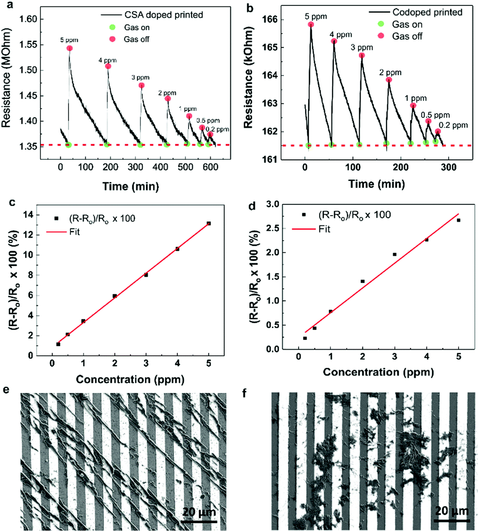 | ||
| Fig. 5 Sensing and calibration graphs for printed sensors on glass substrate. (a) CSA doped polyaniline sensing (baseline = 1.36 MΩ) and the corresponding (c) calibration graph. (e) SEM image of printed CSA doped polyaniline reveals the increased level of bridging between electrodes. (b) Co-doped polyaniline sensing (baseline = 161.6 kΩ) and (d) calibration graph. (f) SEM shows the quality of printing, and provides visual evidence of bridging. | ||
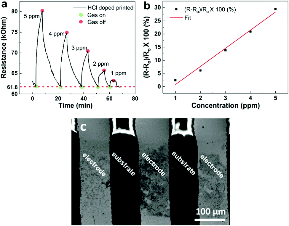 | ||
| Fig. 6 Sensing and calibration graphs for HCl doped polyaniline on flexible substrate. (a) Significant changes in the resistance were registered between 1 and 5 ppm for this sensor (baseline = 61.8 kΩ). (b) The calibration curve gives an approximate limit of detection of 0.74 ppm. (c) SEM image of the printed line reveals the spreading of the polyaniline ink more over the plastic substrate compared to the gold electrode. | ||
The LOD calculated for the flexible substrate sensor was 0.74 ppm (sensitivity = 6.9% ppm−1) which was highly encouraging and shows the possibility of using EHD printing as a tool to prepare flexible sensors. Fig. S5 (ESI†) illustrates how the polyaniline bridging is better on glass substrate than on the flexible substrates for the CSA doped and co-doped blends and vice versa for the HCl blends. This is largely due to the distance between the electrodes, 5 μm for the glass and 100 μm for the plastic substrates. Finally, Fig. S6 (ESI†) consolidates the importance of EHD printing. EHD offers focused deposition of the polymer sensing material onto the desired regions. The use of another deposition method, such as spin-coating, results in poorly formed films, which contribute to poor or no sensing whatsoever.
Conclusion
Here we have shown that using discrete printed arrays of polyaniline can result in higher sensitivity and better performing sensing, with the sensing of 200 ppb of ammonia gas using CSA doped and co-doped polyaniline. The EHD printing method employed allows for the printing on both flexible and rigid substrates and can be used to create miniature devices and for mass printing. Our results corroborate the known influence of dopant acid on the overall polyaniline conductivity and morphology and illustrates for the first time how these factors influence sensing and printability. We found that camphorsulfonic acid doped polyaniline was the best for use with EHD printing of the blends tested due to the superior solubility and processability on glass substrates. Any clogging of the ink can lead to poor printing and thus sensing, therefore ink rheology an important consideration. The polyaniline morphology is crucial to the resistivity observed, as well as the recoverability of the sensor. We have also shown that the HCl doped polyaniline sensor can be prepared on flexible substrates. This work paves the way for the development of new flexible sensors which can easily be integrated into wearables or electronic devices. This will create new opportunities for the implementation of miniaturized flexible sensors in areas such as environmental monitoring, and diagnostics in healthcare.Author contributions
The manuscript was written through contributions of all authors. All authors have given approval to the final version of the manuscript.Conflicts of interest
There are no conflicts to declare.Acknowledgements
The authors acknowledge support from EPSRC via the Manufacturing Fellowship EP/J018694/1 as well as the WAFT collaboration (EP/M015173/1). N. M. acknowledges the Rhodes Trust, the Oppenheimer Memorial Trust, and the Wadham College Senior Scholarship for financial support. Thank you to the Oxford Material Characterization Service for access to XRD and particle size analysis equipment.References
- M. Van Damme, L. Clarisse, S. Whitburn, J. Hadji-Lazaro, D. Hurtmans, C. Clerbaux and P. Coheur, Nature, 2018, 564, 99–111 CrossRef CAS PubMed
.
- Y. Seekaew, S. Lokavee, D. Phokharatkul, A. Wisitsoraat, T. Kerdcharoen and C. Wongchoosuk, Org. Electron. Phys., Mater. Appl., 2014, 15, 2971–2981 CAS
- A. Dey, Mater. Sci. Eng., B, 2018, 229, 206–217 CrossRef CAS
- H. Wu, Z. Ma, Z. Lin, H. Song, S. Yan and Y. Shi, Nanomaterials, 2019, 9, 388 CrossRef CAS PubMed
- G. F. Fine, L. M. Cavanagh, A. Afonja and R. Binions, Sensors, 2010, 10, 5469–5502 CrossRef CAS PubMed
- Z. Li, H. Li, Z. Wu, M. Wang, J. Luo, H. Torun, P. Hu, C. Yang, M. Grundmann, X. Liu and Y. Fu, Mater. Horiz., 2019, 6, 470–506 RSC
- E. Comini, Sensors, 2013, 13, 10659–10673 CrossRef CAS PubMed
- D. Yang, I. Cho, D. Kim, M. A. Lim, Z. Li, J. G. Ok, M. Lee and I. Park, ACS Appl. Mater. Interfaces, 2019, 11, 24298–24307 CrossRef CAS PubMed
- X. Q. Zheng and H. Y. Cheng, Sci. China: Technol. Sci., 2019, 62, 209–223 CrossRef CAS
- I. Fratoddi, I. Venditti, C. Cametti and M. V. Russo, Sens. Actuators, B, 2015, 220, 534–548 CrossRef CAS
- H. Bai and G. Shi, Sensors, 2007, 7, 267–307 CrossRef CAS
- S. Li, Y. Li, S. Chen, W. Tang, Y. Huang, S. Peng, J. Qi and X Guo, IEEE Sensors Letters, 2018, 2, 1–4 Search PubMed
- J. Cai, C. Zhang, A. Khan, C. Liang and W. D. Li, RSC Adv, 2018, 8, 5312–5320 RSC
- R. M. Morais, M. D. S. Klem, G. L. Nogueira, T. C. Gomes and N. Alves, IEEE Sens. J., 2018, 18, 2647–2651 CAS
- K. Crowley, A. Morrin, A. Hernandez, E. O. Malley, P. G. Whitten, G. G. Wallace, M. R. Smyth and A. J. Killard, Talanta, 2008, 77, 710–717 CrossRef CAS
- D. Nicolas-Debarnot and F. Poncin-Epaillard, Anal. Chim. Acta, 2003, 475, 1–15 CrossRef CAS
- N. J. Pinto, I. Ramos, R. Rojas, P. Wang and A. T. Johnson, Sens. Actuators, B, 2008, 129, 621–627 CrossRef CAS
- S. Manigandan, S. Majumder, S. Ganguly and K. Kargupta, Mater. Lett., 2008, 62, 2758–2761 CrossRef CAS
- D. K. Bandgar, S. T. Navale, S. R. Nalage, R. S. Mane, F. J. Stadler, D. K. Aswal, S. K. Gupta and V. B. Patil, J. Mater. Chem. C, 2015, 3, 9461–9468 RSC
- P. P. Sengupta, S. Barik and B. Adhikari, Mater. Manuf. Processes, 2006, 21, 263–270 CrossRef CAS
- K. Murugappan and M. R. Castell, Electrochem. Commun., 2018, 87, 40–43 CrossRef CAS
- B. I. Armitage, K. Murugappan, M. J. Lefferts, A. Cowsik and M. R. Castell, J. Mater. Chem. C, 2020, 8, 12669–12676 RSC
- N. R. Tanguy, M. Thompson and N. Yan, Sens. Actuators, B, 2018, 257, 1044–1064 CrossRef CAS
- J.-U. Park, M. Hardy, S. J. Kang, K. Barton, K. Adair, D. K. Mukhopadhyay, C. Y. Lee, M. S. Strano, A. G. Alleyne, J. G. Georgiadis, P. M. Ferreira and J. A. Rogers, Nat. Mater., 2007, 6, 782–789 CrossRef CAS PubMed
- A. Jaworek and A. Krupa, J. Aerosol Sci., 1999, 30, 873–893 CrossRef CAS
- S. N. Jayasinghe and M. J. Edirisinghe, Appl. Phys. Lett., 2004, 85, 4243–4245 CrossRef CAS
- M. W. Lee, D. K. Kang, N. Y. Kim, H. Y. Kim, S. C. James and S. S. Yoon, J. Aerosol Sci., 2012, 46, 1–6 CrossRef CAS
- B. F. Porter, N. Mkhize and H. Bhaskaran, Microsyst. Nanoeng., 2017, 3, 17054 CrossRef CAS PubMed
- Y. Xia, J. M. Wiesinger, A. G. MacDiarmid and A. J. Epstein, Chem. Mater., 1995, 7, 443–445 CrossRef CAS
- W. ŁUzny and E. Bańka, Macromolecules, 2000, 33, 425–429 CrossRef
- H. Kebiche, D. Debarnot, A. Merzouki, F. Poncin-Epaillard and N. Haddaoui, Anal. Chim. Acta, 2012, 737, 64–71 CrossRef CAS PubMed
- L. Mecozzi, O. Gennari, S. Coppola, F. Olivieri, R. Rega, B. Mandracchia, V. Vespini, A. Bramanti, P. Ferraro and S. Grilli, ACS Appl. Mater. Interfaces, 2018, 10, 2122–2129 CrossRef CAS PubMed
- S. Coppola, G. Nasti, M. Todino, F. Olivieri, V. Vespini and P. Ferraro, ACS Appl. Mater. Interfaces, 2017, 9, 16488–16494 CrossRef CAS PubMed
- S. Coppola, V. Vespini, G. Nasti, O. Gennari, S. Grilli, M. Ventre, M. Iannone, P. A. Netti and P. Ferraro, Chem. Mater., 2014, 26, 3357–3360 CrossRef CAS
- L. Mecozzi, O. Gennari, R. Rega, S. Grilli, S. Bhowmick, M. A. Gioffrè, G. Coppola and P. Ferraro, Soft Matter, 2016, 12, 5542–5550 RSC
- Z. Zhan, G. Zheng, W. Tao, Y. Cai, D. Sun and D. Wu, J. Nanoeng. Nanosyst., 2012, 226, 9–13 CAS
Footnotes |
| † Electronic supplementary information (ESI) available: Schematic of reaction between ammonia and polyaniline, schematic and mechanism of EHD operation, effect of nozzle clogging on sensing, UV/Vis characterization of polyaniline, further SEM images of polyaniline bridging on substrates, limit of detection data, microscope image of spin-coated polyaniline on silica surface. (docx) Video of EHD printing of polyaniline onto flexible plastic substrate. (Video, MP4). See DOI: 10.1039/d0tc05719c |
| ‡ These authors contributed equally. |
| This journal is © The Royal Society of Chemistry 2021 |