
 Open Access Article
 This Open Access Article is licensed under a Creative Commons Attribution-Non Commercial 3.0 Unported Licence
Elucidating the growth mechanism of ZnO films by atomic layer deposition with oxygen gas via isotopic tracking†
Tai
Nguyen
 ab,
Nathalie
Valle
a,
Jérôme
Guillot
a,
Jérôme
Bour
a,
Noureddine
Adjeroud
a,
Yves
Fleming
a,
Mael
Guennou
b,
Jean-Nicolas
Audinot
a,
Brahime
El Adib
a,
Raoul
Joly
ab,
Didier
Arl
a,
Gilles
Frache
a and
Jérôme
Polesel-Maris
*a
ab,
Nathalie
Valle
a,
Jérôme
Guillot
a,
Jérôme
Bour
a,
Noureddine
Adjeroud
a,
Yves
Fleming
a,
Mael
Guennou
b,
Jean-Nicolas
Audinot
a,
Brahime
El Adib
a,
Raoul
Joly
ab,
Didier
Arl
a,
Gilles
Frache
a and
Jérôme
Polesel-Maris
*a
aMaterials Research and Technology Department, Luxembourg Institute of Science and Technology, 41, rue du Brill, L-4422 Belvaux, Luxembourg. E-mail: jerome.polesel@list.lu
bDepartment of Physics and Materials Science, University of Luxembourg, 41 rue du Brill, L-4422 Belvaux, Luxembourg
First published on 15th March 2021
Abstract
The growth process of zinc oxide (ZnO) thin films by atomic layer deposition (ALD) accompanied by the presence of oxygen gas pulsing is investigated by means of the isotopic tracking of oxygen 18O from the water precursor and oxygen 16O from the gas. In a previous study [T. Nguyen et al., Results Mater., 2020, 6, 100088, DOI: 10.1016/j.rinma.2020.100088], by means of structural, electrical, and optical characterizations, we identified key growth parameters of this unusual ALD process. Unexpectedly, the influence of molecular oxygen on the crystallography, microstructure, and morphology of the hundred-nanometer- to micrometer-thick ZnO films was significant. In this study, we present an unprecedented methodology by combining isotopic tracers with mass spectrometry to elucidate the role of the two different sources of oxygen atoms during the evolution of the growth. Notably, the use of in situ quartz crystal microbalance (QCM) and Secondary Ion Mass Spectrometry (SIMS) reveals new insights into the reaction mechanism for ZnO thin film growth. On the one hand, the non-negative mass change during the ZnO growth without O2 gas is attributed to the presence of bare zinc atoms on the surface due to the reaction between monoethyl zinc and hydroxyl groups of the water precursor after the diethyl zinc pulse. On the other hand, the detection of ZnxOyC2H5− ions by Time-of-Flight SIMS (TOF-SIMS) and the mass increase during the O2 pulse suggest a new reaction mechanism for the ZnO thin film growth in the presence of gaseous O2 where the ethyl ligand of the zinc precursor can react with O2 to form ethylperoxy radicals. The formations of the ethylperoxy zinc and/or zinc atoms lead to more adsorption of water to form ethylhydroperoxide during the water pulse, inducing the positive mass change. The use of an isotopic substitution allowed us to unambiguously associate the mass gain with the gradual incorporation of gaseous oxygen throughout the growth process and thereby support the chemical reaction.
1. Introduction
A proper control over the crystallographic structure of ZnO thin films and their properties is needed for various applications, such as optoelectronics,1 solar-based devices,2 harvesters, sensors and actuators.3–7 This control is usually achieved by varying the single crystal substrates8–11 and the deposition temperature,12–15 however practical applications are limited due to requirements in the crystallographic structure of substrates, as well as elevated deposition temperatures. Park et al.,16 and our previous study17 demonstrated that the crystallographic structure, the optical and the electronic properties of ZnO thin film were highly tuned by the introduction of gas pulsing of molecular oxygen during atomic layer deposition growth at quite low temperatures (100–200 °C) and even on glass substrates. The randomly oriented film structure was transformed into a highly preferred (002) orientation. Concomitantly, the ZnO thin films obtained were electrically more resistive (by 3 to 4 orders of magnitude) with a wider bandgap and a substantially weaker deep-level emission (DLE) in photoluminescence spectra, i.e. green, yellow-orange, and red emissions. However, there are still questions about the adsorption of oxygen inside the ZnO film or its desorption after each ALD cycle. In addition, the deposition of ZnO from diethylzinc (DEZ) and water precursors follows the net reaction:| Zn(C2H5)2 + H2O → ZnO + 2C2H6 | (R1) |
| DEZ pulse: Zn(C2H5)2 + I–OH →I–O–Zn–C2H5 + C2H6 | (R2a) |
| Water pulse: H2O + I–O–Zn–C2H5 → I–O–Zn–OH + C2H6 | (R3) |
| I–O–Zn–C2H5 + I–OH → (I–O)2–Zn + C2H6 | (R2b) |
Here, we address these issues using an innovative approach based on a combination of isotopic substitution during the film growth and secondary ion mass spectrometry (SIMS) to monitor the contribution of each source of oxygen atoms. We used 18O-labelled water as a precursor in order to distinguish between the respective contributions of oxygen atoms from water precursor (H218O) and from gaseous oxygen (16O2). In situ quartz crystal microbalance (QCM) was implemented to study the effect of oxygen presence on the ALD growth characteristics of ZnO thin films. In addition, time-of-flight SIMS (ToF-SIMS) was carried out to identify the resulting chemical composition of the ZnO thin films.
2. Experimental procedure
ZnO thin films were grown with a commercial ALD reactor (Beneq, TFS 200) in thermal configuration. Details of the ALD growth can be found in our previous report.17 In the present work, 18O-labeled deionized (DI) water (Sigma-Aldrich, Ref. ALDRICH: 329878, isotopic purity of 97 at% 18O) was used. The oxygen gas was delivered by a stand-alone bottle (Air Liquide, alpha 2 O2 global purity ≥99.9995% mol with less than 0.5 H2O ppm mol impurity) in the ALD reactor. The argon gas used for purging during the ALD process was ALPHAGAZ™ 2 with a global purity of ≥99.9999% mol with less than 0.5 H2O ppm mol impurity. The supporting surfaces for the ZnO thin film deposition were 2 × 2 cm2 pieces of pristine single crystal Si(100) wafer (Siegert GmbH, Germany, grade Monitor) and glass slides (Thermo Scientific, Germany). Prior to the synthesis of ZnO thin films, the substrates were cleaned in acetone, isopropanol, conventional DI water and finally dehydrated on a hotplate for 20 minutes at 200 °C. Just before their introduction into the ALD reactor, an additional plasma cleaning (Plasma Therm 790 RIE, 120 W, 10 minutes, in Ar:O2 gas environment at 30 mTorr) was performed on the substrates. ZnO thin films without oxygen gas were synthesized at a deposition temperature of 180 °C by the following sequence of four steps: diethylzinc (DEZ) pulse (0.1 s), Ar purge (5 s), H218O pulse (0.1 s), and Ar purge (5 s). The ZnO thin films with the presence of oxygen gas were deposited at 180 °C by a sequence of six pulses; DEZ pulse (0.1 s), Ar purge (5 s), O2 pulse (1 s), Ar purge (20 s), H218O pulse (0.1 s), and Ar purge (10 s). Both films were grown with 500 cycles corresponding to thicknesses of 96 and 120 nm for ZnO thin films synthesized with and without gaseous oxygen, respectively. In situ QCM (Q-Pod Quartz Monitor, IPN 074-547-P1B, INFICON Inc.) was implemented in the ALD reactor to track mass variations during the growth. The mass change is detected by measuring the change of the resonance frequency of the quartz sensor, as given by the equation below:20| Δm/S = −(μρ)0.5Δf/(2f02) | (1) |
X-ray diffractometry (Diffractometer Bruker D8 Discover with Cu Kα radiation and a 5-axis Eulerian cradle) was conducted in θ–2θ configuration to examine the crystalline quality of the ZnO thin films on all samples. The microstructure of samples was studied by scanning electron microscopy (SEM) on a Helios Nanolab 650 FIB-SEM instrument (FEI Company, USA). A four-point probe (Ecopia HMS-3000) was performed to measure the resistivity of the thin film on glass substrates. Elemental composition and chemical states were investigated by X-ray photoelectron spectroscopy (XPS) (Axis Ultra DLD, Kratos Analytical Ltd) over a surface area of 110 × 110 μm2 using an X-ray source (Al Kα monochromated, E = 1486.6 eV) at a power of 150 W, and an energy resolution of 1.5 eV for survey scans and 0.55 eV for narrow scans determined on a silver sample. The spectra were calibrated in energy from the Zn 2p peak in ZnO at 1022.0 eV. The surface contamination was removed by etching an area of 3 × 3 mm2 with an Ar+ ion beam operating at 2 kV and 2 μA.
The transmittance and reflection spectra of ZnO thin films on glass slides were collected by UV-visible measurements (LAMBDA 1050 UV/Vis Spectrometer, PerkinElmer) in a 250–2000 nm range. Room-temperature photoluminescence (PL) spectra were acquired by a Renishaw inVia confocal microRaman spectrometer using an excitation wavelength of 325 nm produced by an 8 mW He–Cd laser focused through a Thorlabs UV objective with 40× magnification and a numerical aperture of 0.5. A 300 g mm−1 grating enabled analysis in the 350–900 nm range. A single crystal ZnO (MTI Corporation) was used as a reference.
Dynamic-secondary ion mass spectrometry (D-SIMS) (CAMECA SC-Ultra) was used to analyze the elemental and isotopic composition of the films grown. First, depth profiles were acquired with a Cs+ bombardment operating at 1 keV and a 6 nA primary ion beam scanned over an area of 500 × 500 μm2. Secondary positive ions were detected as MCs+ clusters (M is the element of interest) from a 60 μm area centered on the scanned area. Secondly, the oxygen isotopic signatures were determined with the M− mode analysis over an area with a diameter of 8 μm. A mass resolution of 1000 allowed isobaric interference on 18O to be eliminated.
A Helium Ion Microscope (HIM, Nanofab, ZEISS, Peabody, USA) coupled with in-house SIMS system (HIM–SIMS)21,22 was used to analyze and map the 16O and 18O isotopes. SIMS images were acquired by collecting the secondary ions emitted from the film surface scanned by a 20 keV Ne+ ion beam of 2 pA over a matrix of 512 × 512 pixels with a counting time of 5 ms per pixel.
The time-of-flight secondary ion mass spectrometry experiments were performed using a commercial TOF-SIMS V time-of-flight mass spectrometer (ION-TOF GmbH, Münster, Germany) operating at a pressure of 10−9 mbar. Mass spectra were carried out with a 25 keV pulsed Bi3+ cluster ion source, delivering a 0.31 pA target current. The analyzed area was 500 mm × 500 mm. The analyses were performed using a primary ion dose density maintained at 1011 ions per cm2, which is below the so-called static SIMS limit. In these conditions, secondary ions are produced, reflecting the molecular and elemental composition of the first nanometer of a sample. The data were obtained in negative mode and the secondary ion mass spectra were calibrated using Cn– carbon clusters.
3. Results
3.1. Microstructural, optical, and electronic properties
Fig. 1 shows the XRD results and SEM images of the ZnO thin films grown with and without a 1 s pulsing of oxygen gas by ALD loop at a sample temperature of 180 °C. The diffraction patterns match the standard diffraction patterns of the hexagonal wurtzite ZnO crystal structure (JCPDS-36-1451). The film grown without the presence of oxygen gas at the same deposition temperature shows a polycrystalline structure consisting of a random distribution of (100), (002), and (101) orientations (Fig. 1(a)). The top-view SEM micrograph further confirms that different grain shapes co-exist, with wedge-shaped crystallites parallel to the substrate surface and fine-columnar crystallites perpendicular to the substrate surface. The ZnO film grown in the presence of oxygen gas, however, shows a preferred (002) orientation (Fig. 1(b)), which is further supported by a top-view SEM image of the film where fine-columnar crystallites are mainly identified.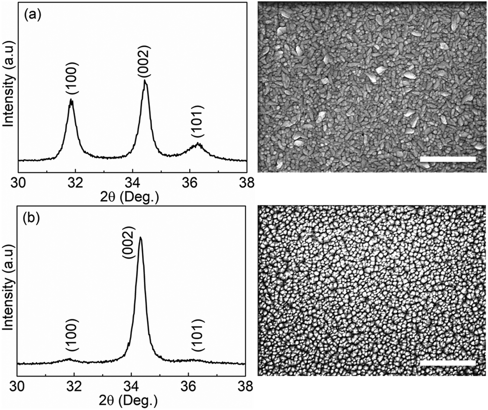 | ||
| Fig. 1 XRD patterns and top-view SEM images of (a) the ZnO thin film grown without, (b) with gaseous oxygen. The scale bar in the SEM images is 300 nm. | ||
The optical bandgap of ZnO thin films is derived from the Tauc plot, as shown in Fig. 2(a). The reflectance and transmittance spectra of ZnO thin films and a glass slide were carried out to calculate the absorption spectra of ZnO thin films. For a direct bandgap semiconductor,23 the relationship between the absorption coefficient α and photon energy hν is given by: (αhν)2 = A(hν − Eg), where h is Planck's constant, A is a constant and Eg is the optical bandgap. The bandgap is determined by extrapolating the linear part of the Tauc plots to α = 0, which is 3.2 eV for ZnO thin films grown without oxygen gas and increases up to 3.3 eV for the film grown with the 1 s pulse of oxygen.
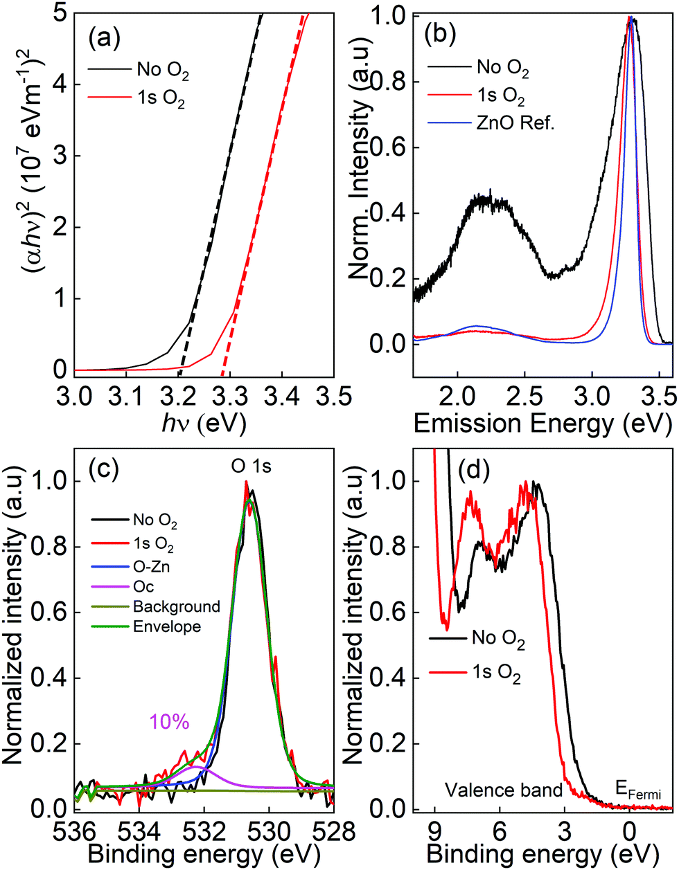 | ||
| Fig. 2 (a) Tauc plots of ZnO thin films grown with and without gaseous oxygen, (b) photoluminescence spectra of the ZnO thin films and a reference ZnO single crystal, (c) XPS narrow scans of O 1s spectra, (d) the valence band spectra of the ZnO thin films. The peak fitting on (c) was performed on the O 1s peak of the ZnO thin film grown in the presence of gaseous oxygen. The O 1s peak was deconvoluted into two peaks: a main peak O–Zn (530.6 eV) and a secondary peak Oc (532.2 eV) for hydroxides and/or chemisorbed oxygen. | ||
Fig. 2(b) presents the normalized photoluminescence spectra performed at room temperature. The strong energy peak located from 3.28 to 3.31 eV is assigned to the near band edge (NBE) emission. A broad emission band (1.5 to 2.7 eV) is observed that results from defect-related DLE and can be deconvoluted into green (2.58 to 2.25 eV), yellow-orange (2.25 to 2.03 eV), and red (2.03 to 1.64 eV) emission bands. Although the nature of the deep-level emission is controversial, there are three main arguments that are widely accepted:24,25
(i) The green emission is associated either with oxygen vacancies simply ionized  , oxygen antisites, or even zinc vacancies
  .
.
(ii) The yellow-orange emission corresponds to oxygen vacancies doubly ionized (VO°°).
(iii) The red emission is attributed to excess oxygen on the ZnO surface.
Interestingly, by adding oxygen molecules during the ALD process, the DLE region became minor compared to the NBE emission peak, whereas the DLE region can be clearly observed for ZnO thin film processed without oxygen gas at the same deposition temperature.
The chemical state and environment of oxygen and zinc were studied by X-ray photoelectron spectroscopy, as shown in Fig. 2(c) and (d). The Zn 2p peak is not affected by the presence of oxygen gas (not shown). In contrast, an additional peak located above 530 eV is observed in the O 1s spectrum when oxygen gas is added during the ALD processes (Fig. 2(c)). In general, the O 1s peak in ZnO compounds can be split into two components: a main peak related to the O–Zn bonds in the hexagonal wurtzite ZnO structure (∼530.60 eV),26–28 and an additional peak located at ∼532.2 eV assigned to hydroxides29,30 or to chemisorbed oxygen.27,28 The O 1s spectra acquisition was completed in less than 300 s after the end of the Ar sputtering to limit the adsorption of hydroxides occurring even under ultra-high vacuum on Zn dangling bonds present at the surface of the film (Fig. 2(c)). It can clearly be seen that not only O but also hydroxides are inserted inside the bulk of the film during the ZnO growth only when oxygen gas is added. This is also confirmed by the higher hydrogen level found in the SIMS depth profiles (Fig. 5(a) and (b)). They represent around 10% of the oxygen in the ZnO network. The valence band shape, sensitive to the filling of the oxygen vacancies, is also modified when adding oxygen gas into the synthesis process (Fig. 2(d)). The two structures around 4 eV and 7.5 eV are mainly due to electrons in the O 2p orbitals and the O 2p–Zn 4sp hybridized state respectively.31–33 An increase of the O 2p–Zn 4sp states, meaning these orbitals are more populated, is observed when oxygen gas is added during the synthesis process and is linked to a higher number of zinc atoms surrounded by oxygen atoms (O and/or OH) in the final wurtzite structure, thus decreasing the vacancy density in the film. Furthermore, the valence band positions of the two samples (determined without any energy calibration) clearly show a shift of 0.5 eV. Without the O2 pulse in the synthesis process, the Fermi level is closer to the conduction band, due to the higher oxygen vacancies amount in this n-type material. Based on this result, it is worth noting that the defects density due to oxygen vacancies (sample without O2 pulse) is much higher than the defects related to the incorporation of carbon resulting of the incomplete decomposition of DEZ (sample with the O2 pulse). This is confirmed by the fact that a peak shape evolution is observed in the O 1s spectrum versus the synthesis condition whereas carbon has not been detected in any sample by XPS whose sensitivity is lower than dynamic or ToF-SIMS. The O/Zn ratio was found to be 0.96 ± 0.03 and 0.92 ± 0.02 for the ZnO films grown with and without O2.
3.2. The in situ QCM characteristics of the ALD ZnO thin films
Fig. 3 presents the in situ QCM characteristics of the ZnO thin film grown without using oxygen gas pulsing. The timing sequence can be written as 0.1 s (DEZ pulsing)–5 s (Ar purging)–0.1 s (18O-labeled DI water pulsing)–5 s (Ar purging). The whole growth processes present a linear dependence of the mass gain with deposition time, as shown in Fig. 3(a). Noticeable features visible in the QCM curve are the presence of regular steps, which are clearly observed in the enlarged views of the QCM curves for selected periods, as presented in Fig. 3(b)–(d). As can be seen in the first stages of the growth before 500 seconds corresponding to about 50 cycles (Fig. 3(b)), DEZ exposures are barely self-limiting. The mass gain for the first DEZ exposures is ΔmDEZ ≈ 215 ng cm−2. The mass loss for the first H2O exposures is ΔmH2O ≈ 60 ng cm−2. The total mass gain per cycle for the first growth stages of ZnO films is Δm ≈ 155 ng cm−2. After 500 s, steady-state growth conditions are reached. Interestingly, the mass change during the water pulse is first negative (mass loss) and gradually decreases (in absolute value) during growth, as shown in Fig. 3(c) and (d). It becomes positive after the first 266 growth cycles, corresponding to approximately 2750 s. However, the total mass gain per cycle remains unchanged over the entire growth process at Δm ≈ 155 ng cm−2.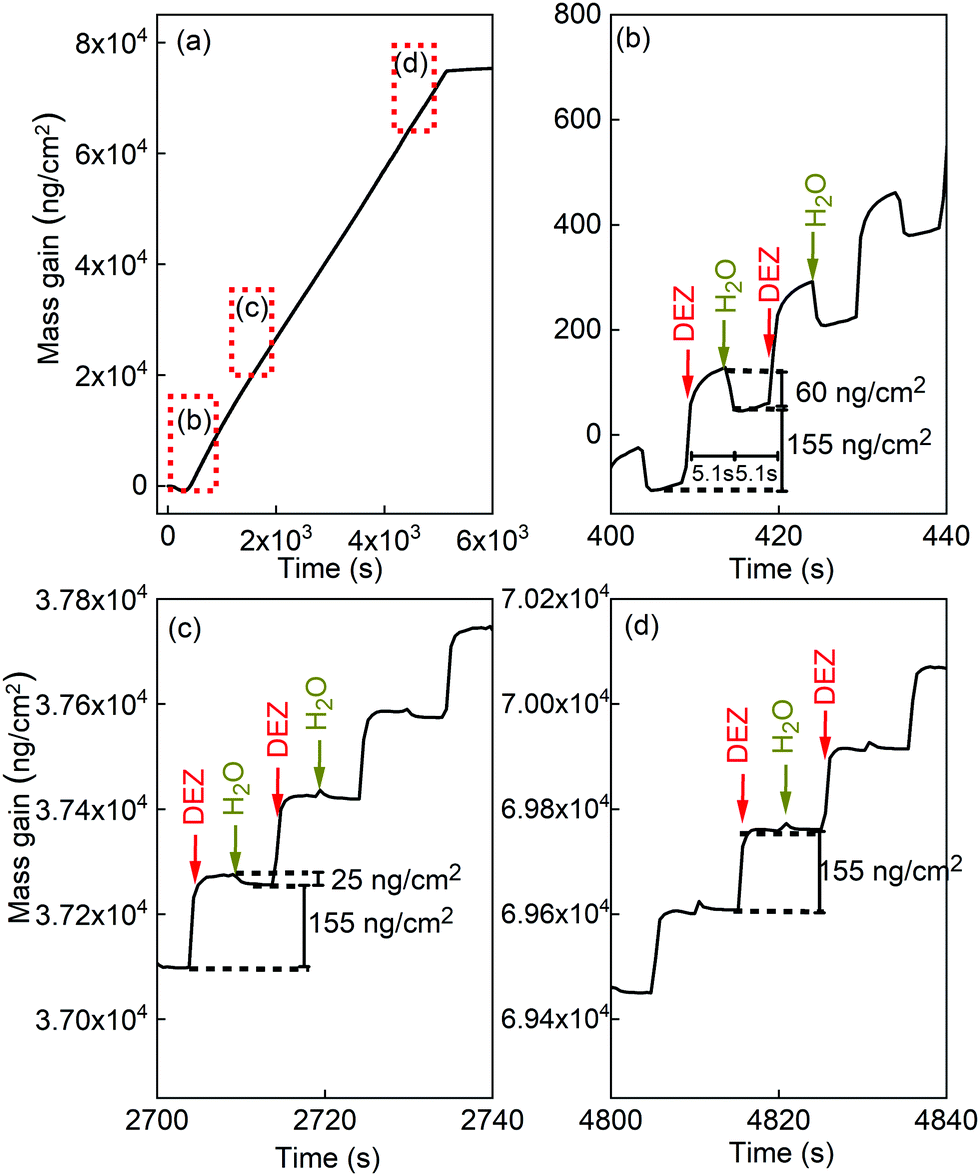 | ||
| Fig. 3 In situ QCM growth characteristics of the ZnO thin film grown without O2; (a) a completed growth process, (b)–(d) enlargements of QCM characteristics at different moments of the growth, as indicated in the graph (a). | ||
The in situ QCM characteristics of the ZnO thin film synthesized in the presence of oxygen gas are shown in Fig. 4. The timing sequence is written as 0.1 s (DEZ pulsing)–5 s (Ar purging)–1 s (O2 pulsing)–20 s (Ar purging)–0.1 s (18O-labeled DI water pulsing)–10 s (Ar purging).
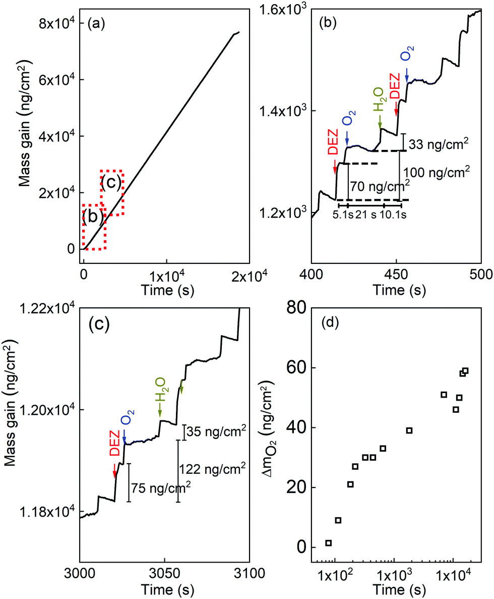 | ||
| Fig. 4 In situ QCM growth characteristics of the ZnO thin film grown with O2; (a) a completed growth process, (b) and (c) enlarged views of QCM characteristics at different moments of the growth, as indicated in (a), and (d) mass gain after the oxygen pulse as a function of deposition time. | ||
Here also, the whole growth processes present a linear dependence of the mass gain on deposition time, as shown in Fig. 4(a). Enlarged views of the QCM results that highlight the growth characteristics of the ZnO film at indicated periods are shown in Fig. 4(b) and (c). After the first 3000 s, corresponding to 80 cycles, the steady-state in mass gain is achieved during the ALD loop stages for DEZ pulsing, inserted oxygen exposures, and water pulsing. The mass gain for the DEZ, oxygen gas, and H2O exposures is ΔmDEZ ≈ 70–75 ng cm−2, ΔmO2 ≈ 30–47 ng cm−2, ΔmH2O ≈ 33–35 ng cm−2, respectively. The total mass gain per cycle is Δm ≈ 133–157 ng cm−2. It is worth mentioning that the mass gain after the oxygen pulse rises as the deposition time increases, as presented in Fig. 4(d). Moreover, a positive mass change during the water pulse was observed instead of a negative one for the ALD process without oxygen gas.
3.3. D-SIMS and ToF-SIMS analysis of the ALD ZnO thin films
D-SIMS analysis was used to trace the contribution of each source of oxygen atoms: 18O from the DI water precursor, and 16O from the O2 gas pulsing during the ALD cycles. Fig. 5(a) and (b) present the SIMS depth profiles of both ZnO films. A higher amount of oxygen is observed in the film grown with gaseous O2, which is in line with the XPS results that showed a secondary peak in the O 1s spectrum and the increase of the O 1s–Zn 4sp hybridized states in the valence band spectra.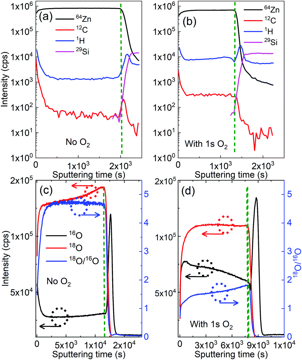 | ||
| Fig. 5 SIMS depth-profile acquired with a Cs+ bombardment of ZnO thin films grown (a) without and (b) with O2 gas, oxygen isotopic signatures determined with the M− mode analysis of ZnO thin films synthesized (c) without and (d) with gaseous O2. The olive short dash lines indicate the transition between films (the left sides) and silicon substrates (the right sides). | ||
Fig. 5(c) and (d) show that the depth-resolved SIMS analysis of 18O originated predominantly from the 18O-enriched water (H218O), 16O stemmed mainly from oxygen gas, and the 18O/16O ratio for ZnO thin films grown with and without an additional presence of oxygen gas, respectively. On one hand, the 18O/16O ratio remains unchanged at around 4.7 versus the sputtering time for the film grown with DEZ and water only. The 18O/16O obtained value of 4.7 is significantly small compared to the 18O/16O ratio of 18O-labeled deionized water of 32. This is due to a dilution effect as the introduction of H218O is done in the reaction chamber with certain levels of residual gases and moisture (the chamber pressure of approximately 1.2 mbar) where 16O predominates (16O: 99.757% and 18O: 0.205%, i.e.18O/16O ∼2.05 × 10⁻³). Consequently, the 18O/16O ratio of the ZnO film drastically decreases. On the other hand, it decreases from a value of 1.8 to 1.5 as the film grows (i.e. towards the low value of sputtering time) with the additional O2.
This decrease in the 18O/16O ratio upon the sputtering time implies that the oxygen atoms mainly stem from water at the early stage of the growth, meaning that the contribution of the water precursor is predominant. However, the contribution of additional O2 gas in the growth process gradually becomes significant as the film gets thicker. This is in line with the observation from the QCM data (Fig. 4(d)), which shows the increase in the mass gain after the O2 pulse. It is also worth noticing that amounts of carbon and hydrogen present in bulk in the ZnO film grown with O2 are about 50% higher than those of the ZnO film grown without O2 (Fig. 5(a) and (b)). This will be commented on later in the discussion.
Fig. 6 presents the ToF-SIMS analysis of the ZnO thin films. ZnxOyH− ions are detected for both ZnO thin films due to the fact that the films were grown by using DEZ and DI water as precursors. Interestingly, ZnxOyC2H5− ions are only detected in the ZnO films grown in the presence of gaseous O2. This signature suggests a direct chemical reaction of the O2 gas molecules with the growing ZnO-based thin film during the ALD process. This is also supported by the lower 18O/16O ratios measured (Fig. 5c and d) through the whole thickness of the film with the additional presence of O2 during the ALD process. It is also noticing that the presences of Cl−, NO3−, SO42−, and fluor were observed. The presences of these ions can be due to contaminants on the surface, which were not detected by XPS because its sensitivity is lower than dynamic or ToF-SIMS.
 | ||
| Fig. 6 TOF-SIMS spectra with the m/z ranges of (a) 0–200, (b) 200–400, (c) 400–600, and (d) 600–800 acquired by negative mode of ZnO thin films grown with (red) and without (blue) O2 gas. | ||
A high resolution lateral mapping by HIM-SIMS of the 18O and 16O atoms, and respective overlaps of (18O + 16O), on Fig. S1 (in the ESI†) show a uniform distribution of both atoms among the structure of the grains, depicted in Fig. 1, of the polycrystalline ZnO thin films synthesized with and without 1 s of oxygen gas pulsing for each ALD loop.
4. Discussion
The present study confirms and complements our previous work,17 by showing how the presence of oxygen gas pulsing during the ALD process profoundly affects the crystallographic, morphological, optical, electrical, and electronic properties of ZnO thin films (Fig. 1, 2 and Fig. S2, S3 in the ESI†). In particular, the crystal structure of ZnO thin film changed to a polycrystalline structure with a highly preferred (002) orientation as oxygen gas pulsing was applied at 180 and 200 °C. Compared to ZnO films grown using only DEZ and water, the electrical resistivity of ZnO thin film increased by 3 to 4 orders of magnitude for the films grown at 180 and 100 °C in the presence of oxygen gas pulsing, respectively (Fig. S3 in the ESI†). Complementary to our first work17 highlighting the impact of the oxygen gas presence in the growth process on the properties of ZnO films, in this study, we point out that these profound features are in intimate correlation with the oxygen chemisorption incorporated in the ZnO surface during growth, which is identified by the XPS analysis showing an additional peak at 532.2 eV, allocated to hydroxides, and an increase of the O 2p–Zn 4sp hybridized states in the valence bands, due to the incorporation of O and/or OH in the ZnO films. By chemisorbing oxygen, the ZnO(001)–Zn polar surface can be electrostatically stabilized as highlighted by P. Gorai et al.34 Thus, the (002) orientation films grew preferentially. In addition, it was found that the native defects, mainly oxygen vacancies, decreased by absorbing oxygen molecules,17 resulting in an increase in resistivity.For ZnO film growth using DEZ and water precursors, the reaction mechanism usually follows the reactions (R2a) and (R3). If all hydroxyl groups are linked to MEZ groups after the DEZ saturation, the mass change during the water pulse should be negative as the ethyl ligands are replaced by much lighter hydroxyl groups via the ligand-exchange reaction. For the first 266 cycles of growth (about 2700 s of growth duration), the reaction mechanism follows reactions (R2a) and (R3), as shown in Fig. 3(b) and (c). After that, the non-negative mass change during the water pulse was observed (Fig. 3(c) and (d)). This behavior was also reported by Yousfi and co-workers.20 It suggests that the reaction mechanism postulated in equations (R2a) and (R3) does not completely reflect the nature of the growth process. It is possible that after reactions (R2a) and (R2b) can also occur, thus leading to the presence of bare zinc atoms in addition to the monoethyl zinc on the surface.18,35 These bare zinc atoms can adsorb more water onto the surface and counterbalance the mass change due to the ligand-exchange reaction. T. Weckman and K. Laasonen proposed this explanation based on density functional theory study on the atomic layer deposition of zinc oxide and supported by experimental results from other publications.18,35 The surface ethyl-ligand elimination during the water pulse is incomplete, resulting in persisting ethyl ligands on the surface after the water pulse has ended. The fraction of these persisting ligands is strongly dependent on temperature, suggesting that there is a kinetic barrier to ligand elimination by water. At elevated temperatures the kinetic barrier for the ligand removal is overcome, and the number of persisting ligands can be expected to be reduced as a function of temperature. As the surface becomes rapidly saturated with monoethyl zinc, the adsorption of diethyl zinc slows and the monoethyl zinc slowly reacts with the remaining hydroxyl groups into bare zinc atoms. In addition, the effect of surface morphology on the ligand-exchange reactions have been theoretically studied.35 Their calculation suggested that the initial ligand-exchange reactions are preferred on the planar surface over the step surface. Yousfi et al.20 also discussed that a film crystal structure might have invoked the change of growth mechanisms due to polar (002) and non-polar (100) planes. Therefore, as the film grew the film structure and morphology can be changed. These may contribute to the change of the reaction mechanisms.
In the presence of oxygen gas during the ALD growth, the growth characteristic is completely different from the one grown by DEZ and water precursors only, as shown in Fig. 4. Ignatyev et al.36 and Rienstra-Kiracofe et al.37 demonstrated that the monoethyl radical could react to O2 in the event of the additional presence of gaseous O2 during ALD processes to form the ethylperoxy radical:
| C2H5˙ + O2 → CH3CH2OO˙ | (R4) |
| I–O–Zn–C2H5 + O2 → I–O–Zn–C2H5O2 | (R2c) |
A higher intensity of carbon and hydrogen by D-SIMS in the film grown with O2 compared to the film grown without O2 and particularly the significant detection of ZnxOyC2H5− ion by TOF-SIMS supports our hypothesis. As a result, the formation of ethylperoxy groups induces the positive mass change during the gaseous O2 pulse. Possibly, reactions (R2b) and (R2c) occur simultaneously, leading to the presence of zinc atoms and the formation of I–O–Zn–C2H5O2. As pointed out by D. H. Ehhalt et al.,38 the ethylperoxy radical is polar, relatively long-lived and water-reactive. This form of Criegee intermediate is known to have a very high reactivity with water vapor to form mainly alkylhydroperoxides.39 L. Sheps et al. also determined the additional minor formation of aldehydes and carboxylic acids.40 Hence, these ethylperoxy radical formations would cause more adsorption of water during the water pulse in the ALD cycle to form mainly ethylhydroperoxide chains, resulting in the positive mass change during the water pulse, which is consistent to the in situ QCM data (Fig. 4). A quantitative estimation of the incorporation of oxygen atoms from H2O and O2 by the D-SIMS measurements of the 18O/16O ratio in Fig. 5 would deserve a more complete analysis of the final end products reaction rates of the Criegee intermediates with water during growth of the film with steric interactions to consider and not treated in this work.
5. Conclusions
The use of 18O-labelled isotopic water as precursor to track the origin of oxygen atoms in ZnO film from two different sources is an original and powerful approach to conclusively demonstrate that the presence of additional gaseous O2 in the atomic layer deposition (ALD) process causes a new chemical reaction mechanism in the growth of ZnO thin film, modifying its properties. The detection of ZnxOyC2H5− ions accompanied by the in situ quartz crystal microbalance characteristics suggests a new reaction mechanism in the ZnO thin films grown with O2 gas presence, i.e. monoethyl zinc reacts further with O2, leading to the positive mass changes during the O2 and water pulses by the respective formation of ethylperoxy radicals and ethylhydroperoxide chains in the bulk of the film. The monitoring of the 18O/16O ratio along the depth of the film highlighted the evolution of the chemical contribution of the water precursor and gaseous O2 during the ALD growth. It is shown, when coupling the water precursor with gaseous O2 in the ALD process, that the gaseous O2 contribution of the oxygen atoms in the chemistry of the thin film continuously increases during the growth process. D-SIMS and XPS results have also proven that additional oxygen species are present in the ZnO films when gaseous O2 is added in the ALD process. The increase of the O 2p–Zn 4sp hybridized states in the valence band, observed when oxygen gas was added during the synthesis process, corresponds to a decrease of the oxygen vacancies density in the film, leading to the drop of the electrical conductivity. As another consequence, the green emission band is suppressed due to the presence of added oxygen inside the ZnO film that counter-balances the formation of oxygen vacancies.Data availability
The raw/processed data required to reproduce these findings can be shared on reasonable request.Authorship contribution statement
The manuscript was written with contributions from all authors. All authors have given their approval to the final version of the manuscript.Credit authorship contribution statement
Tai Nguyen: methodology, experiments (ALD processes, characterizations), data acquisition and analysis, manuscript writing – original draft. Nathalie Valle: methodology, experiments (SIMS), data analysis and interpretation, review and editing. Jérôme Guillot: XPS analysis and data interpretation, review & editing. Jérôme Bour: ToF-SIMS acquisition and analysis. Noureddine Adjeroud: methodology, experiments (ALD processes). Yves Fleming: XRD experiments and data analysis interpretation, review & editing. Mael Guennou: photoluminescence analysis and data interpretation, review & editing. Jean-Nicolas Audinot: methodology, experiments (HIM-SIMS), data analysis, and interpretation. Brahime El Adib: experiments (SIMS), data analysis. Raoul Joly: experiments (ALD processes, characterizations). Didier Arl: SEM analysis and data interpretation, review & editing. Gilles Frache: ToF-SIMS analysis. Jérôme Polesel Maris: project manager, supervisor, ALD experiments, data analysis, funding acquisition, manuscript writing, review & editing.Conflicts of interest
The authors declare that there are no competing interests.Acknowledgements
The authors acknowledge Dr Petru Lunca Popa for his support on optical spectra measurements. The authors gratefully acknowledge the financial assistance provided by the FNR in the framework of the FNR CORE project PSSENS (Project ref. PSSENS C16/MS/11349047) and the FNR PRIDE MASSENA 15/10935404/MASSENA for funding.References
- Y. S. Choi, J. W. Kang, D. K. Hwang and S. J. Park, Recent Advances in ZnO-Based Light-Emitting Diodes, IEEE Trans. Electron Devices, 2010, 57, 26–41 CAS.
- R. S. Mane, W. J. Lee, H. M. Pathan and S. H. Han, Nanocrystalline TiO2/ZnO Thin Films: Fabrication and Application to Dye-Sensitized Solar Cells, J. Phys. Chem. B, 2005, 51, 24254–24259 CrossRef PubMed.
- T. Van Dang, N. Duc Hoa, N. Van Duy and N. Van Hieu, Chlorine Gas Sensing Performance of On-Chip Grown ZnO, WO3, and SnO2 Nanowire Sensors, ACS Appl. Mater. Interfaces, 2016, 8(7), 4828–4837 CrossRef CAS PubMed.
- L. Le Brizoual, F. Sarry, O. Elmazria, P. Alnot, S. Ballandras and T. Pastureaud, GHz Frequency ZnO/Si SAW Device, IEEE Trans. Ultrason. Eng., 2008, 55, 442–450 Search PubMed.
- Z. L. Wang and J. Song, Piezoelectric Nanogenerators Based on Zinc Oxide Nanowire Arrays, Science, 2006, 312, 242–246 CrossRef CAS PubMed.
- R. Hinchet, S. Lee, G. Ardila, L. Montès, M. Mouis and Z. L. Wang, Performance Optimization of Vertical Nanowire-Based Piezoelectric Nanogenerators, Adv. Funct. Mater., 2014, 24, 971–977 CrossRef CAS.
- R. Joly, S. Girod, N. Adjeroud, T. Nguyen, P. Grysan, S. Klein, K. Menguelti, C. Vergne and J. Polesel-Maris, Polymeric Cantilevered Piezotronic Strain Microsensors Processed by Atomic Layer Deposition, Sens. Actuators, A, 2020, 315, 112280 CrossRef CAS.
- E. Bellingeri, D. Marré, I. Pallecchi, L. Pellegrino, G. Canu and A. S. Siri, Deposition of ZnO Thin Films on SrTiO3 Single-Crystal Substrates and Field Effect Experiments, Thin Solid Films, 2005, 486, 186–190 CrossRef CAS.
- K. Matsubara, P. Fons, A. Yamada, M. Watanabe and S. Niki, Epitaxial Growth of ZnO Thin Films on LiNbO3 Substrates, Thin Solid Films, 1999, 347, 238–240 CrossRef CAS.
- H. F. Liu, S. J. Chua, G. X. Hu, H. Gong and N. Xiang, Effects of Substrate on the Structure and Orientation of ZnO Thin Film Grown by Rf-Magnetron Sputtering, J. Appl. Phys., 2007, 102, 083529 CrossRef.
- M. Novotný, J. Cižék, R. Kužel, J. Bulíř, J. Lančok, J. Connolly, E. McCarthy, S. Krishnamurthy, J. P. Mosnier and W. Anwand, et al., Structural Characterization of ZnO Thin Films Grown on Various Substrates by Pulsed Laser Deposition, J. Phys. D: Appl. Phys., 2012, 45, 225101 CrossRef.
- S. J. Kang and Y. H. Joung, Influence of Substrate Temperature on the Optical and Piezoelectric Properties of ZnO Thin Films Deposited by Rf Magnetron Sputtering, Appl. Surf. Sci., 2007, 253, 7330–7335 CrossRef CAS.
- A. M. Rosa, Da Silva, E. P. Amorim, E. Chaves, M. Catto, A. C. Lisboa-Filho, P. N. Bortoleto and J. R. R. Growth, Evolution of ZnO Thin Films Deposited by RF Magnetron Sputtering, J. Phys.: Conf. Ser., 2012, 370, 012020 CrossRef.
- J. Husna, M. Mannir Aliyu, M. Aminul Islam, P. Chelvanathan, N. Radhwa Hamzah, M. Sharafat Hossain, M. R. Karim and N. Amin, Influence of Annealing Temperature on the Properties of ZnO Thin Films Grown by Sputtering, Energy Procedia, 2012, 25, 55–61 CrossRef CAS.
- F. H. Wang and C. L. Chang, Effect of Substrate Temperature on Transparent Conducting Al and F Co-Doped ZnO Thin Films Prepared by Rf Magnetron Sputtering, Appl. Surf. Sci., 2016, 370, 83–91 CrossRef CAS.
- S. H. K. Park and Y. E. Lee, Controlling Preferred Orientation of ZnO Thin Films by Atomic Layer Deposition, J. Mater. Sci., 2004, 39, 2195–2197 CrossRef.
- T. Nguyen, N. Adjeroud, M. Guennou, J. Guillot, Y. Fleming, A.-M. Papon, D. Arl, K. Menguelti, R. Joly and N. Gambacorti, et al., Controlling Electrical and Optical Properties of Zinc Oxide Thin Films Grown by Thermal Atomic Layer Deposition with Oxygen Gas, Results Mater., 2020, 6, 100088 CrossRef.
- T. Weckman and K. Laasonen, Atomic Layer Deposition of Zinc Oxide: Study on the Water Pulse Reactions from First-Principles, J. Phys. Chem. C, 2018, 122, 7685–7694 CrossRef CAS PubMed.
- T. Weckman and K. Laasonen, Atomic Layer Deposition of Zinc Oxide: Diethyl Zinc Reactions and Surface Saturation from First-Principles, J. Phys. Chem. C, 2016, 120(38), 21460–21471 CrossRef CAS.
- E. B. Yousfi, J. Fouache and D. Lincot, Study of Atomic Layer Epitaxy of Zinc Oxide by In Situ Quartz Crystal Microgravimetry, Appl. Surf. Sci., 2000, 153, 223–234 CrossRef CAS.
- T. Wirtz, De Castro, O. Audinot, J.-N. Philipp and P. Imaging, and Analytics on the Helium Ion Microscope, Annu. Rev. Anal. Chem., 2019, 12, 523–543 CrossRef CAS PubMed.
- D. Dowsett and T. Wirtz, Co-Registered in Situ Secondary Electron and Mass Spectral Imaging on the Helium Ion Microscope Demonstrated Using Lithium Titanate and Magnesium Oxide Nanoparticles, Anal. Chem., 2017, 89(17), 8957–8965 CrossRef CAS PubMed.
- B. D. Viezbicke, S. Patel, B. E. Davis and D. P. Birnie, Evaluation of the Tauc Method for Optical Absorption Edge Determination: ZnO Thin Films as a Model System, Phys. Status Solidi B, 2015, 252, 1700–1710 CrossRef CAS.
- A. B. Djurišić, Y. H. Leung, K. H. Tam, Y. F. Hsu, L. Ding, W. K. Ge, Y. C. Zhong, K. S. Wong, W. K. Chan and H. L. Tam, et al., Defect Emissions in ZnO Nanostructures, Nanotechnology, 2007, 18, 095702 CrossRef.
- B. Panigrahy, M. Aslam, D. S. Misra, M. Ghosh and D. Bahadur, Defect-Related Emissions and Magnetization Properties of ZnO Nanorods, Adv. Funct. Mater., 2010, 20, 1161–1165 CrossRef CAS.
- O. Lupan, T. Pauporté, L. Chow, B. Viana, F. Pellé, L. K. Ono, B. Roldan Cuenya and H. Heinrich, Effects of Annealing on Properties of ZnO Thin Films Prepared by Electrochemical Deposition in Chloride Medium, Appl. Surf. Sci., 2010, 256, 1895–1907 CrossRef CAS.
- M. A. Thomas and J. B. Cui, Highly Tunable Electrical Properties in Undoped ZnO Grown by Plasma Enhanced Thermal-Atomic Layer Deposition, ACS Appl. Mater., 2012, 4, 3122–3128 CrossRef CAS PubMed.
- S. Bang, S. Lee, J. Park, S. Park, Y. Ko, C. Choi, H. Chang, H. Park and H. Jeon, The Effects of Post-Annealing on the Performance of ZnO Thin Film Transistors, Thin Solid Films, 2011, 519(22), 8109–8113 CrossRef CAS.
- N. Kamarulzaman, M. F. Kasim and N. F. Chayed, Elucidation of the Highest Valence Band and Lowest Conduction Band Shifts Using XPS for ZnO and Zn0.99Cu0.01O Band Gap Changes, Results Phys., 2016, 6, 217–230 CrossRef.
- B. J. Coppa, R. F. Davis and R. J. Nemanich, Gold Schottky Contacts on Oxygen Plasma-Treated, n-Type ZnO(000
![[1 with combining macron]](https://www.rsc.org/images/entities/char_0031_0304.gif) ), Appl. Phys. Lett., 2003, 82, 400 CrossRef CAS.
), Appl. Phys. Lett., 2003, 82, 400 CrossRef CAS. - K. Sawada, Y. Shirotori, K. Ozawa, K. Edamoto and M. Nakatake, Valence Band Structure of the ZnO(100) Surface Studied by Angle-Resolved Photoemission Spectroscopy, Appl. Surf. Sci., 2004, 237, 343–347 CrossRef CAS.
- M. J. Al-Saadi, S. H. Al-Harthi, H. H. Kyaw, M. T. Z. Myint, T. Bora, K. Laxman, A. Al-Hinai and J. Dutta, Influence of Atomic Hydrogen, Band Bending, and Defects in the Top Few Nanometers of Hydrothermally Prepared Zinc Oxide Nanorods, Nanoscale Res. Lett., 2017, 12, 22 CrossRef PubMed.
- J. W. Chiou, S. C. Ray, H. M. Tsai, C. W. Pao, F. Z. Chien, W. F. Pong, M. H. Tsai, J. J. Wu, C. H. Tseng and C. H. Chen, et al., Charge Transfer in Nanocrystalline-AuZnO Nanorods Investigated by X-Ray Spectroscopy and Scanning Photoelectron Microscopy, Appl. Phys. Lett., 2007, 92, 192112 CrossRef.
- P. Gorai, E. G. Seebauer and E. Ertekin, Mechanism and Energetics of O and O2 Adsorption on Polar and Non-Polar ZnO Surfaces, J. Chem. Phys., 2016, 144, 184708 CrossRef PubMed.
- T. Weckman and K. Laasonen, Atomic Layer Deposition of Zinc Oxide: Diethyl Zinc Reactions and Surface Saturation from First-Principles, J. Phys. Chem. C, 2016, 120, 21460–21471 CrossRef CAS.
- I. S. Ignatyev, Y. Xie, W. D. Allen and H. F. Schaefer, Mechanism of the C2H5 + O2 Reaction, J. Chem. Phys., 1997, 107, 141 CrossRef CAS.
- J. C. Rienstra-Kiracofe, W. D. Allen and H. F. Schaefer, C2H5 + O2 Reaction Mechanism: High-Level Ab Initio Characterizations, J. Phys. Chem. A, 2000, 144, 9823 CrossRef.
- W. Jaeschke, Multiphase Atmospheric Chemistry, Chemistry of Multiphase Atmospheric Systems, Springer, Berlin, Heidelberg, 1986, vol. 6 Search PubMed.
- W. Chao, J. T. Hsieh, C. H. Chang and J. J. M. Lin, Direct Kinetic Measurement of the Reaction of the Simplest Criegee Intermediate with Water Vapor, Science, 2015, 347, 751–754 CrossRef CAS.
- L. Sheps, B. Rotavera, L. A. Eskola, L. D. Osborn, A. C. Taatjes, K. Au, E. D. Shallcross, H. M. A. Khan and J. C. Percival, The reaction of Criegee Intermediate CH2OO with Water Dimer: Primary Products and Atmospheric Impact, Phys. Chem. Chem. Phys., 2017, 19, 21970–21979 RSC.
Footnote |
| † Electronic supplementary information (ESI) available: Additional information with complementary data concerning XRD spectra, the ZnO thin film grown with and without oxygen gas at different deposition temperatures, electrical resistivity of ZnO thin films, and HIM–SIMS mapping. See DOI: 10.1039/d0tc05439a |
| This journal is © The Royal Society of Chemistry 2021 |