
 Open Access Article
 This Open Access Article is licensed under a Creative Commons Attribution-Non Commercial 3.0 Unported Licence
Photoluminescence emission induced by localized states in halide-passivated colloidal two-dimensional WS2 nanoflakes†
Rosanna
Mastria
 *a,
Anna
Loiudice
b,
Jan
Vávra
b,
Concetta
Nobile
a,
Riccardo
Scarfiello
a,
P. Davide
Cozzoli
cd,
Alessandro
Kovtun
e,
Andrea
Liscio
f,
Nicola
Sestu
g,
Daniela
Marongiu
g,
Francesco
Quochi
g,
Raffaella
Buonsanti
b,
Michele
Saba
g,
Arrigo
Calzolari
h and
Aurora
Rizzo
*a
*a,
Anna
Loiudice
b,
Jan
Vávra
b,
Concetta
Nobile
a,
Riccardo
Scarfiello
a,
P. Davide
Cozzoli
cd,
Alessandro
Kovtun
e,
Andrea
Liscio
f,
Nicola
Sestu
g,
Daniela
Marongiu
g,
Francesco
Quochi
g,
Raffaella
Buonsanti
b,
Michele
Saba
g,
Arrigo
Calzolari
h and
Aurora
Rizzo
*a
aCNR NANOTEC – Institute of Nanotechnology, Polo di Nanotecnologia, c/o Campus Ecotekne, Via Monteroni, 73100 Lecce, Italy. E-mail: aurora.rizzo@nanotec.cnr.it; rosanna.mastria@nanotec.cnr.it; Tel: +39 0832 319816 Tel: +39 0832 319101
bLaboratory of Nanochemistry for Energy (LNCE), Department of Chemical Sciences and Engineering, École Polytechnique Fédérale de Lausanne, Sion, CH-1950, Switzerland
cDipartimento di Matematica e Fisica “E. De Giorgi”, Università del Salento, Via per Arnesano, 73100 Lecce, Italy
dUdR INSTM di Lecce, c/o, Università del Salento, Campus Ecotekne, via Arnesano, 73100 Lecce, Italy
eCNR ISOF – Institute for the Organic Synthesis and Photoreactivity, via Gobetti 101, 40129, Bologna, Italy
fInstitute of Microelectronics and Microsystems (IMM), National Research Council of Italy (CNR), via del Fosso del Cavaliere 100, 00133 Rome, Italy
gDipartimento di Fisica, Università di Cagliari, I-09042 Monserrato, Italy
hIstituto Nanoscienze, CNR-NANO, S3 Center, Via Campi 213/a, 41125 Modena, Italy
First published on 12th January 2021
Abstract
Engineering physicochemical properties of two-dimensional transition metal dichalcogenide (2D-TMD) materials by surface manipulation is essential to enabling their practical and large-scale application. This is especially challenging for colloidal 2D-TMDs that are plagued by the unintentional formation of structural defects during the synthetic procedure. However, the available methods to manage surface states of 2D-TMDs in solution phase are still limited, hampering the production of high-quality colloidal 2D-TMD inks. Here, we demonstrate an efficient solution-phase strategy to passivate surface defect states of colloidal WS2 nanoflakes with halide ligands, which results in the activation of their photoluminescence emission. Photophysical investigation and density functional theory calculations suggest that halide atoms enable the suppression of non-radiative recombination through the elimination of deep gap trap states and the introduction of localized states in the energy band structure from which excitons can efficiently recombine. Importantly, halide passivated WS2 nanoflakes retain colloidal stability and photoluminescence emission after several weeks of storage in ambient atmosphere, corroborating the potential of developed WS2 inks thereof.
Introduction
Two-dimensional transition metal dichalcogenides are at the forefront of materials science research and technology.1–4 Composition, thickness, structure and surface chemistry of 2D-TMDs affect their physical and chemical properties, providing opportunities to design and engineer semiconductor materials that meet requirements for specific applications.5–8 Herein, advances in solution-based synthetic approaches have opened the way towards large-scale and low-cost production of inks consisting of 2D-TMDs that can be potentially printed or embedded into functional films or composites in a facile and straightforward way.9–12 Liquid-phase exfoliation can easily produce a wide range of 2D-TMD inks at low cost, but the limited control over the exfoliation process results in a broad distribution of crystal thickness and lateral dimension. This calls for tedious post production process (i.e. gradient centrifugation) to improve the monodispersity of the sample.13,14 Surfactant-assisted colloidal approaches for 2D-TMD synthesis, although still in their early stages of development, provide key advantages over other existing methods since they require mild synthetic conditions while allowing precise control over 2D-TMD composition, geometry, and crystal structure.15,16 To date, colloidal approach has been proven successful to synthesize a wide range of solution-processable 2D-TMDs with mono- to few-layer thicknesses,17 controlled lateral size,18 and crystal phase.19,20 The photophysical properties of colloidal 2D-TMDs are still nearly unexplored and the impact of structural defect and/or defect engineering on their optical and electronic properties is poorly understood, hampering the widespread application of this promising synthetic approach.21In general, 2D-TMDs synthesized by colloidal approach are characterized by ultrafast non-radiative recombination and extremely poor photoluminescence quantum yield (PLQY) at room temperature. Photoluminescence (PL) suppression in nanostructures with large surface-to-volume ratio is often ascribed to non-radiative Auger recombination promoted by charge trapping on defects at the surface.22–24 In colloidal 2D-TMDs, due to the volatile nature of chalcogen precursor used for the synthesis, such defects mainly consist of chalcogen vacancies18,25 that are responsible for the appearance of deep in-gap energy levels causing non-radiative electron–hole recombination.26,27 The high density of chalcogen vacancies hinders the extensive use of colloidal 2D-TMDs in optoelectronic platforms, for which it is essential to develop an effective strategy to engineer defects and to suppress in-gap trap states.
Defect-chemistry manipulation is a powerful tool to manage the extended surface of 2D-TMDs, to heal defects and therefore to control the structure of energy levels, enabling future opportunities for optoelectronic device applications.6,28 Furthermore, substituents play an important role in 2D-TMD recombination processes creating localization centres that are responsible of a large number of localization-induced optical phenomena that could be exploited to further engineer the optical response of colloidal 2D-TMDs.29 In previous reports, passivation of chalcogen vacancies of CVD grown or mechanically exfoliated 2D-TMDs have been achieved by performing post-deposition treatments with superacid molecules or hydrohalic acid, which are able to fill chalcogen vacancies, thereby.30,31 However, such post deposition approaches preclude solution processability of passivated colloidal 2D-TMDs as well as any possibility of scalability. On the other hand, solution-phase passivation protocols developed for metal chalcogenides colloidal quantum dots are not effective for 2D-TMDs because of their different structures: 2D-TMDs are characterised by chalcogen-rich surfaces, hence, unsaturated metal cations are not exposed to the external environment, while metal–chalcogenide quantum dots typically exhibit metal-rich surfaces that are directly chemically accessible.32,33
Here, we target the issue of chalcogen vacancies, which negatively affect optical properties of colloidal 2D-TMDs, to finally obtain higher PLQY and long PL lifetime in colloidal WS2 nanoflakes (NFs). Among the 2D-TMDs family, WS2 represents a promising component and a valid alternative to the most studied Mo counterpart.34,35 Similarly to MoS2 and other 2D-TMDs, approaching the mono-to-few-layer size limit, WS2 accommodate indirect-to-direct bandgap transitions36,37 and a decrease in dielectric screening,38 which result in an optical response dominated by excitons with strong Coulomb interaction and large binding energy.39 Additionally, WS2 exhibits a unique combination of appealing optical and electronic features such as giant spin–orbit coupling splitting,40 biexciton emission,41 and single photon-emission42 to list a few, which are highly sought for optoelectronics and nanophotonics.
We explore monovalent halide ligands to passivate sulfur vacancies in colloidal WS2 nanoflakes (NFs), while preserving their colloidal stability and solution processability (Fig. 1). By exploiting the strong affinity of halide ligands toward metal cations as well as their ability to reach recessed sites within individual few-layer-thick flakes due to their small size,43,44 we effectively passivate unsaturated metal atoms allowing the activation of PL emission that otherwise is negligible in the pristine NFs. The investigation of charge-carrier relaxation pathways in halide passivated WS2 NFs, achieved through the combination of photoluminescence excitation (PLE) and time-resolved PL measurements (TRPL), reveals that halide ligands introduce high-energy localized states. Such localized states are responsible for capture events that hinder intervalley scattering and promote high-energy photon emission, thus taking a leading role during recombination processes. Finally, ab initio density functional theory (DFT) simulations elucidate the effect of the halide ligands on the electronic structure of WS2 NFs, and demonstrate that halide atoms act as aliovalent substituents able to saturate dangling bond states originated from chalcogen vacancies and to restore the band gap of the undefective WS2 crystals.
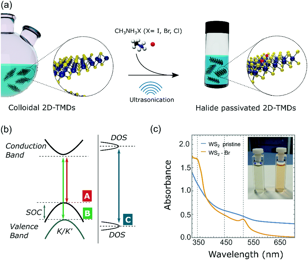 | ||
| Fig. 1 Halide passivation of colloidal WS2 NFs. (a) Schematic illustration of the halide passivation process. (b) Schematic of the optical transitions in WS2. (c) UV-vis absorption spectra of pristine and Br− passivated WS2 NFs after 24 h of sonication; (inset) picture of (left) pristine and (right) Br− passivated WS2 NFs solutions. | ||
Our functionalization approach represents a successful paradigm for the tuning of fundamental properties of colloidal 2D-TMDs. The reported results provide important insights into the understanding of excitonic phenomena associated with defects and defect passivation in colloidal 2D-TMDs.
Results and discussion
Passivation of colloidal WS2 nanoflakes with halide ligands
Colloidal WS2 NFs were synthesized by exploiting an improved sacrificial-conversion route that relied on a solution-phase sulfidation reaction, through which preformed colloidal W18O49 nanorods were converted to WS2 NFs in a suitable surfactant medium.45 The surfactants selected are essential to assist the 2D nucleation and growth of WS2 NFs at the expense of the W18O49 precursor source, allowing the formation of the NFs.15,46 The surfactants are also critical to impart colloidal stability to the NFs minimizing their natural tendency to stack through van der Waals interactions, which has emerged as the major challenge for other liquid-phase preparation methods (e.g. chemical exfoliation). Transmission electron microscopy (TEM) analysis on the as-prepared samples suggests that the final product consists of WS2 bundles, with lateral mean size of about 50 nm, composed of thin single and few-layer WS2 NFs characterized by the coexistence of the metallic 1T’ and the semiconducting 2H crystal structures.12Starting from the as-prepared WS2 NFs (Fig. 2a and b), we performed halide passivation upon mild sonication of a dispersion of NFs in a N-methylformamide (NMF) solution of methylammonium halide salts. After the treatment, the WS2 NFs exhibited very high solubility in NMF (Fig. S1, ESI†) that suggests a mechanism of colloidal stabilization through electrostatic repulsion. Indeed, we expect that negative halide anions bind to unsaturated metal atoms associated with chalcogen vacancies. Rather, methylammonium cations, due to their high solvation energy, act as counterions and form a diffuse layer around the NFs.44,47,48 NMF represents the best choice among the possible solvents for solution stabilization of WS2 NFs since it exhibits an extraordinarily high dielectric constant (ε ∼ 182), essential to stabilize nanocrystals capped with charged inorganic species.44 Importantly, even in the presence of methylammonium halide salts and after prolonged sonication, NMF did not exhibit any sign of incipient degradation and any appreciable PL emission, unlike found in other polar solvents, such as N-methyl-2-pyrrolidone, which show PL after sonication.49 Methylammonium iodide (MAI), methylammonium bromide (MABr), and methylammonium chloride (MACl) were selected as halogen sources to passivate defective colloidal WS2 NFs with I−, Br−, and Cl−, respectively. WS2 NFs passivated with Br− – ions were taken as reference sample due to the intermediate-size atomic radius of Br−. Similar results were obtained with I− and Cl− (see sections ‘Passivation of WS2 nanoflakes with I− ions’ and ‘Passivation of WS2 nanoflakes with Cl− ions’, respectively, in the ESI†).
UV-vis absorption spectra of pristine and Br− passivated colloidal WS2 NFs are reported in Fig. 1c. Like the Br− passivated WS2 NFs, the pristine sample was sonicated in NMF without methylammonium halide salts, to exclude any effect of sonication on the WS2 NF properties. We observed a marked difference in colour appeared between the solutions of the pristine and halide-passivated colloidal WS2 NFs. The diluted solution of pristine WS2 NFs was deep taupe, while the Br−passivated WS2 was orange-reddish (inset in Fig. 1c). The optical absorption of the pristine WS2 NFs was characterized by a broad band in the spectral range between 340 nm and 700 nm without specific optical features (Fig. 1c, blue line). Such behaviour can be attributed to either the mixed semiconducting/metallic phase of WS2 or the large density of defect states.19,50 By contrast, the UV-vis absorption spectra of halide-passivated NFs had two definite absorption peaks located at 340 nm and 510 nm, respectively (Fig. 1c, orange line). After prolonged sonication (42 h, see Fig. S2, ESI†), a weak absorption band at around 440 nm was observed along with an overall broadening of the absorption features. This can be ascribed to an excess of halide atoms engulfed in the crystal structure and/or to an overall damaging of the NFs under protracted sonication, both being detrimental to optical properties. According to previous reports, the optical absorption spectrum of semiconducting 2H WS2 monolayers features two peaks (labelled A and B) arising from two transitions at the K/K′ points, related to the strong spin–orbit coupling that causes a valence band splitting of ∼0.35 eV. A third strong absorption peak (C) at higher energies originates from interband optical transitions across the bandgap (Fig. 1b).36,51,52 Thus, the absorption peaks at 510 and 340 nm are attributable to transitions A and C, respectively, while the lack of well-defined peaks in the optical region where the signature of transition B is expected, (i.e. between A and C), suggests an overlap of several spectral features that hide the B peak.
Optical transitions for our WS2 NFs were blue-shifted compared to those reported in literature for monolayered sheets with lateral size in the micrometre range, but were consistent with 2D-TMDs nanostructures with lower dimensions.17,53–56 The excitonic features of Br− passivated WS2 NFs exhibited broader width than that usually observed in mechanically exfoliated WS2. This is, in part, due to a collective contribution from WS2 NFs randomly oriented in the solution. Low-magnification TEM images of the halide passivated WS2 NFs (Fig. 2c and d) showed that after halide treatment WS2 NFs were organized in bundles randomly oriented with respect to the TEM grid, as for the pristine sample (Fig. 2a and b). A similar morphology was observed independent of the duration of sonication step (Fig. S3, ESI†). Selected-area electron diffraction (SAED) patterns of pristine and Br-passivated WS2 NFs are shown in Fig. 2e, f and the SAED diffractograms are reported in Fig. 2g. The position of major reflections of pristine and Br− passivated colloidal WS2 NFs was similar demonstrating that the crystal structure was mostly retained after the treatment.
 | ||
| Fig. 2 Morphology and composition analyses of pristine and Br− passivated WS2 NFs. TEM images of (a and b) pristine and (c and d) Br− passivated WS2 NFs. The insets depict the planar and vertical orientation of the bundles observed in TEM images. SAED pattern of (e) pristine and (f) Br− passivated WS2 NFs. (g) SAED diffractograms of pristine and Br− passivated WS2 NFs. (h) HAADF-STEM image of the Br− passivated WS2 NFs with the corresponding elemental EDX maps for (i) W, (l) S and (m) Br. | ||
The chemical composition of the colloidal halide passivated WS2 NFs was analysed by energy dispersive X-ray spectrometry (EDX). The corresponding high-angle annular dark field scanning TEM (HAADF-STEM) image in Fig. 2h confirmed that the morphology of the WS2 NFs was retained after the treatment and the bundled structure of the NFs was still clearly observed. W and S atoms were detected, and the stoichiometry of the WS2 NFs was determined to be ∼1![[thin space (1/6-em)]](https://www.rsc.org/images/entities/char_2009.gif) :1.4, which indicates a high density of sulfur vacancies in the pristine sample (see Fig. S4 and Table S1, ESI†). At the same time, elemental mapping revealed the presence of Br in Br-treated WS2 NFs samples, which appeared to be homogenously distributed on the entire NF area (Fig. 2m).
:1.4, which indicates a high density of sulfur vacancies in the pristine sample (see Fig. S4 and Table S1, ESI†). At the same time, elemental mapping revealed the presence of Br in Br-treated WS2 NFs samples, which appeared to be homogenously distributed on the entire NF area (Fig. 2m).
To further support the effectiveness of halide passivation, we compared the EDX spectra of the pristine and halide passivated WS2 NFs samples (Fig. S5, ESI†). The spectra prove the presence of Br atoms on the Br-passivated WS2 NFs, which is quantified in an atomic percentage of 3.9% (see Table S1, ESI†). The EDX spectra did not allow discriminating between the Br bound to the surface or intercalated. Thus, we performed X-Ray Photoemission Spectroscopy (XPS) measurements with the aim to gain insight into the chemical composition of halide passivated WS2 NFs. Fig. 3a and c show the XPS spectra of W 4f and S 2p orbitals in the pristine WS2 NFs sample.
 | ||
| Fig. 3 XPS spectrum of (a and b) W 4f, (c and d) S 2p, and (e) Br 3d signal from pristine and Br− passivated WS2 NFs. | ||
The W 4f XPS spectrum could be decoupled into three distinct doublets: (i) W4+ atoms bounded to sulphide anions (W 4f7/2 ∼ 32.4 eV); (ii) W6+ atoms bound to oxygen in WO3 state (W 4f7/2 ∼ 36.2); (iii) W–O bonds in mixed oxide species (W 4f7/2 at ca. 34.1 eV).12,57 The S 2p XPS spectrum presents only one main peak located at 162.2 eV, which is attributed to S–W bonds in WS2. On comparing the XPS spectra before (as-synthesized) and after mild sonication in NMF without methylammonium halide salts (Fig. S6 and Table S2, ESI†), we could not appreciate significant differences, confirming that mild sonication in NMF did not affect the chemical nature of WS2 NFs.
After halide passivation, the W 4f XPS spectra (Fig. 3b) showed the same feature as those of the pristine sample, with a slight shift to lower binding energies (−0.5 eV) of the doublet associated to WO3. The shift can be appreciated by comparing the fit with fixed binding energy position, where WO3 component can change its binding energy (Fig. S7, ESI†). The observed binding energy shift can be ascribed to the presence of W–Br bounds, expected in the 36.0–37.0 eV region,58 between the W–O and WO3 components. It is noteworthy that a reliable fit could not be achieved only by considering an extra doublet; rather the assessment of W–Br component would require a better signal to noise ratio and resolution of measurements. The S 2p signal in the Br− passivated WS2 NFs (Fig. 3d) presented only S–W chemical state at 162.2 eV and no chemical shift was observed in comparison to the pristine sample. XPS survey of Br 3d in halide passivated WS2 NFs (Fig. 3e) showed a peak at the binding energy of 68.8 eV clearly indicating the presence of ionic Br−. The Br content measured with XPS was in excess respect to the W one (Br/W = 2.7) and was larger than the value measured by EDX (Br/W = 0.1). Taking into account the surface sensitivity of XPS analysis, such evidence strongly suggests the presence of residual MABr on the sample surface.
In general, XPS technique also provide information on the surface doping of semiconductor materials. This information can be obtained analysing three features: (i) the peak shift of the main phase corresponding to the Fermi level change due to adsorbed molecules,59 (ii) the shape of the signal representative of the main phase60 and (iii) the presence of the direct signal from dopant element.60 Considering that there are no examples of XPS analysis for the doping of colloidal TMD materials, herein we refer to doped TMDs prepared by other methods. In a previous report, a slight shift of the Mo 3d signal (+0.2 eV) was observed for Br doped MoSe2 but with only the C 1s calibration and no Fermi energy reference.31 Since the small energy shift on the main phase, reliable XPS measurements could only be obtained by using synchrotron radiation.61 Conversely, significant shifts (0.7–1.1 eV) of the Mo 3d and S 2p signals were reported for MoS2 monolayers produced by sodium-halide assisted CVD methods.62 We cannot however observe the corresponding shift of W 4f and S 2p signals probably due to the different doping approach and the related extent of halide atoms incorporated in the crystal structure.
Nevertheless, in our measurements the analysis of peak shape confirms the Br doping, as shown in change of the shape of W 4f peak due to the W–Br interaction. Overall, XPS analysis indicates the presence of Br dopant without being able a direct assessment of any chemical interaction between WS2 and Br. Nonetheless, comforted by the previous work on MoSe2 doped with Br,31 we suggest that Br 3d peak evidences the presence of an ionic form on the surface which likely fill the chalcogen vacancies present in pristine flakes.31
Localized states in halide passivated WS2 nanoflakes
In order to understand the effectiveness of the halide passivation strategy in suppressing deep gap states, we measured room temperature PL emission from halide passivated WS2 NFs. As-synthesized defective WS2 NFs showed nearly zero-value PL emission, thus preventing any investigation on the electronic bands through PL measurements (Fig. S8, ESI†). When colloidal WS2 NFs were passivated with halide atoms, a noticeable PL in the blue-green region (with PLQY of about 1%) emerged. This agrees with a reduction in the density of deep gap states that otherwise would act as ultrafast non-radiative recombination centres. Indeed, trap states lying deep in the energy gap exhibit a trap depth, defined as the energy difference between the conduction/valence band edges and the defect levels that exceed kBT, where kB and T represent the Boltzmann constant and temperature, respectively. As a result, excited carriers hardly escape from deep traps thus incurring in energy dissipation processes, such as Auger scattering, which finally lead to non-radiative recombination pathways decreasing both the PLQY and the PL lifetime.63Interestingly, halide-passivated WS2 NFs demonstrated to be highly stable, retaining colloidal stability and PL emission after several weeks of storage in ambient atmosphere (Fig. S9, ESI†).
From the analysis of the emission spectra of passivated WS2 NFs, we clearly detected an excitation-wavelength-dependent behaviour of the PL. The emission spectrum underwent to a progressive bathochromic shift as excitation wavelength was increased (Fig. 4a). A similar behaviour is observed in liquid exfoliated WS2 quantum dots, for which size polydispersity induces the PL wavelength emission shift because of different lateral confinement effects.64 However, the well-defined absorption bands in the absorption spectra and the presence of distinctive features in a single PL spectrum suggests the presence of localized electronic states, which could favour the exciton recombination process (see schematic in Fig. 4b).65
 | ||
| Fig. 4 Photoluminescence from Br− passivated WS2 NFs. (a) PL spectra of Br− passivated WS2 NFs at excitation wavelengths of 380 nm (λex1), 430 nm (λex2), and 470 nm (λex3). (b) Schematic of the competing relaxation pathways in halide passivated WS2 NFs. High excitation energies allow charge carriers to access to high-lying localized states from which recombine competing with intervalley scattering and bandgap emission. (c) PLE intensity map. (d) PLE spectra extracted from PLE maps at detection wavelength corresponding to stronger PL emission signals (λem1 = 430 nm, λem2 = 490 nm and λem1 = 530 nm). | ||
In order to probe the spectral origin of the observed emitting states, we performed photoluminescence excitation (PLE) spectroscopy measurements that are summarized in Fig. 4, which shows the PLE intensity map of halide-passivated WS2 NFs after 24 h of sonication (Fig. 4c) along with the PLE spectra at relevant detection wavelengths (Fig. 4d). PLE map highlights three main high-intensity emission signals at 430 nm, 490 nm and 530 nm resulting from excitation wavelength of 380 nm, 430 nm, 470 nm. The PLE spectra, extracted from the PLE map in correspondence of the high intensity emission signals were substantially different from the absorption spectra, discussed above.
Absorption spectra showed only two absorption peaks and a broad absorption band in between, while PLE spectra exhibited distinct peaks providing more information for the study of absorption transitions and related emissive states. The PLE spectrum excited at 430 nm showed a distinctive enhancement in correspondence with the region of the absorption spectra between A and C peaks, precisely at 380 nm, where the lack of distinct peaks in the absorption spectra prevents the unambiguous match between absorption and emission signals. The PLE spectrum at 490 nm reached the maximum intensity at about 430 nm and exhibited two less intense additional peaks at 380 nm and 470 nm. A similar situation was observed in the PLE spectrum at 530 nm that had its maximum at 470 nm and less intense features at 380 nm, 430 nm, and 510 nm, the latter in correspondence with the A transition in the absorption spectrum.
All the above measurements suggest that exciton recombination in our halide passivated WS2 NFs was strongly influenced by localized states. The halide passivation introduce emissive states that competed with intervalley scattering and bandgap emission. In particular, when the samples were excited at high excitation energies, the probability for charge carriers to access and couple to high-energy-lying states is very high. As a result, the emission from the A band was significant only for excitation wavelength just above the band edge.
Finally, we investigated the decay dynamics of the exciton states through TRPL, with the aim to disentangle the mechanisms involved in radiative recombination. TRPL maps obtained with excitation wavelengths of 380 nm, 430 and 470 nm and relative PL decay spectra under the detection wavelength of 530 nm are shown in Fig. 5.
 | ||
| Fig. 5 Exciton radiative decay from Br− passivated WS2 NFs. TRPL emission maps of Br− passivated WS2 NFs for excitation wavelength of (a) 380 nm, (b) 430 nm, (c) 470 nm, respectively; and (d–e–f) relative PL decay transients under detection wavelength at 530 nm. | ||
The spectrograms of the exciton states extracted from the TRPL maps revealed a non-exponential dynamics, with an initial fast decay in the sub-nanosecond range followed by a slower tail with characteristic time on the order of nanoseconds. This suggests that after photoexcitation, most of the excitonic population decayed via a very fast non-radiative recombination through the residual defect states, while some long-lived charge carriers survived trapped at localized states introduced with halide passivation, which slowed down the intervalley relaxation.65,66 This interpretation was further supported by time-resolved spectrograms obtained at different excitation wavelength. Results indicate that the decay became faster as the excitation wavelength approach the band edge, validating the conclusion of a slow intervalley scattering process mediated by localized states. Analogous results were obtained for WS2 NFs passivated with I ions (see Fig. S12 and S13, ESI†) and Cl ions (see Fig. S16 and S17, ESI†).
Restoring of electronic band structure of colloidal WS2 nanoflakes
We used DFT simulations to explore the influence of sulfur vacancies and halide passivation on the electronic structure of WS2 NFs.67 Defect-free, defective, and halide-passivated single layer (1L) WS2 structures modelled by using a (3 × 3) supercell are illustrated in Fig. 6. This relatively small simulation cell was intentionally used to resemble the high defect amount present in the as-grown experimental WS2 samples. The density of states (DOS, Fig. 6b) of a defect-free WS2 monolayer shows a clean band gap without intragap states (bottom panel). The simulated band gap for the extended layer resulted to be 2.1 eV, in very good agreement with the corresponding experimental value (2.03 eV).36,68 The latter value is smaller than the optical bandgap (2.43 eV, i.e. 510 nm) measured here for WS2 NFs, due to the effect of the lateral quantum confinement.67 | ||
| Fig. 6 DFT simulations of Br− passivated WS2 NFs. (a) Modelled defect free, defective and halide passivated WS2 structures. Dashed lines mark the original position of the S vacancies. (b) DOS of the modelled structures. Vertical lines identify the Fermi level (EF) for each system. Gray shaded area indicates the Br-projected contribution (the curve has been magnified ×5 for visual clarity) and black arrows the defect peaks due to S vacancies. | ||
The presence of one or two sulfur vacancies (Svac) in the (3 × 3) supercell, corresponding to 6% (green line) and 12% (pink line) of S defects, respectively, introduces an intragap state near the conduction band (CB) edge. The creation of one S-vacancy (6%) leaves an empty dangling bond state lying deep in the band gap (black arrow), which is responsible for the ultrafast non-radiative recombination of photoexcited excitons discussed above. Vacancy passivation with halide Br atoms (blue line) saturates the defect state and the band gap of the undefective layer is nearly restored. Br acts as aliovalent substituent that saturates the S vacancy and donates its extra p-electron to the host, occupying the bottom of the WS2 conduction bands (n-type degenerate doping), as evident by gray shaded area in Fig. 6.
Increasing the ratio of the incorporated heteroatoms up to very high content (e.g. 12% Br, orange line) does not significantly change this picture, leading only to a shift of the Fermi level deep within the WS2 conduction band. Mixed configuration with Svac and Br ion coexisting in the same sample (e.g. 6% Svac + 6% Br, cyan line) exhibit intermediate behaviour with the effects of the vacancy and of dopant that sum up giving a reduction of the effective band gap (shallow S-derived defect state) and occupation of the bottom of the conduction band (Br charge donation). Note that in this case, the free charge derived by Br dopant partially occupies the lowest Svac defect state (see arrow in Fig. 6). We also investigated the effect of vacancies and halide passivation on WS2 in bilayer configuration by performing DFT calculation for electronic structure. In the bilayer regime, we took into account also the possible intercalation of halide atoms within the bilayer and possible effects arising from the interaction between intercalated atoms and WS2 layers. Intercalation of halide atoms does not have dramatic effect on the electronic structure, namely they just insert and occupy defect state in the host bandgap (see Fig. S18, ESI†). Sulfur vacancies and halide passivation have effects on WS2 bilayer, similar to those observed for the monolayer (see Fig. S19, ESI†).
Conclusions
We have investigated an effective strategy to passivate chalcogen vacancies of colloidal WS2 NFs while preserving colloidal stability. Based on EDX, XPS and DFT results, we propose that halide ligands bind unsaturated metal cations, suppressing deep gap states and nearly restoring the bandgap of defective WS2 to that of a defect-free crystal, which leads to the activation of PL emission. Furthermore, our study reveals that halide passivated WS2 NFs are characterized by the presence of localized surface states that strongly dictate the excited-state relaxation pathways. Our results support the conclusion that in halide-passivated WS2 NFs the presence of localized states hinders the intervalley scattering process promoting radiative recombination before relaxation to the band edge. As a consequence, the vast majority of initial excited states recombine before incurring in intervalley scattering, whereas only a small fraction of them relax to the band edge and recombine, emitting lower energy photons. Indeed, emission from A transition is significant only for excitation wavelengths just above the band edge because the access to localization site is significantly reduced at lower excitation energy.In conclusion, our findings open to the possibility of tailoring optical properties of colloidal 2D-TMDs by exploiting solution-phase passivation approaches. In particular, halide atoms passivate sulfur vacancies, making WS2 NFs bright in photoluminescence, and at the same time introduces localized states that affect optical emission. These results suggest that there is wide scope on developing similar passivation schemes for a wide range of applications, including multicolour biolabeling, display and lasers based on colloidal 2D-TMDs.
Experimental
Materials
1-Octadecene (technical grade 90%), oleylamine (technical grade 70%), oleic acid (technical grade 90%), sulfur (99.998% trace metals basis), NMF (99%) were purchased from Sigma Aldrich and used without further purification. Methylammonium iodide (>99.5%), methylammonium bromide (>99.5%) and methylammonium chloride (>99.5%) were purchased from Lumtec.Synthesis of colloidal WS2 nanoflakes (NFs)
A mixture of 1-octadecene (2.5 mmol) oleylamine (1.25 mmol) and oleic acid (1.25 mmol) is heated to 150 °C and kept under vacuum at this temperature for 1 h to remove impurities such as residual water. Then the mixture was put under nitrogen flow and allowed to cool down to 80 °C. A solution of sub-stoichiometric nanorods in chloroform69 (0.1 mmol of tungsten) was injected, after which the reaction mixture was kept under vacuum for 30 mins to remove chloroform. Then, the temperature was raised to 250 °C and a solution of sulfur in oleylamine (4.5 mg mL−1) was injected dropwise at a rate of 25 μL min−1. After the injection, the resulting mixture was allowed to cool down to room temperature. At this point, the WS2 NFs product was induced to flocculate upon addition of a mixture of anhydrous 2-propanol:acetone (1:1 v:v) and centrifuged to remove the excess of surfactants. The collected precipitate was then dispersed in 3 mL of anhydrous chloroform or toluene. The as-obtained WS2 NFs exhibited colloidal stability in different non-polar organic solvents for several months.
Halide passivation of colloidal WS2 NFs
150 μL of as-synthesized colloidal WS2 stock solution NF was mixed with anhydrous 2-propanol:acetone (1:1 v:v) to induce flocculation of the NFs and then centrifuged. The NF precipitate was dissolved in a 1 M N-methylformamide solution of a methylammonium halide salt (either methylammonium iodide, methylammonium bromide, or methylammonium chloride) and then sonicated in a low-power sonic bath (Argolab, DU 45) for 18–42 hours. The resulting dark orange colloidal dispersions were centrifuged at 3500 crpm for 2 min to remove any insoluble aggregates. After centrifugation, the NF-containing supernatant was collected and characterized.
Electron microscopy
Low-resolution TEM investigations were performed with a JEOL JEM 1400Plus microscope, equipped with a GATAN Orius SC600 CCD camera and a LaB6 filament-source operating at 120 kV. SAED data, HAADF-STEM images and corresponding EDX maps were acquired on a FEI Tecnai-Osiris operated at an accelerating voltage of 200 kV. The latter microscope was equipped with a high brightness X-FEG gun, silicon drift Super-X EDX detectors and a Bruker Esprit acquisition software. EDX maps of 512 × 512 pixels were acquired using a beam current of 630 pA and setting a dwell time of 50 ms per pixel. In order to remove possible residuals of unreacted methylammonium halide salts prior to imaging, samples for analyses were drop-casted on carbon-coated copper grids (Ted Pella, Inc.) repeatedly washed with NMF, and finally kept overnight in a stove at 60 °C. SAED diffractograms were extracted using CrysTBox software.70X-Ray photoemission spectroscopy
The XPS spectra were acquired by using a hemispherical energy analyser (Phoibos 100, Specs) in constant analyser energy (CAE) mode, with pass energies of 20 eV. The overall resolution, as measured using the Ag 3d5/2 peak, was 1.05 eV. Sample were excited with Mg Kα radiation (ℏω = 1253.6 eV; X-ray = 125 W). Base pressure in the analysis chamber during analysis was 5 × 10⁻¹⁰ mbar. W 4f was fitted with three doublets, each doublet had a fixed energy split of W 4f5/2–W 4f7/2 = 2.1 eV; W 5p3/2 transition were considered at fixed energy of 38.4 eV. All spectra were calibrated on C 1s at 285.8 eV. Samples were deposited on a TEM grid; given the small probed area (ca. 1 mm in diameter) the signal to noise ratio of the W 4f signal was optimized by increasing the acquisition time (20 min per spectrum for 18 times = 6 hours). No change was observed in signal during the whole acquisition.Optical characterization
UV-vis absorption and emission spectra of halide passivated WS2 NFs in solution were recorded using a PerkinElmer Lambda 1050 spectrophotometer and Varian Eclipse spectrofluorometer respectively. Photoluminescence excitation spectra (PLE) were obtained by monitoring PL emission at different excitation wavelengths.Absolute photoluminescence quantum yield determinations were performed using a Hamamatsu Quantaurus-QY Absolute PL quantum yield spectrometer model C11347-11, equipped with a tuneable monochromatic excitation source (lamp filtered with grating spectrometer) and an integrating sphere. For time-resolved photoluminescence, samples were excited by a regenerative amplified laser (Coherent Libra) coupled to an optical parametric oscillator (Light Conversion Topas 800) delivering 100 fs-long pulses at a repetition rate of 1 kHz with wavelength accordable across UV, visible and infrared range. Photoluminescence was dispersed with a grating spectrometer (Princeton Instruments Acton SpectraPro 2300i equipped with a 50 g mm−1 grating blazed at 600 nm) and detected by a streak camera (Hamamatsu C10910 Universal streak camera).
Simulations
Electronic structure simulations were based on density functional theory (DFT) with the Heyd–Scuseria–Ernzerhof42 (HSE) version of the hybrid approximation to exchange–correlation functional, as implemented in the Quantum-Espresso package.71 Spin–orbit coupling (SOC) was included using the non-collinear fully relativistic projector-augmented wave approach.72 Ionic potentials for each chemical species were described by full relativistic norm conserving pseudopotentials73 and single particle wavefunctions were expanded in a planewave basis set up to an energy cutoff of 80 Ry. Grimme's implementation to van der Waals corrections was included to improve the not-bonding interactions at the interface.74 Single (1L) and bilayer (2L) extended systems were simulated by using hexagonal supercells of size (9.57 × 9.57 × 25.00) Å3, which included one (or two) layers of WS2 with a (3 × 3) lateral periodicity and a thick layer of vacuum (>15 Å) in the direction perpendicular to WS2 planes. The 2D Brillouin zone of the reciprocal lattice was sampled by a (6 × 6) grid of K-points, which explicitly includes the high symmetry point K.Author contribution
R. M. and A. R. conceived the experiments. R. M. performed synthesis and halide passivation of WS2 nanoflakes, photoluminescence excitation characterization and measurements analysis. A. L., J. V. and R. B. performed and analysed HAADF-STEM measurements. C. N. performed TEM characterization. R. S. and P. D. C. developed tungsten oxide nanocrystal synthesis. A. K. and A. L. performed and analysed XPS measurements. N. S., D. M., F. Q., and M. S. performed and analysed time-resolved photoluminescence measurements. A. C. performed and analysed DFT calculations. A. R. supervised the work and contributed to measurements analysis. All the authors contributed to the writing and revision of the manuscript.Conflicts of interest
The authors declare no competing interests.Acknowledgements
A. R., R. M., C. N., and R. S. gratefully acknowledge SIR project “Two-Dimensional Colloidal Metal Dichalcogenides based Energy-Conversion Photovoltaics” (2D ECO), Bando SIR (Scientific Independence of young Researchers) 2014 MIUR Decreto Direttoriale 23 gennaio 2014 no. 197 (project number RBSI14FYVD, CUP: B82I15000950008). A. K. and A. L. gratefully acknowledge the European Union's Horizon 2020 research and innovation programme under GrapheneCore2 785219 and GrapheneCore3 881603 (Graphene Flagship). The authors gratefully acknowledge Dr Alessandra Quarta and Dr Riccardo Di Corato for fruitful discussions, and Sonia Carallo for technical support. The authors gratefully acknowledge Antonio Gianfrate and Antonio Fieramosca for help with data elaboration.References
- G. Fiori, F. Bonaccorso, G. Iannaccone, T. Palacios, D. Neumaier, A. Seabaugh, S. K. Banerjee and L. Colombo, Nat. Nanotechnol., 2014, 9, 768–779 CrossRef CAS.
- K. F. Mak and J. Shan, Nat. Photonics, 2016, 10, 216–226 CrossRef CAS.
- S. Manzeli, D. Ovchinnikov, D. Pasquier, O. V. Yazyev and A. Kis, Nat. Rev. Mater., 2017, 2, 17033 CrossRef CAS.
- T. Mueller and E. Malic, npj 2D Mater. Appl., 2018, 2, 29 CrossRef.
- D. Voiry, A. Mohite and M. Chhowalla, Chem. Soc. Rev., 2015, 44, 2702–2712 RSC.
- C. R. Ryder, J. D. Wood, S. A. Wells and M. C. Hersam, ACS Nano, 2016, 10, 3900–3917 CrossRef CAS.
- X.-L. Li, W.-P. Han, J.-B. Wu, X.-F. Qiao, J. Zhang and P.-H. Tan, Adv. Funct. Mater., 2017, 27, 1604468 CrossRef.
- S. Bertolazzi, M. Gobbi, Y. Zhao, C. Backes and P. Samorì, Chem. Soc. Rev., 2018, 47, 6845–6888 RSC.
- J. H. Han, M. Kwak, Y. Kim and J. Cheon, Chem. Rev., 2018, 118, 6151–6188 CrossRef CAS.
- G. Hu, J. Kang, L. W. T. Ng, X. Zhu, R. C. T. Howe, C. G. Jones, M. C. Hersam and T. Hasan, Chem. Soc. Rev., 2018, 47, 3265–3300 RSC.
- A. G. Kelly, T. Hallam, C. Backes, A. Harvey, A. S. Esmaeily, I. Godwin, J. Coelho, V. Nicolosi, J. Lauth, A. Kulkarni, S. Kinge, L. D. A. Siebbeles, G. S. Duesberg and J. N. Coleman, Science, 2017, 356, 69–73 CrossRef CAS.
- R. Mastria, R. Scarfiello, D. Altamura, C. Giannini, A. Liscio, A. Kovtun, G. V. Bianco, G. Bruno, V. Grillo, A. H. Tavabi, R. E. Dunin-Borkowski, C. Nobile, A. Cola, P. D. Cozzoli, S. Gambino and A. Rizzo, Sci. Rep., 2019, 9, 9002 CrossRef.
- J. Kang, V. K. Sangwan, J. D. Wood and M. C. Hersam, Acc. Chem. Res., 2017, 50, 943–951 CrossRef CAS.
- C. Backes, T. M. Higgins, A. Kelly, C. Boland, A. Harvey, D. Hanlon and J. N. Coleman, Chem. Mater., 2017, 29, 243–255 CrossRef CAS.
- M. Nasilowski, B. Mahler, E. Lhuillier, S. Ithurria and B. Dubertret, Chem. Rev., 2016, 116, 10934–10982 CrossRef CAS.
- S. Jeong, D. Yoo, J. Jang, M. Kim and J. Cheon, J. Am. Chem. Soc., 2012, 134, 18233–18236 CrossRef CAS.
- H. Jin, M. Ahn, S. Jeong, J. H. Han, D. Yoo, D. H. Son and J. Cheon, J. Am. Chem. Soc., 2016, 138, 13253–13259 CrossRef CAS.
- D. Yoo, M. Kim, S. Jeong, J. Han and J. Cheon, J. Am. Chem. Soc., 2014, 136, 14670–14673 CrossRef CAS.
- B. Mahler, V. Hoepfner, K. Liao and G. A. Ozin, J. Am. Chem. Soc., 2014, 136, 14121–14127 CrossRef CAS.
- M. S. Sokolikova, P. C. Sherrell, P. Palczynski, V. L. Bemmer and C. Mattevi, Nat. Commun., 2019, 10, 712 CrossRef CAS.
- P. Schiettecatte, P. Geiregat and Z. Hens, J. Phys. Chem. C, 2019, 123, 10571–10577 CrossRef CAS.
- H. Wang, C. Zhang and F. Rana, Nano Lett., 2015, 15, 339–345 CrossRef CAS.
- K. F. Mak, C. Lee, J. Hone, J. Shan and T. F. Heinz, Phys. Rev. Lett., 2010, 105, 136805 CrossRef.
- R. Mastria and A. Rizzo, J. Mater. Chem. C, 2016, 4, 6430–6446 RSC.
- J. W. Thomson, K. Nagashima, P. M. Macdonald and G. A. Ozin, J. Am. Chem. Soc., 2011, 133, 5036–5041 CrossRef CAS.
- M. Pandey, F. A. Rasmussen, K. Kuhar, T. Olsen, K. W. Jacobsen and K. S. Thygesen, Nano Lett., 2016, 16, 2234–2239 CrossRef CAS.
- L. Li, R. Long, T. Bertolini and O. V. Prezhdo, Nano Lett., 2017, 17, 7962–7967 CrossRef CAS.
- J. Sun, M. Passacantando, M. Palummo, M. Nardone, K. Kaasbjerg, A. Grillo, A. Di Bartolomeo, J. M. Caridad and L. Camilli, Phys. Rev. Appl., 2020, 13, 44063 CrossRef CAS.
- D. Van Tuan and H. Dery, 2019, arXiv:1904.04959.
- S. Roy, W. Choi, S. Jeon, D.-H. Kim, H. Kim, S. J. Yun, Y. Lee, J. Lee, Y.-M. Kim and J. Kim, Nano Lett., 2018, 18, 4523–4530 CrossRef CAS.
- H. V. Han, A. Y. Lu, L. S. Lu, J. K. Huang, H. Li, C. L. Hsu, Y. C. Lin, M. H. Chiu, K. Suenaga, C. W. Chu, H. C. Kuo, W. H. Chang, L. J. Li and Y. Shi, ACS Nano, 2016, 10, 1454–1461 CrossRef CAS.
- R. Wang, Y. Shang, P. Kanjanaboos, W. Zhou, Z. Ning and E. H. Sargent, Energy Environ. Sci., 2016, 9, 1130–1143 RSC.
- M. A. Boles, D. Ling, T. Hyeon and D. V. Talapin, Nat. Mater., 2016, 15, 141–153 CrossRef CAS.
- C. Cong, J. Shang, Y. Wang and T. Yu, Adv. Opt. Mater., 2018, 6, 1700767 CrossRef.
- A. Eftekhari, J. Mater. Chem. A, 2017, 5, 18299–18325 RSC.
- W. Zhao, Z. Ghorannevis, L. Chu, M. Toh, C. Kloc, P.-H. Tan and G. Eda, ACS Nano, 2013, 7, 791–797 CrossRef CAS.
- Y. Sun, D. Wang and Z. Shuai, J. Phys. Chem. C, 2016, 120, 21866–21870 CrossRef CAS.
- A. Laturia, M. L. Van de Put and W. G. Vandenberghe, npj 2D Mater. Appl., 2018, 2, 6 CrossRef.
- B. Zhu, X. Chen and X. Cui, Sci. Rep., 2015, 5, 9218 CrossRef.
- A. Ramasubramaniam, Phys. Rev. B: Condens. Matter Mater. Phys., 2012, 86, 115409 CrossRef.
- M. S. Kim, S. J. Yun, Y. Lee, C. Seo, G. H. Han, K. K. Kim, Y. H. Lee and J. Kim, ACS Nano, 2016, 10, 2399–2405 CrossRef CAS.
- B. Schuler, K. A. Cochrane, C. Kastl, E. S. Barnard, E. Wong, N. J. Borys, A. M. Schwartzberg, D. F. Ogletree, F. J. G. de Abajo and A. Weber-Bargioni, Sci. Adv., 2020, 6, eabb5988 CrossRef CAS.
- S. Ghosh and L. Manna, Chem. Rev., 2018, 118, 7804–7864 CrossRef CAS.
- H. Zhang, J. Jang, W. Liu and D. V. Talapin, ACS Nano, 2014, 8, 7359–7369 CrossRef CAS.
- J. W. Seo, Y. W. Jun, S. W. Park, H. Nah, T. Moon, B. Park, J. G. Kim, Y. J. Kim and J. Cheon, Angew. Chem., Int. Ed., 2007, 46, 8828–8831 CrossRef CAS.
- R. Scarfiello, A. Cesari, D. Altamura, S. Masi, C. Nobile, F. Balzano, C. Giannini, V. Grillo, A. H. Tavabi, R. E. Dunin-Borkowski, G. Uccello-Barretta, P. D. Cozzoli and A. Rizzo, Nanoscale Adv., 2019, 1, 2772–2782 RSC.
- D. N. Dirin, S. Dreyfuss, M. I. Bodnarchuk, G. Nedelcu, P. Papagiorgis, G. Itskos and M. V. Kovalenko, J. Am. Chem. Soc., 2014, 136, 6550–6553 CrossRef CAS.
- A. Dong, X. Ye, J. Chen, Y. Kang, T. Gordon, J. M. Kikkawa and C. B. Murray, J. Am. Chem. Soc., 2011, 133, 998–1006 CrossRef CAS.
- S. P. Ogilvie, M. J. Large, G. Fratta, M. Meloni, R. Canton-Vitoria, N. Tagmatarchis, F. Massuyeau, C. P. Ewels, A. A. K. King and A. B. Dalton, Sci. Rep., 2017, 7, 16706 CrossRef.
- H. Shu, Y. Li, X. Niu and J. Wang, ACS Appl. Mater. Interfaces, 2016, 8, 13150–13156 CrossRef CAS.
- D. Kozawa, R. Kumar, A. Carvalho, K. Kumar Amara, W. Zhao, S. Wang, M. Toh, R. M. Ribeiro, A. H. Castro Neto, K. Matsuda and G. Eda, Nat. Commun., 2014, 5, 1–7 Search PubMed.
- A. R. Beal, J. C. Knights and W. Y. Liang, J. Phys. C: Solid State Phys., 1972, 5, 3540–3551 CrossRef CAS.
- S. Ono and T. Ogura, J. Appl. Phys., 2018, 124, 34301 CrossRef.
- G. G. D. Han, K.-H. Tu, F. Niroui, W. Xu, S. Zhou, X. Wang, V. Bulović, C. A. Ross, J. H. Warner and J. C. Grossman, Adv. Funct. Mater., 2017, 27, 1703688 CrossRef.
- G. Wei, D. A. Czaplewski, E. J. Lenferink, T. K. Stanev, I. W. Jung and N. P. Stern, Sci. Rep., 2017, 7, 3324 CrossRef.
- V. Chikan and D. F. Kelley, J. Phys. Chem. B, 2002, 106, 3794–3804 CrossRef CAS.
- H. Liu, N. Han and J. Zhao, RSC Adv., 2015, 5, 17572–17581 RSC.
- G. E. Mcguire, G. K. Schweitzer and T. A. Carlson, Inorg. Chem., 1973, 12, 2450–2453 CrossRef CAS.
- S. Yoshimoto, M. Furuhashi, T. Koitaya, Y. Shiozawa, K. Fujimaki, Y. Harada, K. Mukai and J. Yoshinobu, J. Appl. Phys., 2014, 115, 143709 CrossRef.
- M. Lee, S. Kim and D.-H. Ko, Appl. Surf. Sci., 2018, 443, 131–137 CrossRef CAS.
- M.-H. Chiu, C. Zhang, H.-W. Shiu, C.-P. Chuu, C.-H. Chen, C.-Y. S. Chang, C.-H. Chen, M.-Y. Chou, C.-K. Shih and L.-J. Li, Nat. Commun., 2015, 6, 7666 CrossRef CAS.
- W. Wang, H. Shu, J. Wang, Y. Cheng, P. Liang and X. Chen, ACS Appl. Mater. Interfaces, 2020, 12, 9563–9571 CrossRef CAS.
- M. Zhou, W. Wang, J. Lu and Z. Ni, Nano Res., 2021, 14, 29–39 CrossRef.
- J.-Y. Wu, X.-Y. Zhang, X.-D. Ma, Y.-P. Qiu and T. Zhang, RSC Adv., 2015, 5, 95178–95182 RSC.
- S. P. Caigas, S. R. M. Santiago, T.-N. Lin, C.-A. J. Lin, C.-T. Yuan, J.-L. Shen and T.-Y. Lin, Appl. Phys. Lett., 2018, 112, 092106 CrossRef.
- K. Kaasbjerg, J. H. J. Martiny, T. Low and A.-P. Jauho, Phys. Rev. B, 2017, 96, 241411 CrossRef.
- Here we are interested in the modification trend of the defect state distribution due to the progressive saturation of the sulfur vacancies by halide distribution, rather than a one-to-one quantitative agreement with the experiments. Thus, numerical corrections to the electronic properties to recover the experimental values (such as the optical band gap), which would require the simulation of electronic and optical properties at a higher level of theory (e.g. many body GW Bethe Salpeter approaches), go beyond the aim of this work.
- M. R. Molas, K. Nogajewski, A. O. Slobodeniuk, J. Binder, M. Bartos and M. Potemski, Nanoscale, 2017, 9, 13128–13141 RSC.
- S. Masi, R. Mastria, R. Scarfiello, S. Carallo, C. Nobile, S. Gambino, T. Sibillano, S. Colella, C. Giannini, A. Listorti, P. D. Cozzoli and A. Rizzo, Phys. Chem. Chem. Phys., 2018, 20, 11396–11404 RSC.
- M. Klinger and A. Jäger, J. Appl. Crystallogr., 2015, 48, 2012–2018 CrossRef CAS.
- P. Giannozzi, S. Baroni, N. Bonini, M. Calandra, R. Car, C. Cavazzoni, D. Ceresoli, G. L. Chiarotti, M. Cococcioni, I. Dabo, A. Dal Corso, S. de Gironcoli, S. Fabris, G. Fratesi, R. Gebauer, U. Gerstmann, C. Gougoussis, A. Kokalj, M. Lazzeri, L. Martin-Samos, N. Marzari, F. Mauri, R. Mazzarello, S. Paolini, A. Pasquarello, L. Paulatto, C. Sbraccia, S. Scandolo, G. Sclauzero, A. P. Seitsonen, A. Smogunov, P. Umari and R. M. Wentzcovitch, J. Phys.: Condens. Matter, 2009, 21, 395502 CrossRef.
- A. Dal Corso, Phys. Rev. B: Condens. Matter Mater. Phys., 2012, 86, 85135 CrossRef.
- N. Troullier and J. L. Martins, Phys. Rev. B: Condens. Matter Mater. Phys., 1991, 43, 1993–2006 CrossRef CAS.
- S. Grimme, J. Comput. Chem., 2006, 27, 1787–1799 CrossRef CAS.
Footnote |
| † Electronic supplementary information (ESI) available. See DOI: 10.1039/d0tc05285j |
| This journal is © The Royal Society of Chemistry 2021 |