
 Open Access Article
 This Open Access Article is licensed under a Creative Commons Attribution-Non Commercial 3.0 Unported Licence
Electronic properties of phases in the quasi-binary Bi2Se3–Bi2S3 system
Zipporah Rini
Benher
 a,
Sandra
Gardonio
*a,
Mattia
Fanetti
a,
Paolo
Moras
b,
Asish K.
Kundu
b,
Chiara
Bigi
c and
Matjaz
Valant
ad
a,
Sandra
Gardonio
*a,
Mattia
Fanetti
a,
Paolo
Moras
b,
Asish K.
Kundu
b,
Chiara
Bigi
c and
Matjaz
Valant
ad
aMaterials Research Laboratory, Univerza v Novi Gorici, Vipaska 11c, Ajdovsčina 5270, Slovenia. E-mail: sandra.gardonio@ung.si
bIstituto di Struttura della Materia-CNR (ISM-CNR), S.S. 14, km 163.5, Trieste I-34149, Italy
cCNR-IOM Laboratorio TASC, Trieste I-34149, Italy
dInstitute of Fundamental and Frontier Sciences, University of Electronic Science and Technology of China, Chengdu 610054, China
First published on 25th February 2021
Abstract
We explored the properties of the quasi-binary Bi2Se3–Bi2S3 system over a wide compositional range. X-ray diffraction analysis demonstrates that rhombohedral crystals can be synthesized within the solid solution interval 0–22 mol% Bi2S3, while at 33 mol% Bi2S3 only orthorhombic crystals are obtained. Core level photoemission spectroscopy reveals the presence of Bi3+, Se2− and S2− species and the absence of metallic species, thus indicating that S incorporation into Bi2Se3 proceeds prevalently through the substitution of Se with S. Spin- and angle-resolved photoemission spectroscopy shows that topological surface states develop on the surfaces of the Bi2Se3−ySy (y ≤0.66) rhombohedral crystals, in close analogy with the prototypical case of Bi2Se3, while the orthorhombic crystals with higher S content turn out to be trivial semiconductors. Our results connect unambiguously the phase diagram and electronic properties of the Bi2Se3–Bi2S3 system.
Introduction
Topological insulators (TIs) are a new class of materials possessing a bulk band gap, like ordinary band insulators, and protected conducting states on their edges, such as their surfaces. These states, known as Topological Surface States (TSSs), appear because of a combination of spin–orbit coupling and time reversal symmetry.1 TSSs of TIs display a linear energy–momentum E(k‖) relation, which is characteristic of Dirac electrons, and spin-momentum locking, resulting in spin-polarized transport on the surface/edge and significant suppression of backscattering by impurities and defects. These properties make TIs attractive for a variety of nano electronic applications such as spin-transfer torque non-volatile memories2 and field-effect transistors,3 but also in the field of optoelectronics for helicity-dependent photocurrents4,5 and catalysis.6Bi2Se3 and Bi2Te3 belong to a class of compounds called tetradymites and are considered as the three-dimensional prototypical TI materials. Ternary variants such as Bi2Te2Se, Bi2Se2Te and Bi2Te2S have also been investigated due to their superior bulk insulating properties with respect to their binary counterparts.7–10 In this context calculations have predicted Bi2Se2S to be a stable TI in its stoichiometric form,11,12 but the few available experimental results are not yet conclusive with respect to this issue. From the material's point of view, it is known that Bi2S3 has an orthorhombic crystalline structure with trivial insulating properties, while Bi2Se3 has a rhombohedral crystalline structure. The Bi2Se3–Bi2S3 phase diagram shows that these two compounds form two solid solutions over a large composition range. At room temperature the orthorhombic solid solution extends from 0 to ∼67 mol% Bi2Se3 and the rhombohedral from 0 to 16 mol% Bi2S3. A two-phase range exists between the solid solutions. An eutectic composition was found at 23 mol% Bi2S3 with the eutectic temperature at around 680 °C13,14 (Fig. 1(b)).
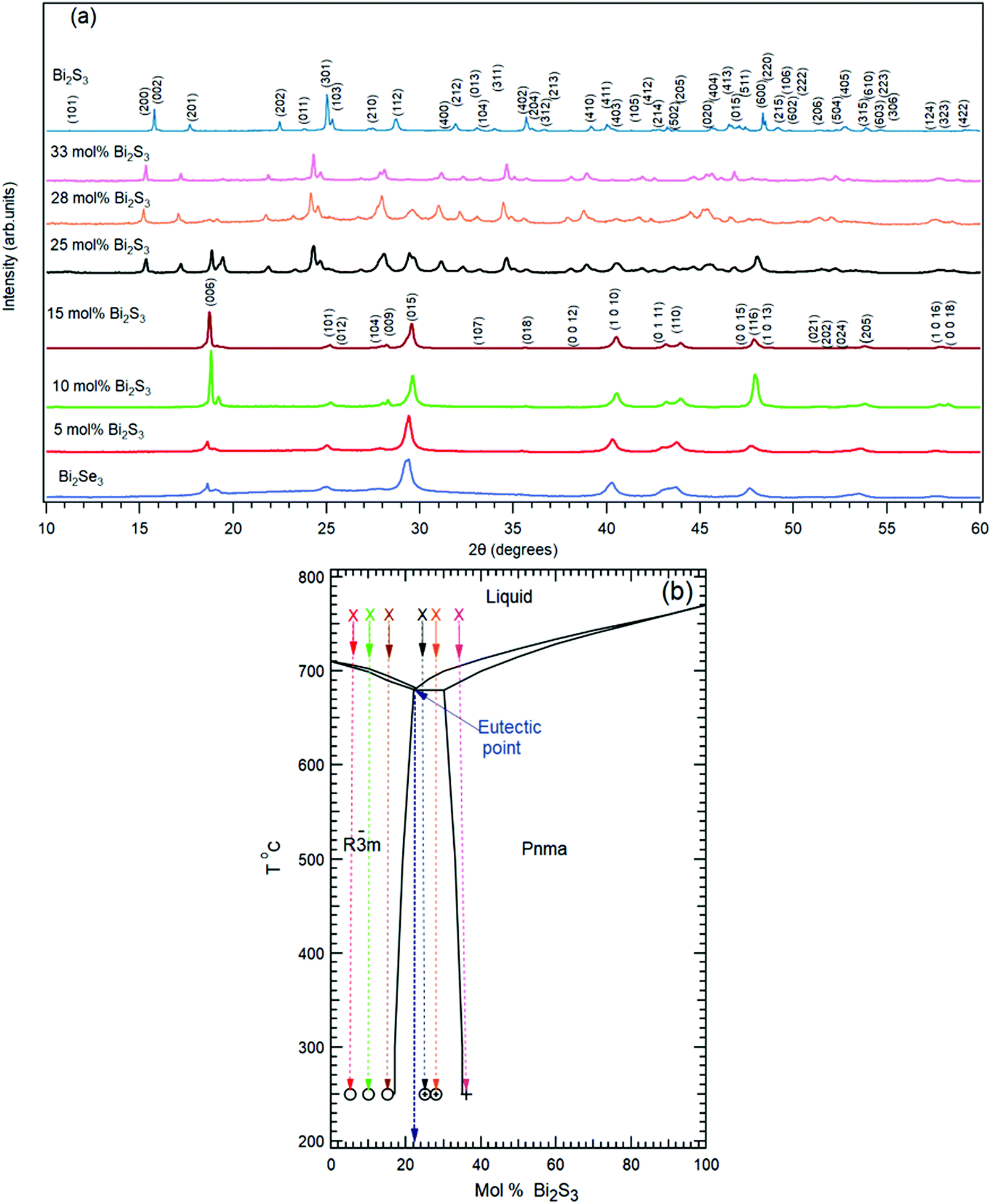 | ||
| Fig. 1 (a) Powder XRD patterns measured on the samples extracted from the ingots with different nominal mol% of Bi2S3 as indicated in (b). The measured patterns of pure Bi2Se3 and Bi2S3 corresponding to PDF #00-033-0214 and PDF #03-065-2431 respectively are reported. (b) Phase diagram of Bi2S3–Bi2Se3.14 Crosses represent the liquid phase, open circles the rhombohedral phase and plus signs the orthorhombic phase. | ||
 | ||
| Fig. 2 LEED pattern measured on (a) Bi2Se3 and (b) Bi2Se2.34S0.66 at primary electron energy of 66 eV. | ||
Recently, transport measurements on Bi2Se3−ySy with 0 ≤ y ≤ 0.21 indicated the existence of a TSS accompanied by unusual negative magnetoresistance behaviour.15 In a study of the SrxBi2Se3−ySy alloy (x = 0.066 and 0 ≤ y ≤ 0.4), it has been indirectly proved that sulphur destroys TSSs and suppresses superconductivity of SrxBi2Se3 as a result of a sulphur occupational disorder.16
Angle-resolved photoemission spectroscopy (ARPES) has been used to probe in a direct way the electronic structures of different ternary chalcogenides.17 The available ARPES results show that Bi2Se2S is not a topological insulator17 in contrast with the theoretical prediction.11,12 This result is interpreted as a consequence of the fact that the solid solution Bi2Se3−ySy prefers the rhombohedral structure at higher concentration of heavier Se, and the orthorhombic structure at higher concentration of lighter S.
Overall, a picture that reconciles the theoretical and experimental results on the topological properties of the Bi2Se3–Bi2S3 quasi-binary compounds is still lacking. We revisited the electronic properties of these systems along the entire compositional tie line with the use of bulk sensitive technique X-ray diffraction (XRD) and surface sensitive techniques low energy electron diffraction (LEED), scanning electron microscopy (SEM) with energy dispersive X-ray spectroscopy (EDX), X-ray photoemission spectroscopy (XPS) and ARPES. Spin-resolved ARPES was also employed to access the spin structure of the compounds. We show that rhombohedral single crystal structures are obtained only within the solid solution interval 0 – 22% mol of Bi2S3. All these systems possess spin polarized TSSs, in close analogy with the parent Bi2Se3 TI.
Experimental details
Bismuth and selenium were purchased from Sigma Aldrich. Sulphur was purchased from Acros Organics. Bi and S were 99.999% trace metal basis while Se was ≥99.5% trace metal basis. High quality single crystals along the Bi2Se3–Bi2S3 compositional tie line were grown by the Bridgman method. Stoichiometric amounts of high purity elements were sealed in evacuated quartz ampoules and heated up to 750 °C at 21 °C h−1. The ampoules were maintained at that temperature for 48 h. Thereupon the temperature was slowly reduced to 250 °C at 5 °C h−1 and then cooled down to room temperature.Seven different charges were prepared: pure Bi2Se3, 5 mol% Bi2S3, 10 mol% Bi2S3, 15 mol% Bi2S3, 25 mol% Bi2S3, 28 mol% Bi2S3, 33 mol% Bi2S3 and pure Bi2S3.
The XRD patterns of the powdered samples were collected with Rigaku Miniflex600 apparatus. The chemical composition was determined by fitting the EDX spectra measured with Oxford XMax-80 apparatus (with Aztech acquisition and analysis software) installed on a Jeol JSM-7100F field-emission SEM. Table 1 reports the nominal composition of the charges, composition estimated from the EDX analysis and corresponding y value in the chemical formula Bi2Se3−ySy of the samples studied by means of photoemission spectroscopy (see Fig. 3–6).
| Nominal composition of the charge (Bi2S3 mol%) | Measured composition from EDX spectra (Bi2S3 mol%) | Calculated y from EDX spectra |
|---|---|---|
| 5 | 3.8 ± 0.4 | 0.11 ± 0.01 |
| 10 | 10.8 ± 0.9 | 0.32 ± 0.03 |
| 15 | 14.3 ± 0.4 | 0.43 ± 0.01 |
| 25 | 22 ± 1 | 0.66 ± 0.03 |
| 33 | 36.7 ± 1.3 | 1.10 ± 0.04 |
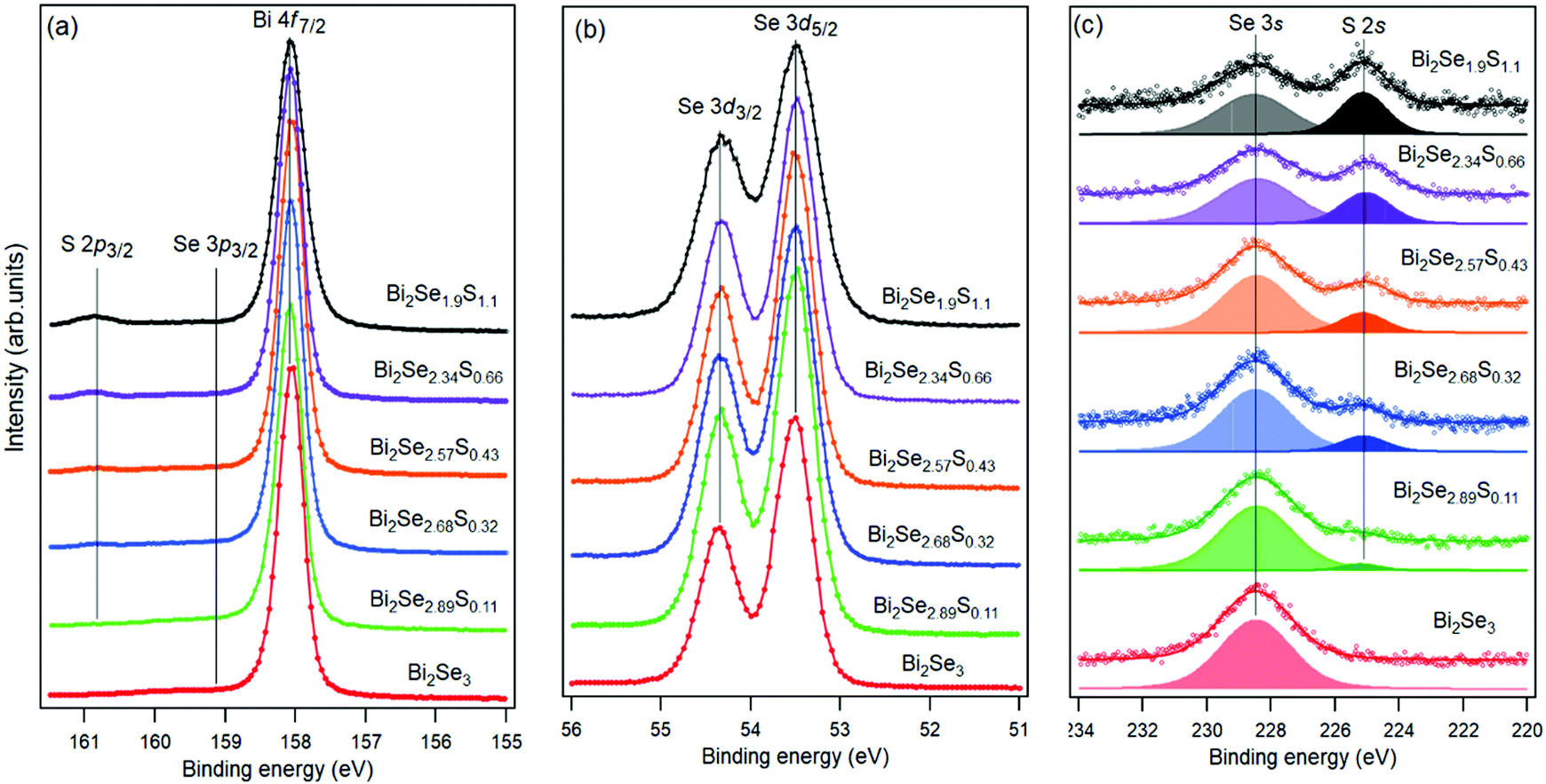 | ||
| Fig. 3 Bi 4f, Se 3d, Se 3s and S 2s core level spectra measured on the samples extracted from the charges with the composition indicated in the figures. Fitting curves are reported in the case of Se 3s and S 2s core levels. In the energy region of Bi 4f, the peaks corresponding to S 2p and Se 3p core levels are also visible with very low intensity. | ||
The photoemission experiments were carried out at Elettra synchrotron, Trieste, Italy on clean surfaces obtained by cleaving the samples in situ in ultra-high vacuum with pressure lower than 1.2 × 10⁻¹⁰ mbar. LEED was used to monitor the crystalline structure and quality of the surface. The XPS experiments were carried out at a VUV-Photoemission beamline using a Scienta R4000 hemispherical electron energy analyzer. All the XPS spectra were measured at room temperature using photon energy of 650 eV with a total energy resolution of ∼200 meV. S 2p and Se 3s core level spectra were fitted using Voigt functions. The ARPES measurements were carried out at the APE-LE beamline using a VG Scienta DA30 hemispherical electron energy analyzer. The spin-resolved ARPES measurements were performed with the Very Low Energy Electron Diffraction B (VLEED-B) polarimeter in the in-plane magnetization configuration (spin parallel to the sample surface in the direction perpendicular to the analyzer slit, i.e. perpendicular to the angular dispersion direction).18 The measurements were carried out in a 30° angular mode. The electron energy analyzer is mounted 45° with respect to the photon beam direction and the spectra collected near normal emission. ARPES and spin-resolved ARPES measurements were carried out with an overall energy resolution of 40 meV and 100 meV energy resolution respectively.
Results and discussion
The crystalline structure of the samples was analyzed by powder XRD (Fig. 1(a)).The samples corresponding to the pure Bi2Se3 composition and the nominal compositions with 5, 10 and 15 mol% of Bi2S3 were found to crystallize in the rhombohedral structure (Fig. 1(a)). EDX analysis of the single crystals extracted from the ingots showed that they possess a homogeneous chemical composition corresponding to the nominal composition of the charges. The XRD patterns of the samples with 25 and 28 mol% of Bi2S3 showed diffraction peaks corresponding to both the orthorhombic and rhombohedral structure. The coexistence of the two different phases is in accordance with the Bi2S3–Bi2Se3 phase diagram (Fig. 1(b))14 where the two-phase (orthorhombic and rhombohedral) range at room temperature extends from ∼16 to 33 mol% of Bi2S3. Interestingly, we could extract a 400 × 400 μm2 rhombohedral single crystal from the sample with nominal 25 mol% Bi2S3. Also, in this case the EDX analysis showed a homogeneous composition, with 22 ± 1 mol% of Bi2S3 and an S content exceeding the room-temperature solid solubility limit. This apparent anomaly can be explained with the phase diagram by Liu et al.14 and the crystal growth conditions. We grew our crystals by cooling from the liquidus field. During cooling of the 25% Bi2S3 sample the rhombohedral phase with the eutectic composition crystallized first. Because the line separating the rhombohedral phase field from the two-phase field is temperature-dependent and shifts to higher Bi2S3 content with increasing the temperature, the crystallized rhombohedral phase contains more sulphur. Obviously, such state is frozen during further cooling to room temperature and results in the supersaturated Bi2S3–Bi2Se3 solid solution. This allows us to investigate the rhombohedral solid solution in the extended range up to 22 mol% Bi2S3.
The chemical and electronic properties of the Bi2Se3−ySy alloys were analyzed with XPS and ARPES using synchrotron radiation. The spot sizes used for the XPS and ARPES analyses are of ∼200 × 50 μm2 and ∼150 × 50 μm2, respectively. Chemically homogeneous crystals, with areas larger than the spot sizes have been characterized ex situ by SEM-EDX before and after the photoemission experiments. From here on, samples are indicated by their chemical composition obtained by the EDX analysis (see Table 1) according to formula Bi2Se3−ySy. During the photoemission experiments, the crystalline structure of the sample surfaces was checked by means of LEED. For S content in the 0 < y ≤ 0.66 range we observed sharp spots forming a hexagonal diffraction pattern like that of Bi2Se3 (Fig. 2). This is indicative that our preparation gives rise to large and crystallographically ordered domains exposing the (0001) plane of the rhombohedral phase. According to the threefold symmetry of the Bi2Se3 (0001) surface (plane group p3m1) two sets of reflections with different intensity are expected in the LEED pattern,19 in contrast to our experimental pattern. A possible explanation for this behavior is that the electron energy of 66 eV minimizes the intensity contrast between the non-equivalent first order reflections. Alternatively, the presence of stacking faults in the crystal can produce 180° rotated domains,20 and then result in a hexagonal pattern. The latest scenario is more frequent in epitaxially grown films than in bulk crystals. The LEED pattern of the orthorhombic phase (not shown) has rectangular symmetry.
An insight into the chemical properties of the surface of different solid solutions was obtained by XPS (Fig. 5). The binding energy (BE) of Bi 4f7/2 (158.0 eV), Se 3d5/2 (53.3 eV), Se 3s (228.5 eV), and S 2s (225.0 eV) does not change as a function of S content and corresponds to that of Bi, Se and S atoms in Bi2Se321 and Bi2S3.22 This is an indication that S prevalently substitutes Se in Bi2Se3, and does not form clusters or an inhomogeneous distribution as proposed in ref. 15 to explain the anomalous transport properties of the Bi2Se3−ySy alloys.
Fig. 4 reports the electronic band structure measured near the Fermi level (EF). All Bi2Se3−ySy compounds with 0 ≤ y ≤ 0.66 possess two linearly dispersive bands crossing at Γ at 0.31 ± 0.045 eV BE. They have a surface character, as their dispersion does not change as a function of the photon energy (see Fig. 5).23,24 We identify these features as TSSs and their crossing as the Dirac point (DP). A DP below EF is an indication of electron doping caused by defects.24 The variation of the DPs within ± 45 meV can be due to slightly different concentration of intrinsic defects in the samples. These changes do not depend in a monotonic way on the S content and so are not assigned to S-driven doping effects. TSSs disappear at the composition Bi2Se2S, which is purely orthorhombic (magenta spectrum in Fig. 1(a)) and expected to exhibit the electronic properties of a trivial insulator.
 | ||
| Fig. 4 Electronic band structure measured near EF by means of ARPES on different Bi2Se3−ySy samples. Maps (a–e) were measured with hν = 50 eV, and map (f) with hν = 45 eV. k‖ = 0 Å−1 represents the Γ point. Dashed lines in panel (a,b,d and e) delimit stripes of the photoemission map of width Δk‖ = 0.048 Å−1 and centered at kn = −0.03 Å−1 and kp = +0.06 Å−1. EDCm↑↓ were collected within these stripes (in order to increase the signal to noise ratio) and used to extract the SEDCs reported in Fig. 6(a)–(h) (see text). | ||
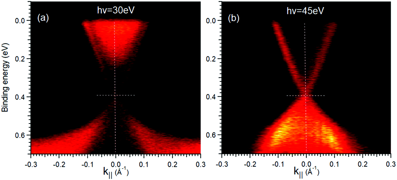 | ||
| Fig. 5 Electronic band structure of Bi2Se2.68S0.32 near EF measured with (a) hν = 30 eV and (b) hν = 45 eV. k‖ = 0 Å−1 represents the Γ point. The chosen photon energies do not change the dispersion of the TSS, but strongly modulate the intensity of the surface and bulk features. | ||
The systematic ARPES measurements clearly show that TSSs are not destroyed by diluting Bi2Se3 with Bi2S3 as long as the rhombohedral crystal symmetry is maintained. In the Bi2Se3−ySy this is possible up to y = 0.66. For higher S content, it is impossible to obtain a thermodynamically stable rhombohedral structure.
Fig. 6 reports the spin analysis of the electronic structure of the Bi2Se3−ySy samples. The spin-resolved measurements are carried out with the VLEED-B polarimeter in the in-plane magnetization configuration. In this configuration, the measured Energy Distribution Curves for the two opposite directions of the target magnetization m (EDCm↑↓) are used to calculate the in-plane spin polarization P using the formula  , where S = 0.3 is the effective Sherman function.18 The EDCm↑↓ were collected in the two Δk‖ intervals centered at kp and kn and of width 0.048 Å−1, which are indicated by dashed lines in Fig. 4. We point out that kp and kn are non-symmetric with respect to Γ. The spin-resolved electron distribution curves (SEDCs) extracted from the measured EDCm↑↓ using the formula
 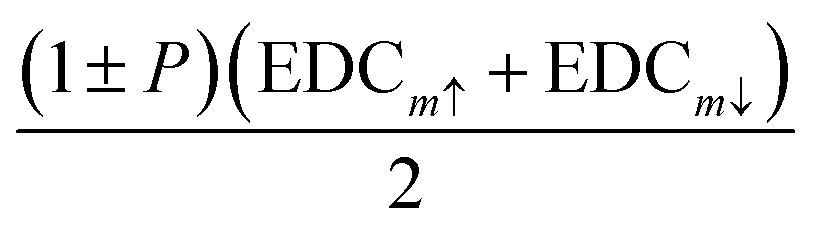 are reported in Fig. 6(a–h). The corresponding spin polarizations P are reported in Fig. 6(i–l).
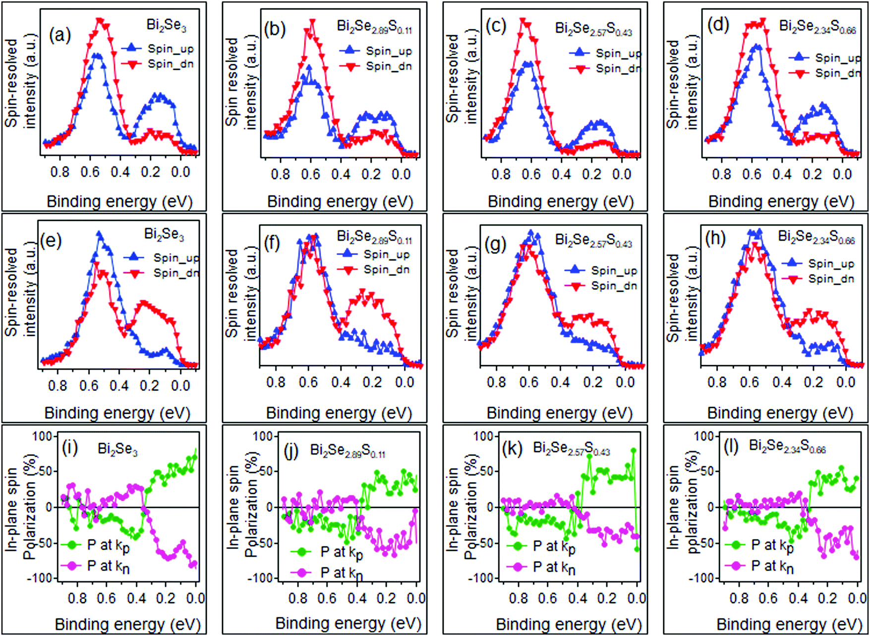 | ||
| Fig. 6 (a–d) Spin-resolved electron distribution curves extracted from the EDCm↑↓ measured at kp and (e–h) at kn on different Bi2Se3−ySy samples. The corresponding in-plane spin polarizations P at kp (green) and P at kn (magenta) are shown in (i–l). All the spectra were measured at photon energy 50 eV at T = 78 K. | ||
In all SEDCs there are two features: one between ∼0.3 eV BE and EF, and another one between ∼0.3 and ∼0.7 eV BE. The first feature is entirely ascribed to the upper branch of the TSS and displays the expected reversal of P at the opposite sides of Γ. The behaviour of the second feature is less clear due to the overlap of the lower branch of the TSS with the bulk valence states, which tends to reduce P, and the asymmetric acquisition geometry. For pure Bi2Se3, P is much lower at kn than at kp (Fig. 6(i)). This is even more clear for the S containing samples (Fig. 6(j–l)), where P approaches zero for kn but is finite for kp. However, these spurious effects do not hide the overall similar spin structure for the Bi2Se3−ySy samples with 0 ≤ y ≤ 0.66.
In summary, high quality single crystals of Bi2Se3−ySy could be prepared with the Bridgman method. The ARPES and spin-resolved ARPES measurements unambiguously show that the Bi2Se3−ySy solid solution supports a spin-polarized TSS for S content in the range 0 ≤ y ≤ 0.66. For these compositions, it is possible to isolate rhombohedral single crystals having homogeneous structural and chemical properties over an area of hundreds of μm.2 The core level spectra show that upon S incorporation, Bi is 3+, Se and S are 2− and no metallic species are formed. This is an indication that S most likely substitutes Se in Bi2Se3 and does not form clusters or an inhomogeneous distribution as proposed by ref. 15. With S incorporation the DP of Bi2Se3 does not shift systematically. As soon as the structure changes from rhombohedral to orthorhombic, the material becomes a trivial insulator.
Conflicts of interest
There are no conflicts to declare.Acknowledgements
The authors acknowledge the financial support from the Slovenian Research Agency (research core funding No. P2-0412), the project EUROFEL-ROADMAP ESFRI and Elettra, Trieste, Italy for the synchrotron facility. This work has been partly performed in the framework of the nanoscience foundry and fine analysis (NFFA-MIUR Italy Progetti Internazionali) facility.References
- C. L. Kane and E. J. Mele, Phys. Rev. Lett., 2005, 95, 226801 CrossRef CAS PubMed.
- A. R. Mellnik, J. S. Lee, A. Richardella, J. L. Grab, P. J. Mintun, M. H. Fischer, A. Vaezi, A. Manchon, E. A. Kim, N. Samarth and D. C. Ralph, Nature, 2014, 511, 449–451 CrossRef CAS PubMed.
- W. G. Vandenberghe and M. V. Fischetti, Nat. Commun., 2017, 8, 14184 CrossRef CAS PubMed.
- J. W. McIver, D. Hsieh, H. Steinberg, P. Jarillo-Herrero and N. Gedik, Nat. Nanotechnol., 2012, 7, 96–100 CrossRef CAS PubMed.
- P. Di Pietro, M. Ortolani, O. Limaj, A. Di Gaspare, V. Giliberti, F. Giorgianni, M. Brahlek, N. Bansal, N. Koirala, S. Oh, P. Calvani and S. Lupi, Nat. Nanotechnol., 2013, 8, 556–560 CrossRef CAS PubMed.
- J. Xiao, L. Kou, C. Y. Yam, T. Frauenheim and B. Yan, ACS Catal., 2015, 5, 7063–7067 CrossRef CAS.
- M. Neupane, S. Basak, N. Alidoust, S. Y. Xu, C. Liu, I. Belopolski, G. Bian, J. Xiong, H. Ji, S. Jia, S. K. Mo, M. Bissen, M. Severson, H. Lin, N. P. Ong, T. Durakiewicz, R. J. Cava, A. Bansil and M. Z. Hasan, Phys. Rev. B: Condens. Matter Mater. Phys., 2013, 88, 165129 CrossRef.
- Z. Ren, A. A. Taskin, S. Sasaki, K. Segawa and Y. Ando, Phys. Rev. B: Condens. Matter Mater. Phys., 2010, 82, 241306 CrossRef.
- L. Bao, L. He, N. Meyer, X. Kou, P. Zhang, Z. G. Chen, A. V. Fedorov, J. Zou, T. M. Riedemann, T. A. Lograsso, K. L. Wang, G. Tuttle and F. Xiu, Sci. Rep., 2012, 2, 726 CrossRef PubMed.
- H. Ji, J. M. Allred, M. K. Fuccillo, M. E. Charles, M. Neupane, L. A. Wray, M. Z. Hasan and R. J. Cava, Phys. Rev. B: Condens. Matter Mater. Phys., 2012, 85, 201103 CrossRef.
- H. Lin, T. Das, L. A. Wray, S. Y. Xu, M. Z. Hasan and A. Bansil, New J. Phys., 2011, 13, 095005 CrossRef.
- X. Ma, D. Chang, C. Zhao, R. Li, X. Huang, Z. Zeng, X. Huang and Y. Jia, J. Mater. Chem. C, 2018, 6, 13241–13249 RSC.
- M. Beglaryan and N. K. Abrikosov, Dokl. Akad. Nauk SSSR, 1959, 128, 345–347 CAS.
- H. Liu, C. R. Knowles and L. L. Y. Chang, Can. Mineral., 1995, 33, 115–128 CAS.
- R. Singh, V. K. Gangwar, D. D. Daga, A. Singh, A. K. Ghosh, M. Kumar, A. Lakhani, R. Singh and S. Chatterjee, Appl. Phys. Lett., 2018, 112, 102401 CrossRef.
- H. Huang, J. Gu, M. Tan, Q. Wang, P. Ji and X. Hu, Sci. Rep., 2017, 7, 45565 CrossRef CAS PubMed.
- M. Neupane, S. Y. Xu, L. A. Wray, A. Petersen, R. Shankar, N. Alidoust, C. Liu, A. Fedorov, H. Ji, J. M. Allred, Y. S. Hor, T. R. Chang, H. T. Jeng, H. Lin, A. Bansil, R. J. Cava and M. Z. Hasan, Phys. Rev. B: Condens. Matter Mater. Phys., 2012, 85, 235406 CrossRef.
- C. Bigi, P. K. Das, D. Benedetti, F. Salvador, D. Krizmancic, R. Sergo, A. Martin, G. Panaccione, G. Rossi, J. Fujii and I. Vobornik, J. Synchrotron Radiat., 2017, 24, 750–756 CrossRef CAS PubMed.
- X. Guo, Z. J. Xu, H. C. Liu, B. Zhao, X. Q. Dai, H. T. He, J. N. Wang, H. J. Liu, W. K. Ho and M. H. Xie, Appl. Phys. Lett., 2013, 102, 151604 CrossRef.
- S. Roy, H. L. Meyerheim, K. Mohseni, A. Ernst, M. M. Otrokov, M. G. Vergniory, G. Mussler, J. Kampmeier, D. Grützmacher, C. Tusche, J. Schneider, E. V. Chulkov and J. Kirschner, Phys. Rev. B: Condens. Matter Mater. Phys., 2014, 90, 155456 CrossRef.
- V. V. Atuchin, V. A. Golyashov, K. A. Kokh, I. V. Korolkov, A. S. Kozhukhov, V. N. Kruchinin, S. V. Makarenko, L. D. Pokrovsky, I. P. Prosvirin, O. K. N. Romanyuk and O. E. Tereshchenko, Growth, 2011, 3, 5507–5514 CrossRef.
- J. Grigas, E. Talik and V. Lazauskas, Phys. Status Solidi, 2002, 230, 220–230 CrossRef.
- J. Sánchez-Barriga, I. Aguilera, L. V. Yashina, D. Y. Tsukanova, F. Freyse, A. N. Chaika, C. Callaert, A. M. Abakumov, J. Hadermann, A. Varykhalov, E. D. L. Rienks, G. Bihlmayer, S. Blügel and O. Rader, Phys. Rev. B, 2018, 98, 235110 CrossRef.
- Z. H. Pan, E. Vescovo, A. V. Fedorov, D. Gardner, Y. S. Lee, S. Chu, G. D. Gu and T. Valla, Phys. Rev. Lett., 2011, 106, 257004 CrossRef PubMed.
| This journal is © The Royal Society of Chemistry 2021 |