
 Open Access Article
 This Open Access Article is licensed under a
 Creative Commons Attribution 3.0 Unported Licence
Inverted organic photovoltaics with a solution-processed ZnO/MgO electron transport bilayer†
Ioannis
Ierides
 a,
Isaac
Squires
a,
Giulia
Lucarelli
b,
Thomas M.
Brown
b and
Franco
Cacialli
*a
a,
Isaac
Squires
a,
Giulia
Lucarelli
b,
Thomas M.
Brown
b and
Franco
Cacialli
*a
aDepartment of Physics and Astronomy and London Centre for Nanotechnology, University College London, London, WC1H 0AH, UK. E-mail: f.cacialli@ucl.ac.uk; Tel: +44 (0)20 7679 4467
bCHOSE (Centre for Hybrid and Organic Solar Energy), Department of Electronic Engineering, University of Rome Tor Vergata, Italy
First published on 16th February 2021
Abstract
Electron transport layers (ETLs) have been instrumental in breaking the efficiency boundaries of solution-processed photovoltaics. In particular, bilayer ETLs with an MgO top component have afforded tremendous success in various solution-processed systems, such as perovskite photovoltaics, however, their application in the promising technology of organic photovoltaics is limited. In this work, we fabricate organic photovoltaic devices incorporating a “bilayer” ZnO/MgO ETL instead of a single ZnO ETL, so as to reduce the leakage current and boost the power conversion efficiency. The ZnO/MgO ETL is shown to have a more uniform top surface and a lower work function compared to the single ZnO ETL which is expected to be beneficial to electron extraction. Furthermore, we demonstrate that insertion of the thin (≲ 10 nm) MgO interlayer in devices leads to a reduced leakage current and an increase in the shunt resistance. Application of the MgO interlayer boosts the short circuit current density and fill factor, and enhances the power conversion efficiency by ∼10% (relative increase) thereby demonstrating a facile approach to push the efficiency of organic photovoltaics to higher levels.
1 Introduction
Solution-processed photovoltaic systems benefit from the advantage of cheap fabrication over large areas and provide windows of opportunity for novel photovoltaic applications.1,2 Hence intense research efforts have been focused on both organic and inorganic solution-processed systems, ranging from quantum dots,3 polymers4,5 and small molecules6 to perovskite photovoltaics.7–9A common strategy employed to increase efficiency in the vast majority of these systems is the implementation of a multilayer stack, where the active layer is sandwiched between an electron transport layer (ETL) and a hole transport layer (HTL) prior to the addition of electrodes on either side. These layers can serve different functions in each of the aforementioned systems. They can be used to modify the interfacial energetics of the device10 by matching and controlling the work function of different components and thus increase the built-in field,11 and/or form ohmic contacts,12 to name but a few examples. Ultimately, their common purpose in all cases is to facilitate charge transport and extraction.
In the case of inverted organic photovoltaics (OPVs), a plethora of materials have been investigated for application as ETLs. For a comprehensive review we direct the reader to the review by Yin et al.12 A key example is the polymer poly[(9,9-bis(3′-(N,N-dimethylamino)propyl)-2,7-fluorene)-alt-2,7-(9,9-dioctylfluorene)] known as PFN13 that is used to reduce the work function of ITO. There are of course many other examples.14,15 Interestingly, the prevailing ETLs in inverted OPVs are semiconducting metal oxides since they have the combined ability to effectively extract/transport electrons due to their relatively high mobilities and at the same time offer good solution-processability, high optical transparency and good environmental stability.12 The most widely employed metal oxide is ZnO. Indeed, ZnO has been the “elective” ETL for the latest state-of-the-art inverted OPV devices16,17 affording higher efficiency than other metal oxides such as TiO2.
However, solution-processed ZnO is a sub-optimal ETL. For example, it can suffer from surface defects that can act as electron trap sites and result in severe charge recombination losses.18,19 The application of a thin or ultrathin interlayer between ZnO and the active layer to form a bilayer ETL has proven to be a simple and effective method to improve ZnO-based inverted OPVs through various mechanisms (incidentally, some of these interlayers, also because of their reduced thickness, lack morphological uniformity, to the point of calling into question the appropriateness of the “bilayer” diction – for convenience, and following the practice of previous literature, we will still refer in some places to the combined ZnO/MgO ETL as a “bilayer” even though some evidence is presented that our MgO films also lack uniformity, so that a more accurate description might be that of an “interlayer” for the ZnO/MgO combination).
For example, Abd-Ellah et al.20 employed a carboxylic acid as the modifying interlayer that decreased the work function of the ETL by ∼0.4 eV, and boosted both the short-circuit current density (Jsc) and fill factor (FF) with respect to devices based on a single ZnO ETL. Similarly, Wang et al.18 formed a ZnO/In ETL nanojunction with indium films (≤1 nm thick) that reduced recombination by filling the traps, and decreased the contact barrier potential thereby facilitating carrier transport and extraction. In addition, formation of In2O3 provided an efficient energy cascade from the fullerene component of the active layer to ZnO. An increase in Jsc and the FF has also been achieved by the passivation of traps on the surface of ZnO through the formation of bilayer ETLs with MoS2 quantum dots,19 poly(vinylpyrrolidone) and polyethylene glycol,21 calcium fluoride22 and solid alcohol 1-pyrenemethanol23 serving as the modifying interlayers. Other interlayers such as a pyrene BODIPY molecular dye24 and commercially available dispersants D181 and D18725 applied between ZnO and the active layer, optimised the active layer morphology. Recently, it has been demonstrated that biomaterials such as DNA26 and processed spinach leaves27 can serve as effective modifying interlayers in bilayer ZnO ETLs. In all the above cases the use of a bilayer ETL led to enhanced power conversion efficiencies (PCEs) when compared with a single ZnO ETL. The recent resurgence of OPVs2 has led to device efficiencies exceeding 18%28 in state-of-the-art single junctions. The application of a bilayer ETL rather than a single ETL may enable further efficiency improvements. This motivated us to search for other materials that can be applied successfully as modifying interlayers.
Recent studies of other solution-processed photovoltaic systems with a bilayer ETL based on MgO captured our attention. Dagar and collaborators29 for example demonstrated SnO2/MgO bilayer ETLs in CH3NH3PbI3 perovskite cells reaching efficiencies up to 19% under 1 sun. This represented an increase of ∼20% compared to the single SnO2 ETL that was attributed to an improved ETL film quality as the presence of MgO removed pinholes on the SnO2 surface, and to a reduced interfacial carrier recombination. Similarly, Han et al.30 employed a TiO2/MgO bilayer ETL improving the efficiency by ∼10% compared to the single TiO2 ETL. Besides CH3NH3PbI3 perovskites the use of a bilayer ETL incorporating MgO as a top component (and thus in contact with the active layer) has also been demonstrated in other solution-processed systems. Jayaweera et al.31 used an SnO2/MgO ETL effectively to form CdS nanosheet sensitized photovoltaics. This study was preceded by the study of Docampo et al.,32 where an SnO2/MgO bilayer ETL was applied to both solid state and electrolyte dye sensitised solar cells leading to a tripling and almost doubling of the efficiency for the two cases respectively, compared to their single SnO2 ETL counterparts. By employing transient photovoltage and charge collection measurements it was demonstrated that the presence of MgO favorably shifts the conduction band edge of the ETL by 200 mV, thereby partly enabling the increase in open circuit voltage (Voc), hence increasing performance. It is important to note that the mechanism by which the bilayer MgO based ETL facilitated the performance enhancement with respect to having a single ETL, differs in each of the above instances and necessitates a separate investigation in each case to uncover it. MgO has a very high ionisation potential (∼10 eV – see Fig. 1a) and an insulating nature. These characteristics may serve to decrease the current leakage in OPV devices. The question therefore arises as to whether MgO could be applied effectively as a modifying interlayer in OPVs so as to increase their performance.
 | ||
| Fig. 1 (a) Approximate energy levels for the different components used in the OPV device (values have been obtained from the literature18,29,36,39,40). In the case of MoO3 we report a relatively large range (please note the rectangle is not meant to indicate the energy gap but the spread of reported values of work function) since it is known that the work function depends strongly on the preparation conditions. We had also measured values ∼5.1 eV in our own laboratory). The thicknesses of the layers are approximately 30 nm (ZnO), 10/150 nm (MgO), 100 nm (active layer), 10 nm (MoO3) and 80 nm (Au). (b) Schematic of the multi-layered structure of the OPV device. (c) Representative current density–voltage curves under 1 sun. Here the current density for the device with the thicker MgO layer (150 nm) has been multiplied by a factor of 10 to aid legibility. The thickness of the MgO layer is ∼10 and 150 nm when the precursor is spin-coated at 5000 and 3000 rpm respectively. Note the very slight but clearly visible change in Voc (∼5 mV) for the selected devices. (d) Representative current density–voltage curves in the dark. | ||
In this work, we investigate MgO as a modifying interlayer on top of a ZnO ETL formed by simple solution-processing and low temperature annealing and apply it to OPVs (see Fig. 1b for the OPV device structure). We show that the modified ETL enhances the performance of OPV devices with respect to the single ZnO ETL. The use of an MgO interlayer for OPVs has not been reported previously, with the exception of a very recent publication33 that uses a different device architecture (namely with the MgO not in direct contact with the active layer but “buried” below the ZnO film), and of which we became aware of in the final stages of the preparation of this manuscript. Both studies show that the application of MgO in ETLs for OPVs can lead to enhanced performance, thus demonstrating the excellent potential of MgO. In the study by Huang et al.33 FTO/MgO/ZnO is used for electron extraction. In our study, the electron extractor system is ITO/ZnO/MgO and MgO is used as the top component of the system. To investigate the origin of the performance enhancement resulting from the addition of MgO in our device structure, in addition to the typical current density–voltage and external quantum efficiency (EQE) characterisation of our devices, we present atomic force microscopy (AFM), Kelvin probe measurements and optical spectroscopy (namely transmittance, absorbance and electroabsorption). These measurements enable us to demonstrate that insertion of the thin (≲ 10 nm) MgO interlayer in OPV devices leads to reduced leakage current and an increase in the shunt resistance by a factor of 2 compared to devices with only a single ZnO ETL. Furthermore, we show that the ZnO/MgO ETL has a more uniform top surface with a root mean square (rms) roughness decreasing from 4.5 ± 0.2 nm to 3.2 ± 0.4 nm and a lower work function by 0.11 ± 0.05 eV. We discuss the origin of the (slightly) lower work function that seems to be associated with the electrostatic compression effect of MgO34 on metal oxides.
2 Experimental
2.1 Device fabrication
![[thin space (1/6-em)]](https://www.rsc.org/images/entities/char_2009.gif) :1.5. The solution was then allowed to stir overnight at room temperature. All the above processes were carried out in a glovebox under a nitrogen environment. The PTB7-Th:ITIC-2F solution was formed by dissolving 10 mg of PTB7-Th in 1 mL chlorobenzene and 15 mg of ITIC-2F in 0.25 mL of chlorobenzene. The individual solutions were stirred for 4 hours and then mixed together along with 26 μL of 1,8-diiodooctane to yield a 20 mg mL−1 concentration with blend ratio of 1:1.5. The solution was then allowed to stir overnight at room temperature. The above processes were carried out in a glovebox under a nitrogen environment as well. The F8BT solution was formed by dissolving 10 mg of F8BT in 1 mL of toluene. The solution was then allowed to stir overnight at room temperature in the nitrogen glovebox. The ZnO solution was formed by dissolving 0.1 g zinc acetate dihydrate and 28 μL ethanolamine in 1 mL of 2-methoxyethanol. The solution was then stirred vigorously for 12 hours at room temperature. The SnO2 solution was formed by dissolving 45.13 mg of tin chloride dihydrate in 2 mL ethanol and stirring overnight at room temperature. The MgO solution was formed by dissolving 5 mg of magnesium acetate tetrahydrate in 1 mL of ethanol and stirring overnight at room temperature.
:1.5. The solution was then allowed to stir overnight at room temperature. All the above processes were carried out in a glovebox under a nitrogen environment. The PTB7-Th:ITIC-2F solution was formed by dissolving 10 mg of PTB7-Th in 1 mL chlorobenzene and 15 mg of ITIC-2F in 0.25 mL of chlorobenzene. The individual solutions were stirred for 4 hours and then mixed together along with 26 μL of 1,8-diiodooctane to yield a 20 mg mL−1 concentration with blend ratio of 1:1.5. The solution was then allowed to stir overnight at room temperature. The above processes were carried out in a glovebox under a nitrogen environment as well. The F8BT solution was formed by dissolving 10 mg of F8BT in 1 mL of toluene. The solution was then allowed to stir overnight at room temperature in the nitrogen glovebox. The ZnO solution was formed by dissolving 0.1 g zinc acetate dihydrate and 28 μL ethanolamine in 1 mL of 2-methoxyethanol. The solution was then stirred vigorously for 12 hours at room temperature. The SnO2 solution was formed by dissolving 45.13 mg of tin chloride dihydrate in 2 mL ethanol and stirring overnight at room temperature. The MgO solution was formed by dissolving 5 mg of magnesium acetate tetrahydrate in 1 mL of ethanol and stirring overnight at room temperature.
For the transmittance/absorbance, AFM and Kelvin probe investigations we prepared samples with varying structures. All layers in these samples were processed with the same conditions used for the corresponding layers in OPVs.
Lastly, samples intended for the testing of the ITO and ITO/SnO2 substrates via electroabsorption spectroscopy were fabricated in the same manner as OPVs, but instead of a blend, F8BT was employed as the active layer that was deposited via spin-coating at 1000 rpm for 90 seconds in the nitrogen glovebox. These samples were not encapsulated and their measurement was carried out under vacuum (∼10−3 mbar).
2.2 Device characterisation
In electroabsorption spectroscopy we probe the manifestation of non-linear optical effects that cause a variation in the absorption spectrum of the system of interest due to the application of a modulating electric field. More specifically we measure the normalised variation of light transmitted through a sample upon application of a periodic electric field. The schematic of the home-built apparatus used to perform the measurement is shown in Fig. S2 (ESI†). More details regarding the apparatus and method by which the built-in voltage is extracted can be found in previous work.35,36 In brief, the response of our system can be modelled using the framework of Stark effect theory.37 This leads to the equation  where
where  is the electroabsorption signal, G(hν) describes the spectral dependence, VDC is the applied DC voltage, VBI is the built-in voltage and VAC is the applied AC voltage. As evident from the equation, application of a DC voltage equal to the built-in voltage will cause the signal to vanish. Hence the built-in voltage of a device can be extracted at the point where the applied DC voltage nulls the signal. The above analysis assumes that there are no interfering spectral contributions (e.g. from permanent dipole moments possibly associated to polar molecules). To confirm this, we plot electroabsorption spectra with different applied DC and AC voltages and show that the isosbestic points always intersect at the point where the electroabsorption signal is nulled, hence there are no interfering contributions (that would cause the isosbestic point to shift) confirming the validity of using the stated method.38
3 Results and discussion
3.1 ZnO/MgO based inverted organic photovoltaics
The current density–voltage characteristics at 1 sun for OPVs based on a single ZnO ETL vs. the bilayer ZnO/MgO ETL (where MgO was deposited at 5000 rpm or 3000 rpm) are shown in Fig. 1c. The corresponding average key photovoltaic performance indicators are set out in Table 1. The active materials used in the blend are PTB7-Th and PC70BM. The application of the ZnO/MgO bilayer rather than the single ZnO layer (when MgO is kept sufficiently thin ∼10 nm) successfully enhances the performance, boosting the PCE by ∼10%. This is achieved mainly through an increase in Jsc and in the FF. The increase in Jsc has also been verified by the calculation of the photocurrent from EQE spectra (Fig. S3 and Table S1, ESI†) which is in agreement with the extracted data from the current density–voltage investigations. It is important to note that the efficient operation of OPVs employing the MgO interlayer requires the layer to be kept ultrathin. For the case of the thicker MgO devices (spin-coated at 3000 rpm with resulting thickness of ∼150 nm) a poor performance is obtained with an efficiency of 0.03 ± 0.02%. This is a result of a very low Jsc of 0.2 ± 0.1 mA cm−2 and FF of 0.26 ± 0.02. The origin of the aforementioned changes in performance is investigated and discussed in detail in Section 3.2.| Sample | PCE (%) | J sc (mA cm−2) | V oc (V) | FF |
|---|---|---|---|---|
| ITO/ZnO/PTB7-Th:PC70BM/MoO3/Au | 3.98 ± 0.16 | 10.6 ± 0.5 | 0.72 ± 0.01 | 0.53 ± 0.03 |
| ITO/ZnO/MgO(5000 rpm)/PTB7-Th:PC70BM/MoO3/Au | 4.31 ± 0.14 | 10.9 ± 0.2 | 0.72 ± 0.01 | 0.55 ± 0.02 |
| ITO/ZnO/MgO(3000 rpm)/PTB7-Th:PC70BM/MoO3/Au | 0.03 ± 0.02 | 0.2 ± 0.1 | 0.73 ± 0.01 | 0.26 ± 0.02 |
To demonstrate that the application of an MgO bilayer ETL can be extended to more types of OPVs, we have applied this strategy to other systems as well and assessed its effectiveness. The representative current density–voltage characteristic curves and the corresponding average key photovoltaic performance indicators for all the modifications can be found in Fig. S4 and Table S2 (ESI†). Where not otherwise specified the MgO precursor was spin-coated at 5000 rpm. Firstly, we substituted the Au top contact with Ag (that can serve as a cheaper alternative) and also tested devices without the MoO3 HTL. Although the PCE of these devices is lower than the devices presented in Fig. 1, in all cases, the use of the bilayer MgO ETL instead of the single ETL boosted the performance through an increase in the Jsc and FF. We also tested OPVs with an SnO2 ETL, however these devices yielded an “s-shaped” current density–voltage characteristic curve. Such an “s-shaped” curve for SnO2 only ETLs in OPV devices have been previously reported in the literature, e.g. by Tran et al.41 The physical mechanism responsible for this behaviour has been attributed to accumulation of charge carriers within the device.42 Tran et al. mitigated the occurrence of “s-shaped” characteristics by incorporating a bilayer SnO2/CsCO3 ETL in the device structure. Similarly, our SnO2/MgO bilayer removes some of the “s-shape” behavior. Finally, devices with a blend containing the non-fullerene acceptor ITIC-2F rather than PC70BM as the acceptor have also been tested. The substitution of the single ZnO ETL to the ZnO/MgO ETL for these devices led to an efficiency boost of ∼15% in relative terms, further demonstrating the wider applicability of MgO based bilayer ETLs in OPVs.
3.2 The effects of MgO as a top component in bilayer electron transport layers
While the effectiveness and reproducibility of the ZnO/MgO ETL for OPVs is demonstrated in Section 3.1, it is essential to understand the effects of introducing the ultrathin MgO modifying film in the OPV devices. In general, an increase in performance similar to the one we witnessed in the previous section is likely to be associated with one (or more) of the following mechanisms:18(1) An improved rate of photon capture which depends strongly on the transmittance of the semi-transparent cell electrode.
(2) A favorable change in the active layer blend morphology leading to higher exciton dissociation.
(3) Reduced leakage current leading to a higher shunt resistance.
(4) A change in the interfacial energetics of the interface between the ETL and blend by a variation of the ETL's work function.
In the rest of this section we present evidence to help establish the extent to which the above mechanisms occur due to the presence of MgO and identify the origin of the success of MgO as an interlayer for OPVs.
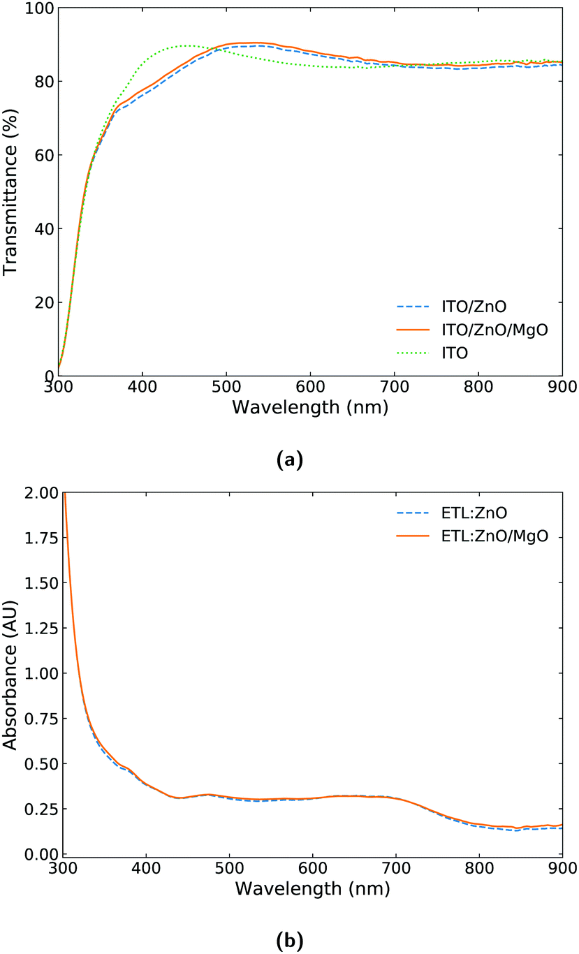 | ||
| Fig. 2 (a) Transmittance of ITO, ITO/ZnO, ITO/ZnO/MgO(5000 rpm) films. (b) Absorbance spectra of thin films comparing the ITO/ZnO/PTB7-Th:PC70BM with the ITO/ZnO/MgO(5000 rpm)/PTB7-Th:PC70BM structures. The addition of MgO seems to have a negligible effect. | ||
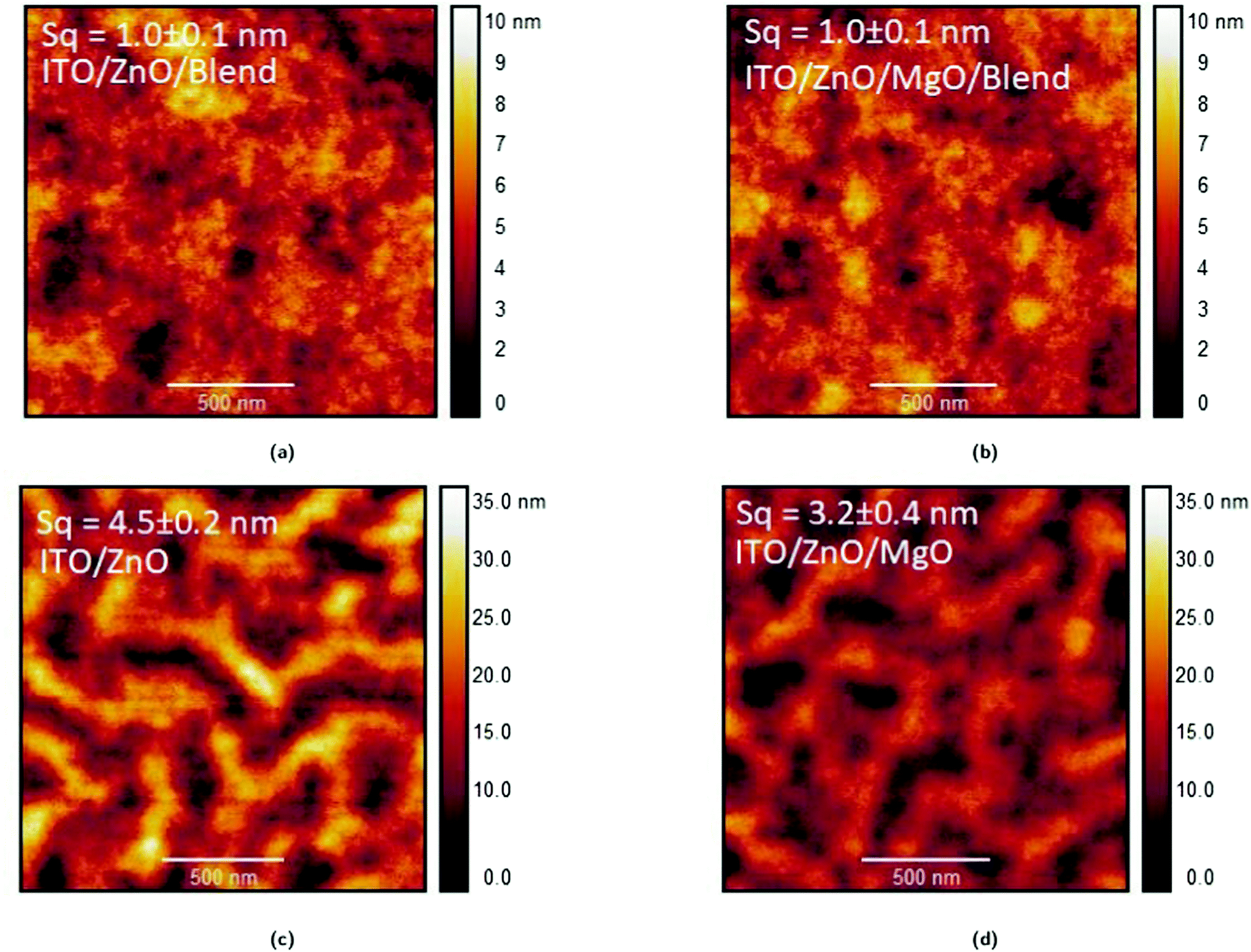 | ||
| Fig. 3 Tapping mode AFM images of the topography of (a) ITO/ZnO/PTB7-Th:PC70BM, (b) ITO/ZnO/MgO(5000 rpm)/PTB7-Th:PC70BM where surface morphology is almost indistinguishable and (c) ITO/ZnO, (d) ITO/ZnO/MgO(5000 rpm) where a variation in root mean square (rms) roughness is observed. | ||
| Sample | Active layer | ΔW (eV) | ΔVBI (V) |
|---|---|---|---|
| ITO/(MgO) | F8BT | −0.50 ± 0.05 | 0.46 ± 0.03 |
| ITO/ZnO/(MgO) | Blend | −0.11 ± 0.05 | 0.05 ± 0.03 |
| ITO/SnO2/(MgO) | F8BT | −0.20 ± 0.05 | 0.19 ± 0.03 |
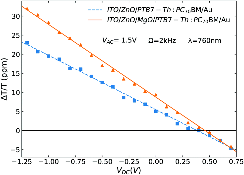 | ||
| Fig. 4 Electroabsorption signal vs. DC voltage plots used to extract the built-in voltage in the single ETL and bilayer ETL OPV devices. The parameters used for the experiments are displayed in the Figure. The MgO layer thickness is ∼10 nm for the relevant device. | ||
3.3 Origin of the work function modification by the addition of MgO
The application of MgO and work function modification on different metals and semiconductors has been extensively studied in the literature as a promising solution for catalysis.49 Three main mechanisms that have been identified to dictate work function modifications in general are the electrostatic compressive effect, charge transfer and surface relaxation. For the case of MgO, the electrostatic compressive effect can give a significant contribution.34 This effect enables the MgO layer to form a surface dipole on the metal or semiconductor surface even in the absence of charge transfer. The different levels of the contribution of these mechanisms can give considerable differences in the final change in work function, hence the change in work function can be rather different for different substrate materials. This explains why such different values of work function shift (ΔW) are observed upon MgO application for the different substrates used in our investigations (as shown in Table 2). In Fig. 5 we present further Kelvin probe measurements of the dependence of work function shift (ΔW) on the thickness of MgO deposited on top of the substrate. The thicknesses are approximately 10, 150 and 350 nm as measured by profilometry corresponding to 5000, 3000 and 1000 rpm spin coating deposition speeds. The reduction of work function seems to be thickness independent for ITO and ITO/SnO2, whilst for ITO/ZnO, it seems to be thickness dependent only at very small thicknesses (which may be a result of partial coverage). This overall thickness independence points towards an interfacial mechanism being responsible for the decrease in work function and hence our findings further support and are in line with the established findings in the literature.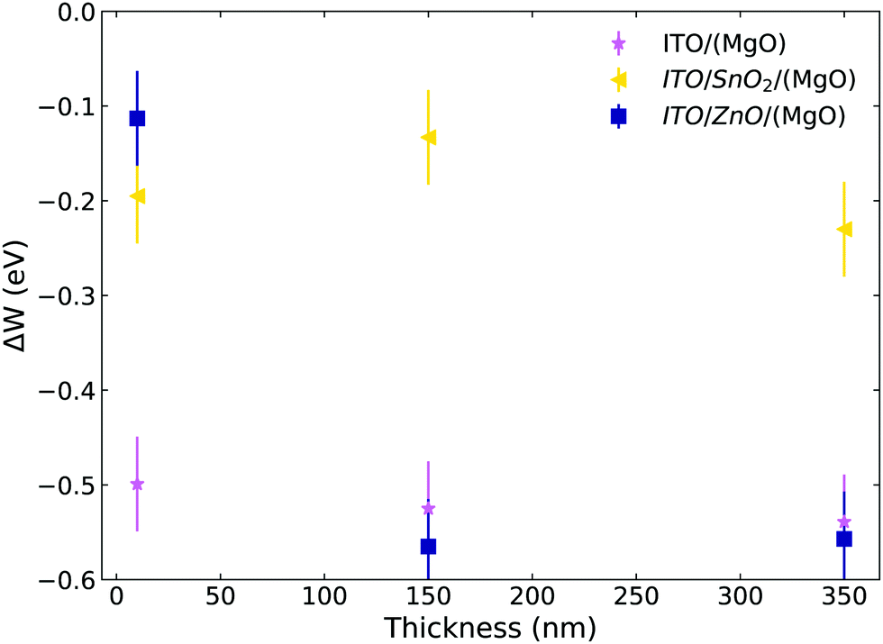 | ||
| Fig. 5 Kelvin probe measurements showing the change in the work function of different substrates upon addition of the MgO layer with varying thickness. | ||
4 Conclusions
In this work, we have investigated the application of low cost, non-toxic ultrathin (∼10 nm) MgO as a potential modifying interlayer to serve as the top component of bilayer ETLs applied to OPVs. The use of the ZnO/MgO bilayer rather than single ZnO as ETL, led to a ∼10% and ∼15% increase in efficiency in relative terms for devices consisting of a blend with a fullerene acceptor and a non-fullerene acceptor respectively. The increase in PCE was a result of an enhanced Jsc and FF, which we can trace down to a reduction in the leakage current and an increase in the shunt resistance of devices. The presence of MgO leads to a number of favourable characteristics. Without significantly affecting the photon capture rate and blend morphology, the MgO interlayer offers an improved contact as demonstrated by the reduction of the surface roughness of the ETL and the lower work function. This leads to a better energy level matching with the LUMO of the photovoltaic blend acceptor that results in enhanced charge extraction. The lower work function is shown to originate from an interfacial interaction between the MgO and the metal oxide that is consistent with the so-called electrostatic compressive effect. Through our investigations, we show that high transparency and a high ionisation potential can serve as useful design rules for future ETLs but more importantly our study serves as proof that inspiration for future ETLs for OPVs can be drawn by novelties in other solution-processed systems and that transfer of developments from one field to another can be a viable route to synergistically push the performance boundaries of these promising technologies to even higher levels.Conflicts of interest
There are no conflicts to declare.Acknowledgements
Special thanks to Natalie Stingelin, Alessandro Minotto and Andrea Zampetti for useful discussions. We acknowledge use of the London Centre for Nanotechnology Atomic Force Microscope Facility. II was supported by the EPSRC and SFI Centre for Doctoral Training in Advanced Characterisation of Materials (grant number EP/L015277/1). TMB received support from MIUR through the PRIN2017 BOOSTER project (no. 2017YXX8AZ). FC thanks EPSRC for financial support via grant EPSRC: EP/P007767/1.Notes and references
- M. Graetzel, R. A. J. Janssen, D. B. Mitzi and E. H. Sargent, Nature, 2012, 488, 304–312 CrossRef CAS
.
- I. Ierides, A. Zampetti and F. Cacialli, Curr. Opin. Green Sustainable Chem., 2019, 17, 15–20 CrossRef
- M. Y. M. Liu and E. H. Sargent, Nat. Energy, 2016, 1, 16016 CrossRef
- K. A. Mazzio and C. K. Luscombe, Chem. Soc. Rev., 2015, 44, 78–90 RSC
- C. Yan, S. Barlow, Z. Wang, H. Yan, A. K.-Y. Jen, S. R. Marder and X. Zhan, Nat. Rev. Mater., 2018, 3, 18003 CrossRef CAS
- S. D. Collins, N. A. Ran, M. C. Heiber and T.-Q. Nguyen, Adv. Energy Mater., 2017, 7, 1602242 CrossRef
- Q. Lin, A. Armin, P. L. Burn and P. Meredith, Acc. Chem. Res., 2016, 49, 545–553 CrossRef CAS
- P. Papagiorgis, A. Manoli, S. Michael, C. Bernasconi, M. I. Bodnarchuk, M. V. Kovalenko, A. Othonos and G. Itskos, ACS Nano, 2019, 13, 5799–5809 CrossRef CAS
- J. Dagar, S. Castro-Hermosa, G. Lucarelli, A. Zampetti, F. Cacialli and T. M. Brown, IEEE J. Photovolt., 2019, 9, 1309–1315 Search PubMed
- R. J. E. Westbrook, D. I. Sanchez-Molina, D. J. Manuel Marin-Beloqui, D. H. Bronstein and D. S. A. Haque, J. Phys. Chem. C, 2018, 122, 1326–1332 CrossRef CAS
- J.-H. Lee, S. Y. Jeong, G. Kim, B. Park, J. Kim, S. Kee, B. Kim and K. Lee, Adv. Funct. Mater., 2018, 28, 1705079 CrossRef
- Z. Yin, J. Wei and Q. Zheng, Adv. Sci., 2016, 3, 1500362 CrossRef
- Z. He, C. Zhong, S. Su, M. Xu, H. Wu and Y. Cao, Nat. Photonics, 2012, 6, 591–595 CrossRef
- H.-L. Yip and A. K.-Y. Jen, Energy Environ. Sci., 2012, 5, 5994–6011 RSC
- P. Li, Z. Jiang, H. Huang, S. Tian, X. Hu, W. Li, X. Bao and Y. Wang, Mater. Sci. Semicond. Process., 2020, 116, 105150 CrossRef CAS
- Y. Lin, Y. Firdaus, M. I. Nugraha, F. Liu, S. Karuthedath, A.-H. Emwas, W. Zhang, A. Seitkhan, M. Neophytou, H. Faber, E. Yengel, I. McCulloch, L. Tsetseris, F. Laquai and T. D. Anthopoulos, Adv. Sci., 2020, 7, 1903419 CrossRef CAS
- X. Du, Y. Yuan, L. Zhou, H. Lin, C. Zheng, J. Luo, Z. Chen, S. Tao and L.-S. Liao, Adv. Funct. Mater., 2020, 30, 1909837 CrossRef CAS
- C. Wang, D. Luo, Y. Gao, G. Wang, C. Wang, P. Ma, H. Li, S. Wen, W. Dong and S. Ruan, J. Phys. Chem. C, 2019, 123, 16546–16555 CrossRef CAS
- J. Xie, X. Wang, S. Wang, Z. Ling, H. Lian, N. Liu, Y. Liao, X. Yang, W. Qu, Y. Peng, W. Lan and B. Wei, Org. Electron., 2019, 75, 105381 CrossRef CAS
- M. Abd-Ellah, J. Cann, S. V. Dayneko, A. Laventure, E. Cieplechowicz and G. C. Welch, ACS Appl. Electron. Mater., 2019, 1, 1590–1596 CrossRef CAS
- X. Zhang, Y. Sun, M. Wang, H. Cui, W. Xie, L. Shen and W. Guo, Sol. Energy, 2019, 181, 9–16 CrossRef CAS
- Y. Tang, Y. Pang, X. Li, B. Zong, B. Kang, S. R. P. Silva and G. Lu, J. Colloid Interface Sci., 2020, 562, 142–148 CrossRef CAS
- X. Cai, T. Yuan, X. Liu and G. Tu, ACS Appl. Mater. Interfaces, 2017, 9, 36082–36089 CrossRef CAS
- A. Soultati, A. Verykios, S. Panagiotakis, K.-K. Armadorou, M. I. Haider, A. Kaltzoglou, C. Drivas, A. Fakharuddin, X. Bao, C. Yang, A. R. B. M. Yusoff, E. K. Evangelou, I. Petsalakis, S. Kennou, P. Falaras, K. Yannakopoulou, G. Pistolis, P. Argitis and M. Vasilopoulou, ACS Appl. Mater. Interfaces, 2020, 12, 21961–21973 CrossRef CAS
- Y.-Y. Yu, C. Tseng, W.-C. Chien and C.-P. Chen, Org. Electron., 2019, 69, 20–25 CrossRef CAS
- J. Dagar, G. Scavia, M. Scarselli, S. Destri, M. De Crescenzi and T. M. Brown, Nanoscale, 2017, 9, 19031–19038 RSC
- Q. Rong, Q. Zhang, M. Cui, L. Nian, D. Zheng, X. Gao, L. Shui, G. Zhou and N. Li, Org. Electron., 2020, 81, 105669 CrossRef CAS
- Q. Liu, Y. Jiang, K. Jin, J. Qin, J. Xu, W. Li, J. Xiong, J. Liu, Z. Xiao, K. Sun, S. Yang, X. Zhang and L. Ding, Sci. Bull., 2020, 65, 272–275 CrossRef CAS
- J. Dagar, S. Castro-Hermosa, G. Lucarelli, F. Cacialli and T. M. Brown, Nano Energy, 2018, 49, 290–299 CrossRef CAS
- G. S. Han, H. S. Chung, B. J. Kim, D. H. Kim, J. W. Lee, B. S. Swain, K. Mahmood, J. S. Yoo, N.-G. Park, J. H. Lee and H. S. Jung, J. Mater. Chem. A, 2015, 3, 9160–9164 RSC
- E. N. Jayaweera, G. R. Kumara, C. Kumarage, S. K. Ranasinghe, R. M. G. Rajapakse, H. M. N. Bandara, O. A. Ileperuma and B. S. Dassanayake, J. Photochem. Photobiol., A, 2018, 364, 109–115 CrossRef CAS
- P. Docampo, P. Tiwana, N. Sakai, H. Miura, L. Herz, T. Murakami and H. J. Snaith, J. Phys. Chem. C, 2012, 116, 22840–22846 CrossRef CAS
- S. Huang, B. Kang, L. Duan and D. Zhang, J. Colloid Interface Sci., 2021, 583, 178–187 CrossRef CAS
- S. Prada, U. Martinez and G. Pacchioni, Phys. Rev. B, 2008, 78, 235423 CrossRef
- T. M. Brown, J. S. Kim, R. H. Friend, F. Cacialli, R. Daik and W. J. Feast, Appl. Phys. Lett., 1999, 75, 1679–1681 CrossRef CAS
- T. M. Brown, G. M. Lazzerini, L. J. Parrott, V. Bodrozic, L. Bürgi and F. Cacialli, Org. Electron., 2011, 12, 623–633 CrossRef CAS
- I. H. Campbell, T. W. Hagler, D. L. Smith and J. P. Ferraris, Phys. Rev. Lett., 1996, 76, 1900–1903 CrossRef CAS
- E. Siebert-Henze, V. G. Lyssenko, J. Fischer, M. Tietze, R. Brueckner, M. Schwarze, K. Vandewal, D. Ray, M. Riede and K. Leo, AIP Adv., 2014, 4, 047134 CrossRef
- Ossila, PC70BM, https://www.ossila.com/products/pc70bm.
- Ossila, PTB7-Th, PCE-10, https://www.ossila.com/products/pce10.
- V.-H. Tran, S. H. Eom, S. C. Yoon, S.-K. Kim and S.-H. Lee, Org. Electron., 2019, 68, 85–95 CrossRef CAS
- B. Qi and J. Wang, Phys. Chem. Chem. Phys., 2013, 15, 8972–8982 RSC
- F. Zhao, L. Deng, K. Wang, C. Han, Z. Liu, H. Yu, J. Li and B. Hu, ACS Appl. Mater. Interfaces, 2020, 12, 5120–5127 CrossRef CAS
- A. Savva, F. Petraki, P. Elefteriou, L. Sygellou, M. Voigt, M. Giannouli, S. Kennou, J. Nelson, D. D. C. Bradley, C. J. Brabec and S. A. Choulis, Adv. Energy Mater., 2013, 3, 391–398 CrossRef CAS
- M. Neukom, S. Züfle, S. Jenatsch and B. Ruhstaller, Sci. Technol. Adv. Mater., 2018, 19, 291–316 CrossRef CAS
- M. Wang, Y. Sun, J. Guo, Z. Li, C. Liu and W. Guo, Org. Electron., 2019, 74, 258–264 CrossRef CAS
- G. D. M. R. Dabera, J. Lee and R. A. Hatton, Adv. Funct. Mater., 2019, 29, 1904749 CrossRef CAS
- S. Huang, N. Ali, Z. Huai, J. Ren, Y. Sun, X. Zhao, G. Fu, W. Kong and S. Yang, Org. Electron., 2020, 78, 105555 CrossRef CAS
- T. Jaouen, G. Jézéquel, G. Delhaye, B. Lépine, P. Turban and P. Schieffer, Appl. Phys. Lett., 2012, 100, 022103 CrossRef
Footnote |
| † Electronic supplementary information (ESI) available. See DOI: 10.1039/d0tc04955g |
| This journal is © The Royal Society of Chemistry 2021 |